SANTTU KOSKINEN
ANALYSIS OF INKJET-PRINTED FLEX-MODULE IN A
MO-BILE PHONE
Master of Science Thesis
The subject was approved by the Faculty Council of Computing and Electrical Engineering
June 8th 2011
Examiners: Prof. Jukka Vanhala, Dr. Matti Mäntysalo
II
ABSTRACT
TAMPERE UNIVERSITY OF TECHNOLOGY
Master's Degree Programme in Electrical Engineering
SANTTU KOSKINEN: Analysis of Inkjet-printed Flex-module in a Mobile Phone
Master of Science Thesis, 63 pages, 14 Appendix pages October 2011
Major: Electronics
Examiners: Prof. Jukka Vanhala, Dr. Matti Mäntysalo
Keywords: exible electronics, inkjet, printable electronics, electronics manufacturing technology, laser processing
Flexible circuit boards are becoming more and more common in small and lightweight consumer electronics devices. Manufacturers are seeking novel technologies for ex-ible circuit manufacturing. Cost-eciency, environmental eects of the manufactur-ing technology and reducmanufactur-ing process steps in manufacturmanufactur-ing are the key drivers for development. Printed electronics, especially inkjet technology, has been an emerg-ing viable candidate for exible circuit board manufacturemerg-ing over the last few years. Additive processing, minimal material consumption and digitally guided processing are the main attractors of inkjet printing technology.
The objective of this thesis work is to demonstrate a exible circuit board of a commercial mobile phone with inkjet printing technology. The design of the exi-ble printed circuit board is transferred to inkjet printing technology. The assembly process of the ex module is presented, including laser processing of the substrate, inkjet printing of the circuit layout, component attachment using isotropically con-ductive adhesive and epoxy and circuit coating. The end result is a exible circuit, similar to the original design, produced with a new manufacturing technology. The inkjet printed demonstrators were then electrically tested by the original manufac-turer of the device. Testing showed that functional prototypes with close to the same performance of the original devices were manufactured.
The target of the thesis work was reached. Functional demonstrators with good performance were manufactured with inkjet printing technology. As other outcome knowledge of manufacturing electronics with inkjet printing was further increased, as methods for the design and assembly phase were developed. A specic image masking algorithm for processing of the inkjet printer bitmap images was introduced in the device design phase. Method for making vias on substrate with inkjet printing technology was demonstrated. Also a method for component attachment on exible inkjet printed circuits was demonstrated.
III
TIIVISTELMÄ
TAMPEREEN TEKNILLINEN YLIOPISTO Sähkötekniikan koulutusohjelma
SANTTU KOSKINEN: Matkapuhelimessa käytettävän inkjet-tulostetun tai-puisan piirilevyn analyysi
Diplomityö, 63 sivua, 14 liitesivua Lokakuu 2011
Pääaine: Elektroniikka
Tarkastajat: Prof. Jukka Vanhala, Matti Mäntysalo, TkT
Avainsanat: taipuisa elektroniikka, inkjet, painettava elektroniikka, elektroniikan valmis-tustekniikka, laserprosessointi
Kuluttajaelektroniikkalaitteiden koon pienentyessä taipuisat piirilevyt tulevat jatku-vasti yleisimmiksi laitteiden rakenteissa. Valmistajat pyrkivät kehittämään pii-rilevyn valmistusprosesseja jatkuvasti. Ajureina toimivat mm. valmistuksen ja materiaalien hinta, ympäristönäkökulmat, sekä valmistuksessa käytettävien proses-sivaiheiden määrän vähentäminen. Painettavan elektroniikan eri osa-alueet, erityi-sesti inkjet-teknologia, ovat pyrkineet viime vuosina tarjoamaan vaihtoehdon per-inteisille taipuisien piirilevyjen valmistusprosesseille. Inkjet teknologian houkuttele-vina puolina nähdään prosessin additiivisuus, vähäinen materiaalinkulutus, sekä di-gitaalisesti ohjattu valmistusprosessi.
Tämän opinnäytetyön tavoitteena on osoittaa inkjet-teknologian soveltuvuus tai-puisien piirilevyjen valmistukseen demonstraattorilaitteen kautta. Matkapuhelimes-sa käytettettävän taipuiMatkapuhelimes-san piirlevyn sunnittelutiedostoja muokkaamalla piirilevyn valmistustiedostot siirrettiin inkjet-teknologialla toteutettaviksi. Työssä käydään läpi valmistusprosessin eri vaiheet, kuten piirilevyn ulkoreunojen ja läpivientien laserleikkaus, johdotuskerrosten inkjet-painaminen, komponenttien liittäminen iso-trooppisesti johtavalla liimalla ja epoksilla, sekä piirilevyn päällystäminen suojaus-lakalla. Lopputuloksena on alkuperäisen kaltainen, uudella valmistusteknologialla valmistettu taipuisa piirilevy. Valmistetut prototyypit testattiin alkuperäisen valmis-tajan toimesta. Testausvaiheen päätelmänä voidaan todeta, että toimivia taipuisia piirilevy valmistettiin inkjet-teknologiaa hyväksikäyttäen ja valmistetut piirilevyt vastasivat sähköiseltä suorituskyvyltään suurilta osin alkuperäistä tuotetta.
Työlle asetettu tavoite saavutettiin. Toimivia taipuisia piirilevyjä valmistet-tiin inkjet-teknologiaa hyväksikäyttäen. Asetetun tavoitteen lisäksi työstä saavalmistet-tiin irti myös muuta hyödyllistä tietoa inkjet-teknologian käytöstä elektroniikan valmis-tuksessa. Sekä suunnittelu-, että valmistusvaiheessa käytettiin uusia menetelmiä. Kuvanmaskausalgoritmi mahdollisti tarkkojen rakenteiden tulostamisen. Piirilevyn läpiviennit valmistettiin käyttäen hyväksi laserleikkausta ja inkjet-teknologiaa, sekä työssä esitettiin eräs menetelmä komponenttien liittämiseen taipuisaan piirilevyyn.
IV
PREFACE
This M.Sc. work was done at the Department of Electronics at Tampere University of Technology. The thesis work was carried out as a part of PIPA project which is a collaborative project funded by Meadville, Nokia, Premix, Tekes (Finnish Funding Agency for Technology and Innovation), Tampere University of Technology, Univer-sity of Oulu and UPM.
I would like to thank the thesis work examiners Professor Jukka Vanhala and Doctor Matti Mäntysalo for guidance during the thesis work. In addition, I would like to thank Lasse Pykäri, Ying-Maria Dong and all other related personnel of Nokia for the help and support during this work.
I would also like to thank my present and former colleagues in the TUT Printable Electronics Group for ideas, fruitful conversations and support during the thesis work.
Lastly, I would like to thank my family and my friends for the support during this thesis work.
Tampere, Finland
V
TABLE OF CONTENTS
1. Introduction . . . 1
2. Flexible Electronics . . . 3
2.1 Flexible Circuits . . . 3
2.2 Common Flexible Circuit Manufacturing Processes . . . 4
2.2.1 Copper Processing Options . . . 5
2.2.2 Flexible Circuit Types . . . 5
2.2.3 Double-sided Flex Circuit Manufacture . . . 7
2.3 Flexible Printed Electronics and Inkjet Technology . . . 9
2.3.1 Inkjet Printer Operational Principles . . . 9
2.3.2 Inks in Inkjet Technology . . . 11
2.3.3 Nanoparticle Inks . . . 12
2.3.4 Nanoparticle Ink Jettability . . . 12
2.3.5 Nanoparticle Ink Wetting . . . 13
2.3.6 Sintering . . . 14
3. Device Design Conversion to Inkjet Technology . . . 17
3.1 Device Description . . . 17
3.1.1 Display and LEDs . . . 18
3.1.2 Keyboard . . . 20
3.1.3 Earpiece . . . 21
3.2 Material Selection . . . 22
3.3 PCB Layout from Gerber to Bitmap . . . 24
3.3.1 Changes to Original PCB Layout . . . 24
3.3.2 Background for Bitmap Masking Algorithm . . . 27
3.3.3 Bitmap Masking Algorithm . . . 29
4. Printed Flexmodule Assembly . . . 32
4.1 Kapton Polyimide Preheating . . . 32
4.2 Laser Processed Vias and Module Outline . . . 34
4.3 Inkjetted Circuit Board . . . 36
4.4 Component Attachment . . . 38
4.5 Conformal Coating . . . 39
4.6 Stiener Plates Laser Processing . . . 40
4.7 Mounting the Flexible PCB in the Mobile Phone and Initial Testing . 41 5. Analysis and Performance Testing . . . 42
5.1 Structural Comparison . . . 42
5.1.1 Layer thicknesses . . . 42
5.1.2 Via Structures . . . 44
VI 5.2 Performance Tests . . . 46 5.2.1 EMC Test . . . 47 5.2.2 ESD Test . . . 48 5.2.3 Antenna Test . . . 50 5.2.4 Display Test . . . 51 5.2.5 Audio Test . . . 52
5.2.6 Summary of Test Results . . . 56
6. Further Development . . . 57 7. Conclusions . . . 58 References . . . 60 A.Appendix . . . 64 B.Appendix . . . 72 C.Appendix . . . 76
VII
LIST OF NOTATION AND ABBREVIATIONS
dBm Dierence in decibels to one milliwatt
dBr Dierence in decibels to a specied reference level
dBµV/m Dierence in decibels to one microvolt per meter
DOD Drop on demand
DPI Dots per inch
DUT Device Under Test
EIRP Eective Isotropic Radiated Power
EMC Electromagnetic compatibility
ESD Electrostatic discharge
FPC Flexible printed circuit
HF High Frequency
Gerber A le format used in PCB manufacturing industry
ICA Isotropically conductive adhesive
LCD Liquid Crystal Display
LED Light Emitting Diode
PCB Printed circuit board
RE Radiated Emissions
RF Radio Frequency
RSE Radiated Spurious Emissions
RX Receive
SMT Surface Mount Technology
SPR Standard Product Requirements
TA Type Approval
TDMA Time Division Multiple Access
TIS Total Isotropic Sensitivity
TIFF Tagged image le format
TRP Total Radiated Power
1
1. INTRODUCTION
Consumer electronics devices tend to become ever smaller and lighter. One way of reducing the size and weight of an electronics device is to use exible circuit boards in devices, such as mobile phones, cameras and laptop computers. Usually the reason for using a exible circuit in the device body is a need for reduction in device size and weight, a need for placing the circuit on a non-at surface or a movable property needed in the device structure. Flexible circuits can be used to wrap a circuit around a device body in a stationary application, or to provide a hinge or a joint between moving parts in a dynamic application.
The drivers for seeking new manufacturing technologies to produce exible cir-cuits are many. Cost-ecient materials, environmental values and fewer process steps in manufacturing are preferred. Inkjet printing is an emerging technology which can be used for making exible electronics. The variety of materials which can be deposited using inkjet technology is constantly expanding. Conductive ma-terials [1], dielectrics [2] [3] and organic semiconductors [4] have been printed using inkjet technology. Manufacturing printed circuit boards by inkjet technology diers from the common manufacturing methods in some ways. Because inkjet technology is an additive process, the material waste in the manufacturing stage is minimal. All deposited material is used for the creation of the circuit as no material is taken away. In large scale manufacturing, this could have a positive environmental impact. Digital control of the printing process [5] enables easy and fast modications to cir-cuit board layout les, which is benecial for e.g. prototyping and small volume manufacturing purposes.
The objective of this thesis work is to demonstrate the applicability of inkjet printing for manufacturing of exible circuits through a demonstrator case. Circuit design of a exible circuit board of a mobile phone was taken and transferred for inkjet printing technology. A set of prototypes were manufactured by inkjet printing and their functionality was veried by electrical tests. This thesis covers the design modication, assembly and testing phases of a demonstrator manufactured by inkjet technology.
In chapter two traditional exible circuit manufacturing technologies are briey discussed and compared with inkjet printing. The focus is on the manufacturing on a two-sided exible circuit because of the demonstrator device. The idea is to
1. Introduction 2 give the reader sucient background to understand the characteristics of common manufacturing methods and inkjet printing technology.
In chapter three the demonstrator case is introduced. The material selection and the steps of transferring the design les to inkjet printing technology are gone through. Modications to the design les are discussed and a masking algorithm for improving printed image quality is presented.
In chapter four the assembly phase of the demonstrator prototypes is gone through. Substrate preparations, laser processing of the module outline and vias, inkjet print-ing of the circuit board, component attachment and circuit coatprint-ing methods are discussed in detail.
Chapter ve covers the testing phase and analysis of the test results. Details of the manufactured prototypes are compared with the original ex module with the help of cross-sectional images. Test procedures and results of electromagnetic compatibility (EMC) test, electrostatic discharge (ESD) test, antenna test, display test and audio test are discussed. Chapter six describes the future development that is to be carried out with the demonstrator case, but is not to be included in this thesis work. In chapter seven nal conclusions of the entire project are drawn.
3
2. FLEXIBLE ELECTRONICS
The term exible electronics is very wide and its meaning is constantly expanding due to progress and new innovations made in the industrial and research elds. Today the term covers areas such as exible displays, exible solar cells, exible sensors, exible thin-lm transistor circuits and exible circuits among other areas [6]. In this chapter the focus is on the characteristics and manufacturing of exible circuits. Making exible circuits by conventional means and by inkjet-printing are discussed.
2.1 Flexible Circuits
The history of exible circuits dates back to the turn of the 20th century. Patents issued at that time show that researchers were developing ways to make exible interconnections for example in telephony and military applications. During World War II exible circuits were adopted to military applications such as the German made V2 rocket [7]. Later on exible circuits have become essential part of every day electronic devices such as desktop printers, cameras, computers and mobile phones. Today exible circuit industry is a vast global market with countries like Japan and USA holding the most signicant market shares. [7]
The IPC-T-50 industry standard "Terms and Denitions for Printed Boards." de-nes exible circuit as "A patterned arrangement of printed wiring utilizing exible base material with or without exible cover layers". The denition is broad as is the variety of exible circuit types. The applications for exible circuits are many but these applications can be roughly divided into static and dynamic applications. In a static application the exibility of the circuit is needed when installing the circuit in the application but no actual exibility is needed during the use of the device. One example of a static exible circuit application can be seen in gure 2.1 where a exible circuit is wrapped around a camera body.
2. Flexible Electronics 4
Figure 2.1: A exible circuit in an Olympus Stylus camera. [8]
In a dynamic application the circuit is exed during use. Flexibility can be utilized in circuits that go through hinges like those in laptops and foldable mobile phones. Many desktop printers also have exible circuits which are used to connect moving parts. Dynamic applications especially place demands on the durability and reliability of interconnections and component joints in exible circuits. [7]
Aside from exibility, exible printed circuits (FPC) have also other attractive qualities compared with rigid printed circuit boards. FPCs oer reduction in package size as the used substrates are usually much thinner than rigid substrates. Reducing package size also leads to reduction in package weight.
2.2 Common Flexible Circuit Manufacturing Processes
The manufacturing processes in the exible circuit industry are many. Dierent pro-cess steps are used for producing single-sided, double-sided and multilayer circuits. In this section dierent processing options are discussed and the focus is on double-sided ex circuit manufacturing process. The idea is to give the reader a basis of a traditional manufacturing process to be compared later with a novel technology.
The basic elements of a exible circuit are polymer lm as the base material, possible bonding adhesive, metal foil and cover layer. A exible base material and metal are joined to create a laminate, on which the circuit is the processed. Usually polyimide or polyester is used as the base material. Bonding adhesive is used to attach the metal layer to the base material. It is also possible to manufacture adhesiveless metal clad laminates by either casting the polymer direct on to a carrier foil or by depositing a seed layer of copper on a base lm and building up the metal
2. Flexible Electronics 5 layer by electroplating. While copper is mostly used, other metals can be used to satisfy special demands. A cover layer is used to protect the conductors of a exible circuit. Cover layers can be e.g. laminated, photoimageable or screen-printed and cured by heat or UV-radiation.
2.2.1 Copper Processing Options
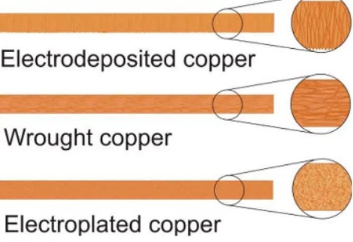
Due to copper's cost, good electrical performance and physical properties it is the most commonly used metal in exible circuit metallic layers. Copper can be de-posited on substrate by using various methods. Some of these methods and the grain orientations are presented in gure 2.2.
Electrodeposited copper is good for use in static applications, but due to the columnar grain structure it is not well suited for dynamic applications [7]. Wrought or rolled and annealed copper is produced by thinning copper with a series of metal rollers and then heat treating the metal foil. Commonly copper foils down to 18 µm thickness can be produced economically. Rolled and annealed copper is the most commonly used foil type in exible circuit applications and due to the grain structure it is well suitable for dynamic applications [7]. Electroplated copper is de-posited on a substrate by using a combination of electroless and electrolytic plating. Electroplated foils can be produced to have an amorphous grain structure.
Figure 2.2: Dierent copper lm production methods and grain structures. [7]
2.2.2 Flexible Circuit Types
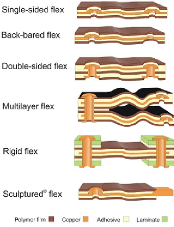
There are several constructions of exible circuits for several dierent applications. Depending on the complexity of the circuit design the exible circuit can be manufac-tured to have one, two or several conductive layers by using dierent manufacturing processes. Most common types of ex circuits are shown in gure 2.3.
2. Flexible Electronics 6
2. Flexible Electronics 7 The single-sided ex circuit is the simplest construction. A single-sided ex circuit consists of a conductor layer on a exible base lm and usually has a protective coating. Component connections can be made from one side only. A back-bared exible circuit is a similar to the single-sided ex circuit, but the conductive layer is accessible from both sides, thus enabling component connections on both sides.
Double-sided ex circuits have two conductive layers on a exible substrate. Usu-ally double-sided ex circuits have plated through vias for connecting the conductive layers and component connections can be made on either side. Double-sided ex circuits can be manufactured with a protective layer on one, both or neither side.
Multilayer ex circuits have three or more conductive layers. Usually the con-ductive layers are connected by plated through vias. The layers of a multilayer ex circuit can be separately laminated in some regions of the circuit to enable routings to dierent areas or to enable maximum exibility.
A rigid-ex circuit is a hybrid construction of a exible and a rigid substrate that are connected together into a single structure. The electrical interconnections in the rigid and exible interface are usually made by plated through vias. Rigid-ex circuits are usually multilayer constructions, but double-layer constructions also exist.
Sculptured ex circuits have conductors which vary in thickness in dierent places of the circuit. The usual goal is to make thin conductors in exible places and thick conductors at interconnection locations. Selective etching of copper foil is used to attain dierent thicknesses of conductors in dierent areas of the circuit. [7]
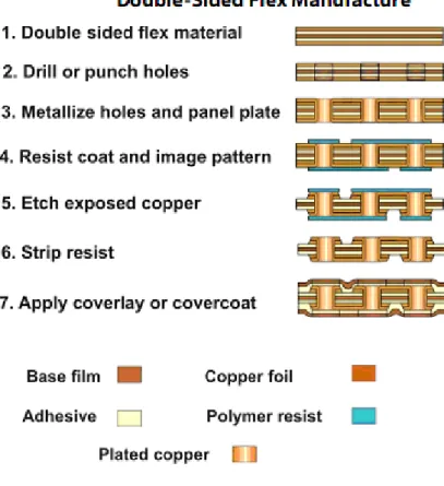
2.2.3 Double-sided Flex Circuit Manufacture
A typical panel plating manufacturing process for double-sided exible circuits is described in gure 2.4. The process starts with drilling or punching holes on a sub-strate. The substrate is plated with copper on either side. After the hole processing the holes are metalized using an electroless plating process or an alternative metal-lization process. After electroless metalmetal-lization the copper layer in the holes is built up to sucient thickness by electroplating.
After the plating of holes and the panel a resist image of the circuit pattern is applied on the both sides of the laminate. The exposed copper is then chemically etched and the remaining copper areas form the actual circuit. After etching the copper the remaining resist material needs to be stripped before applying the cover layer on top and bottom sides of the circuit board.
2. Flexible Electronics 8
2. Flexible Electronics 9
2.3 Flexible Printed Electronics and Inkjet Technology
Many traditional printing methods are making their way to electronics manufactur-ing. For example, gravure printing, exography and screen printing can be used for spreading conductive pastes, semiconductors and dielectrics on dierent sub-strates. Inkjet technology is one of the novel techniques being evaluated for the use of electronics manufacturing. Inkjet technology diers from the previously men-tioned printing methods in some ways. The pattern le is stored in a digital format, rather than in a physical format on a plate or a roll. Digital pattern format enables easy and fast pattern redesign and also lowers the xed costs in the beginning of the design process as there is no need for physical devices as gravure plates or ex-ographic printing plates. This is very benecial in small volume manufacturing and prototyping. Inkjet technology is also a contactless technology. This means that the deposition tool, the print head, does not touch the substrate during deposition pro-cess. Patterning on rigid and exible substrates is possible. Contactless deposition also enables processing on three dimensional substrates.
Manufacturing ex circuits by using inkjet-technology diers from common ex circuit manufacturing in several ways. Inkjet-printing is an additive process, where no excess material is deposited on the substrate while circuit processing. No pre-manufactured laminate of exible polymer lm and metal foil is needed before circuit processing as the circuit is inkjetted straight onto a polymer substrate. This way the material loss during circuit manufacturing is minimal. As conductors and dielectric layers can be processed without applying photoresist layers and etching chemicals, process steps are reduced and environmental load of the manufacturing process is small.
In this section the basic principles of producing electronic circuits using inkjet technology are presented. Emphasis is on making conductive circuits using inkjet technology, while other areas are may be covered with less attention. Inkjet printer operational principles are discussed along with nanoparticle ink properties.
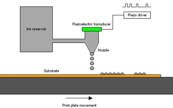
2.3.1 Inkjet Printer Operational Principles
Inkjet printer deposition methods can be divided into continuous deposition and Drop-on-Demand deposition. Continuous deposition means that drops are deposited in a steady rate, needed or not, and are then deected towards the substrate or collected to be used again. Drop-on-Demand means that a drop is red from the nozzle plate only when it is intended to be deposited on a substrate. Simplied diagram of the operation of a piezo-controlled Drop-on-Demand inkjet is presented in gure 2.5. Ink is fed from the ink reservoir to the nozzles and a drop is formed by actuating the ink inside the nozzle cavity by a pulse. The actuating pulse can be
2. Flexible Electronics 10 generated in several ways. Thermal, acoustic, electrostatic and piezoelectric pulse generation methods are used [9].
The printhead in gure 2.5 uses a piezoelectric element to actuate the ink inside nozzle cavities. An electrical pulse is given to the piezoelectric element and the transformation changes the volume inside the nozzle cavity. This volume change forces an ink drop out of the nozzle cavity towards the substrate. Drop formation can be controlled by changing the driving pulse's rise and fall times along with amplitude. Furthermore, the ink reservoir and the nozzle plate can be heated with a heater resistor to aect the viscosity of the ink to control drop formation. An image is formed by ring drops from the printhead while moving the printhead over a substrate or a substrate underneath the printhead in a steady speed.
Typically Drop-on-Demand printheads have multiple nozzles, typically ranging from around a hundred pieces to several hundreds. In the newest printheads the ring pulse can be individually adjusted to each nozzle for optimal performance.
Figure 2.5: Operation of a piezo-guided Drop-on-Demand inkjet
In continuous inkjet deposition method drops are formed continuously by utilizing the tendency of a uid stream to break up into small drops. Plateau-Rayleigh instability theorem describes that a uid stream will break up to small drops if its length is ca. 3.13 to 3.18 times greater than its diameter [10]. Simplied diagram of the operation of a continuous inkjet is presented in gure 2.6. Ink is pumped from the reservoir to the nozzle plate and the ink is ejected from the nozzle by a piezoelectric transducer. After the uid stream breaks into drops the selected drops are charged with a charging electrode. Statically charged eld plates are used to deect the charged drops from their original direction on to the substrate. The
2. Flexible Electronics 11 dismissed drops are collected in a gutter and fed back to the ink reservoir. Image is created by moving the substrate under the printhead. [9]
Figure 2.6: Operation of a piezo-guided continuous inkjet
Due to the discrete steps needed for drop formation in Drop-on-Demand inkjet printers, the ring frequency is lower than with continuous inkjet printers. Continu-ous inkjet is used for labeling purposes in food and medicine markets [9]. ContinuContinu-ous inkjetting has some demands which limit the possible use purposes and material pos-sibilities. For example the used ink has to be conductive so that it can be charged and deected. Drop-on-Demand inkjet does not place any demands on the ink con-ductivity, hence dielectrics can be printed. This matter along with multiple nozzle deposition possibility, ease of use and maintenance favor the use of Drop-on-Demand as a method for electronics manufacturing. [9]
2.3.2 Inks in Inkjet Technology
A wide range of inks can be printed using inkjet printers. Metallic nanoparticle inks are used to create conductive traces and dielectric inks are used to separate conduc-tive layers or to create a covercoat for the printed structure. Also few semiconductor inks are available. Metallic nanoparticle inks are solvent-based or water-based and are cured by a thermal or photonic process, such as laser. Dielectric inks are usu-ally UV curable. The product range of nanoparticle inks is wide. Silver and gold nanoparticle inks were one of the rst inks to be developed. Cost related issues drive
2. Flexible Electronics 12 ink manufacturers to develop new inks from cheaper bulk metals, such as copper. Also aluminium and nickel inks have been developed.
2.3.3 Nanoparticle Inks
Nanoparticle inks are the basis of making electronic circuits using inkjet technology. Nanoparticle inks usually consist of dispersant clad metal nanoparticles in solvent. Nanoparticles are covered with a dispersant to prevent the particles from clustering and to prevent oxidation. Due to the nanoscale size of metal particles, high metal content in a low viscosity uid and low sintering temperature [11] can be attained. Issues related to ink jettability and wetting need to be considered while making the material selection and during the design phase of the inkjetted circuit. In the following two sections the importance of jettability and wetting are discussed briey.
2.3.4 Nanoparticle Ink Jettability
Ink formulation is very important considering the jettability of the ink. The ejection of a droplet from a nozzle and drop formation is a complicated process aected by many factors. Interaction of the printing equipment and ink qualities determine how well the ink can be jetted from the printhead. The jettability of the ink can be pre-dicted if the properties of the ink and the printing equipment are known. Reynolds number (see equation 2.1) describes the ratio of dynamic pressure to shearing stress and Weber number (see equation 2.2) describes the ratio of inertial forces to sur-face tension forces [12] [13]. In practice Reynolds number can be used to determine whether a liquid ow is laminar or turbulent e.g. in a pipe. When the Reynolds number is high the inertial forces dominate and the liquid ow is turbulent. On low Reynolds number values viscous forces dominate and the ow is laminar. Weber number is used for analyzing drop formation. Reynolds and Weber numbers can be presented by the following formulae
Re= vaρ
η (2.1)
W e= va
2ρ
γ (2.2)
wherev is the average drop velocity, a radius of the printing nozzle and ρ,η and γ are the density, viscosity and surface tension of the ink. A dimensionless number, the Ohnesorge number (Oh) is derived from Reynolds number and Weber number.
The Ohnesorge number (see equation 2.3) is calculated by dividing the square root of Weber number by Reynolds number.
2. Flexible Electronics 13
Oh = √
W e
Re (2.3)
The inverse (Z, see equation 2.4) of the Ohnesorge number is used to determine the jettability of an ink theoretically. As can be seen, velocity has been reduced from the equation. Ink qualities and nozzle aperture size remain in the equation. [9] Z = √Re W e = √ aργ η (2.4)
Depending on the source, dierent recommendations for the value range of Z for jettable inks are given. For example Fromm recommends the a value larger than 2 [14] and Jang et al. recommend a value from 4 to 14 [15]. The dierences for recommendations come from diering methods and criteria used to determine the jettability of a uid. In general, the Ohnesorge number is a tool for estimating the jettability and printing parameters of an ink theoretically. In practice, jettability and printing parameters should be determined by a dropwatcher device by studying the drop ejection and formation by a slow motion camera.
2.3.5 Nanoparticle Ink Wetting
The interaction of substrate and ink is a big part of inkjet printed circuit quality. With suitable materials ink spreading and wetting can be carefully controlled to enable optimal print quality. On the other hand, poor matching of ink and the substrate results in reduced print quality. The most important factors that aect ink wetting on a single drop deposition scale are ink qualities, such as viscosity, surface tension and density, substrate qualities, such as surface roughness and surface energy along with substrate temperature. On a larger scale, when multiple drops are deposited simultaneously, ink wetting becomes more complex. Drop deposition sequence, printing speed and the geometry of the printed pattern aect the quality of the print. In this section the substrate-uid interaction is studied mostly on single drop deposition scale. The eect of drop placement sequence and printing speed will be discussed later.
The drop impact on the substrate can be divided into three phases: impact-driven phase, relaxation-oscillation and capillary driven phase [16]. Examples of evolution of the drop shape can be seen in gure 2.7. The impact-driven phase is very brief, typically lasting few tens of microseconds. The impact phase is mainly dictated by the inertia of the drop. After the impact phase there may be oscillation in the droplet diameter, depending on the ink and substrate qualities and the remaining inertia of the droplet. The oscillation eventually dampens and the capillary driven phase
2. Flexible Electronics 14 takes place. The events taking place during the capillary driven phase are quite complex and depend largely on the ink, substrate and environmental qualities. To put it simply, during the capillary driven phase the inertia of the droplet has reduced to a negligible amount and the spreading is driven by material and environmental properties. The drop spreads until its reaches equilibrium state. [9] [16]
Other than modifying the ink formulation, spreading can be controlled by modi-fying the surface energy of the substrate and by heating the substrate. The substrate can be chemically treated with an anti-wetting agent to prevent excess spreading of the ink when printing ne structures. Alternatively a pro-wetting coating can be applied if good wetting is needed. Heating of substrate increases the evaporation rate of solvent from the drop, thus aecting the viscosity of the ink drop. Concerning metallic nanoparticle inks, this slows down the spreading in capillary driven phase, as the drop turns solid rapidly.
Figure 2.7: Examples of drop behaviour upon impact. [17]
2.3.6 Sintering
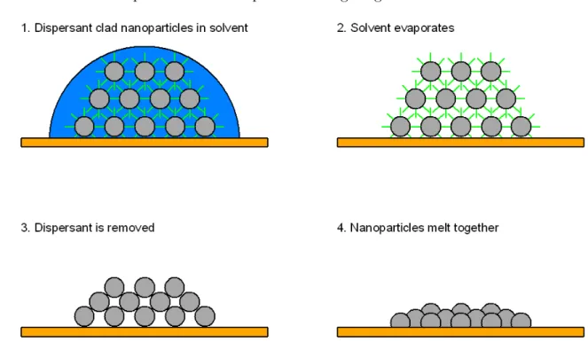
In sintering phase the ink deposited on a substrate becomes conductive. The disper-sion agent is removed from the surface of the nanoparticles and the particles merge together to form a conductive structure. The most common method for sintering is heat transfer by a convection oven [18] [19]. Recently available copper nanoparticle inks require photonic sintering, e.g. laser [20], to speed up the sintering process to avoid particle oxidation.
2. Flexible Electronics 15 Overview of the ink drying and sintering process is presented in gure 2.8. As ink is deposited on the substrate the solvent evaporation begins. Most of the solvent is usually evaporated during printing, depending on the substrate temperature. When the printed structure is transferred to an oven, the remaining solvent evaporates. When enough heat is transferred to the structure the dispersant is removed from around the nanoparticles and the particles merge together.
Figure 2.8: A simplied overview of the ink drying and sintering process.
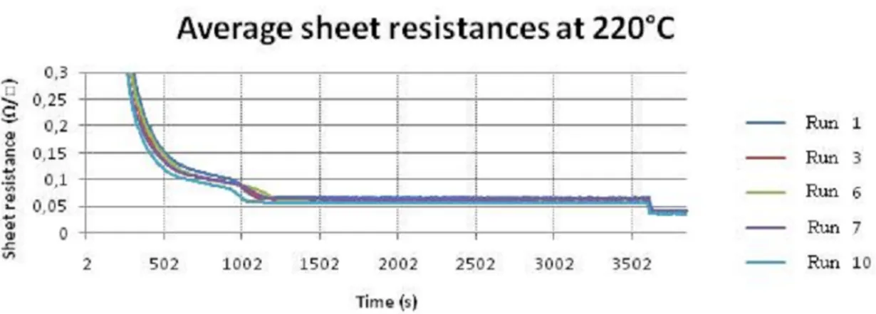
Harima NPS-J silver nanoparticle ink was used in this thesis work. The properties of this ink will be discussed later. The sintering time instructed by the supplier for Harima NPS-J silver ink is 1 hour in 220◦C. The sintering of NPS-J silver
nanoparticle ink as a function of time can be seen in gure 2.9. A drastic drop in resistance can be seen within the rst 20 minutes of the sintering. After that the resistance stabilizes. The drop in resistance at 1 hour mark is due to sample removal from the convection oven. The resulting sheet resistance is ca. 0.040 W/. A small knee can be seen right before the stabilization of resistance at about 15 minutes from the beginning of the sintering. The reason for the knee is not certain, but it is suspected to be the point where the dispersion agent is removed from around the nanoparticles and the particles melt together [21].
2. Flexible Electronics 16
Figure 2.9: Square resistance of NPS-J silver nanoparticle ink as a function of time. Re-sistances were measured during sintering from 5 cm long, 300µ m wide lines, which were
placed in a convection oven. Horizontal axis is time in seconds, Vertical axis is the square resistance of the samples. [21]
17
3. DEVICE DESIGN CONVERSION TO INKJET
TECHNOLOGY
A exible printed circuit board (PCB) of a mobile phone was decided to be manu-factured with inkjet printing technology as a technology demonstrator. The original product design was modied due to the change of manufacturing technology. New materials were selected and the original design les were modied the iTi inkjet printer for PCB manufacturing and for the Corelase X-LASE laser for via drilling. In this chapter the ex-module properties are presented and the material selection and the design modications are discussed. The idea is to explain the design con-siderations from the point of view of inkjet technology.
3.1 Device Description
In this section the features of the exible PCB module are introduced. Demands placed by the original design are discussed and viewed from the point of view of printable electronics.
A exible PCB was selected as a demonstrator device to be manufactured by the means of printable electronics. The selected exible PCB is a part of a basic mobile phone. The mobile phone has a sliding mechanism and a exible PCB is needed to connect the display, keyboard and earpiece to the main PCB of the phone. The display, earpiece and keyboard are located on the slider bar and the exible PCB is needed to make the connection between the moving slider and the motherboard. Connection is made through holes in the slider frame and the motherboard. The ex-module and the slider mechanism can be seen in gure 3.1.
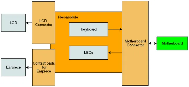
The exible PCB has two connectors, two stiener plates beneath the connector areas, a keyboard and some passive SMT components which include LEDs for illu-minating the keyboard. The functional parts of the ex-module and their interfaces to the actual PCB are described in gure 3.2.
3. Device Design Conversion to Inkjet Technology 18
Figure 3.1: Flex-module, sliding mechanism and the motherboard of the mobile phone. On the left side gure (A) the sliding mechanism is closed and on the middle image (B) the sliding mechanism is open. On the rightmost image (C) the connection of the ex-module and the motherboard can be seen.
Figure 3.2: Interface diagram of the ex-module. The brown boxes represent the connectors and connection pads of the ex-module. The blue boxes represent the main functional parts connected to the exible PCB. The green box represents the motherboard. Arrows point out the direction in which data is transmitted.
3.1.1 Display and LEDs
The exible PCB connects the LCD display to the motherboard of the mobile phone. The display is connected to the motherboard with 13 data lines, including write line, reset line, data/command select line, read line and eight data lines. There are also routings for grounding and supply voltages. The smallest line widths and gaps used in the display control lines in the original design are 75µm wide. The control lines run in an u-shaped curve between the two connectors in the ex module (see gure 3.3). The approximate length of the traces is about 12 cm. The manufacturing and performance of the display control lines was expected to be one of the challenges when transferring the design to inkjet technology, as the resistance of the lines was expected to rise compared to the original design. The performance of the inkjetted
3. Device Design Conversion to Inkjet Technology 19 display control lines was tested and will be discussed later in the testing chapter.
Figure 3.3: Display control line routings on the ex module.
The exible PCB has two LEDs for illuminating the keyboard. LEDs are placed on the top layer of the board and on the opposing side there are resistors and varistors. The resistors are used as ballast resistors for the LEDs and varistors are used for controlling the light-up time and dimming time of the LEDs.
3. Device Design Conversion to Inkjet Technology 20
3.1.2 Keyboard
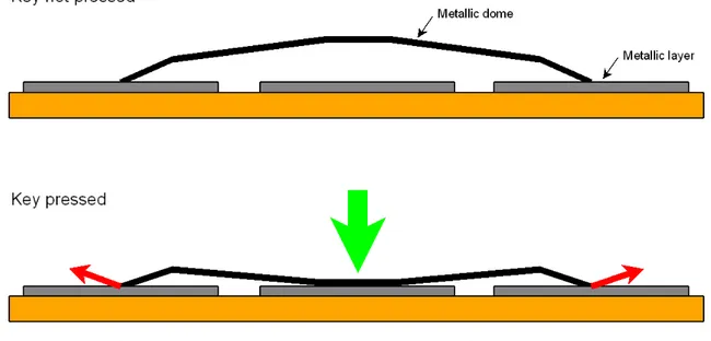
This mobile phone has two keyboards. The keyboard on the ex-module is used for answering calls, ending calls and moving around in the menu. The power-on-key is also on this power-on-keyboard. The other power-on-keyboard is on the motherboard and it is used for the input of numbers and characters. The keyboard in the ex-module has nine keys. The keyboard is constructed by placing an adhesive sheet with metallic domes on top of the printed circuit board. The dome is pressed against the circuit board to create a galvanic contact between separated areas. Data from the keyboard is transmitted to the motherboard by seven data lines which include two lines for reading rows, six lines for reading columns and one line for the power-on-key. The keyboard construction can be seen in gure 3.4.
Figure 3.4: Dome keyboard of the exmodule.
One design concern at the beginning of the project was the endurance of inkjetted keyboard pads. The concern was if the mechanical stress caused by the metallic domes would wear out the inkjetted layer as the inkjetted conductive layer is only a few micrometers thick. When the metallic dome is pressed it connects the separate pads. During this transformation minor friction is inicted on the outer rim of the dome. On a standard PCB this is not a problem as the metallic is much thicker than an inkjetted metallic layer. However, it was unclear if an inkjetted metallic layer would withstand this kind of long term mechanical stress. Now it can be said that during the testing phase no defects caused by mechanical stress of the keydomes were observed, though the long term eects remain unknown.
3. Device Design Conversion to Inkjet Technology 21
Figure 3.5: Mechanical stress caused by the dome movement.
3.1.3 Earpiece
The exible PCB also connects the earpiece component to the motherboard. The earpiece component is connected to the PCB by a plastic holder which pushes the component against the PCB surface. There are four connection pads on the compo-nent to be connected to the PCB and one pad for grounding the compocompo-nent in the metal slider. Two signal lines are directed from the motherboard through the exi-ble PCB to the earpiece component. There are ltering components on the exiexi-ble PCB for the removal of noise from the signal lines.
3. Device Design Conversion to Inkjet Technology 22
3.2 Material Selection
One of the rst steps of the design phase of the inkjetted exible PCB prototype was the material selection. Overview of the material selection can be seen in table 3.1. The substrate material and nanoparticle ink were selected at the start of the project. Other materials were selected during the design and manufacturing of the rst inkjetted prototypes. The cheapest possible materials were not selected yet for prototyping. It was decided that the building of the inkjetted prototype was rst to be carried out with familiar materials.
Purpose Material
PCB interconnections Harima NPS-J silver nanoparticle ink
Substrate material Kapton polyimide lm
Component attachment (electrical) Creative 124-08C
Component attachment (mechanical) Epotek U-300 underll epoxy
Conformal coating Hysol PC28 STD Spray-on varnish
Striener plate material Kapton polyimide lm
Table 3.1: Material selection of the inkjetted exible PCB prototype.
The selected conductive nanoparticle ink was Harima NPS-J. Harima NPS-J ma-terial properties can be seen in table 3.2. Harima NPS-J ink was selected because of its good performance and reliable jetting (Harima NPS-J has a Z value of 2.68 [12]). NPS-J properties Particle Size 8-15 nm Metal Content 62-67 wt% Solvent Tetradecane Viscosity 7-11 mPa·s Specic Gravity 1.8-2.2 Sintering 220◦C(60 min.) Specic Resistance 3µW·cm Thickness Shrinkage 80-85 % Table 3.2: NPS-J properties. [22]
The selected substrate material was Kapton HN-200 polyimide lm. It was se-lected because it has been previously used when making inkjetted applications with Harima NPS-J ink. The main reason for the use of Kapton polyimide lm is the high sintering temperature of Harima NPS-J ink. Kapton has a good heat stability and it can withstand temperatures up to 400◦C. The selected lm thickness was 50µm. Some properties of Kapton HN lm are listed in table 3.3.
3. Device Design Conversion to Inkjet Technology 23 Kapton HN-200 properties
Usable Temperature Range −269◦C- 400◦C
Melting Point None
Thermal Coecient of Linear Expansion 20 ppm/◦C
Shrinkage (30 min at 150◦C) 0.17%
Dielectric Constant 3.4 (1 kHz)
Table 3.3: Kapton HN-200 properties. [23]
Isotropically conductive adhesive was used in the inkjetted version due to the in-compatibility of inkjetted circuits and soldering [24]. The selected ICA was Creative Materials 124-08C. 124-08C is a syringe dispensable, heat cured, exible, silver-lled epoxy adhesive. This ICA was selected because of its relatively fast heat curing time and exibility. 124-08C material properties can bee seen in table 3.4.
Creative Materials 124-08C properties
Volume Resistivity 0.0002 to 0.0004 W·cm
Thermal Conductivity 6.5 W/mK
Glass Transition Temperature (Tg) 120◦C
CTE below Tg 33∗10−6 in/in/◦C
CTE above Tg 84∗10−6 in/in/◦C
Tensile Shear Strength 1500 psi
Specic Gravity 2.6
Useful Temperature Range −55◦C to200◦C
Thermal Stability Good to300◦C
Table 3.4: Creative Materials 124-08C ICA properties. [25]
ICA joints have a fairly poor mechanical strenght compared to solder joints. A exible PCB places high demands on the strenght and quality of the component joints. The mechanical strength ICA component joints to the PCB was enhanced by surrounding the ICA attached components with underll epoxy material. The selected epoxy material was Epotek U300. Material properties of the used underll material can be seen in table 3.5.
3. Device Design Conversion to Inkjet Technology 24 Epotek U300 properties
Volume Resistivity 0.0002 to 0.0004 W·cm
Thermal Conductivity 6.5 W/mK
Glass Transition Temperature (Tg) 120◦C
CTE below Tg 33∗10−6 in/in/◦C
CTE above Tg 84∗10−6 in/in/◦C
Tensile Shear Strength 1500 psi
Specic Gravity 2.6
Useful Temperature Range −55◦C to200◦C
Thermal Stability Good to300◦C
Table 3.5: Epotek U300 Underll Material properties. [26]
3.3 PCB Layout from Gerber to Bitmap
The original design les from the manufacturer were given in Gerber format. The received les included top and bottom side PCB layouts along with via drill les and component placement les. The top and bottom PCB layout les were modied for the iTi inkjet printer. Files were converted from Gerber format to TIFF format and modications were made to the converted TIFF les. Overall description of the circuit layout les conversion process is presented in gure 3.7.
Figure 3.7: PCB layout conversion process.
3.3.1 Changes to Original PCB Layout
The iTi inkjet printer uses TIFF images as input les. The printed le is selected in the iTi inkjet printer XY-stage control software and the le resolution is selected in process (print plate x-axis) and cross-process (print plate y-axis) direction. The resolution in the cross-process direction can be selected from 50 dpi to 5050 dpi with 50 dpi increments. The resolution selection in process direction can be freely selected but after setting of resolution the control software rounds the selected resolution to a suitable resolution for the hardware. The rounding is done because imperial units system is used to control the hardware. When a 5050 dpi resolution is selected in process direction iTi control software rounds the number to 4884.615 dpi. This means that the printed pixel is bit longer in process direction than in cross-process direction. The pixel width in process direction is the length of one inch divided by
3. Device Design Conversion to Inkjet Technology 25 the resolution in process direction, i.e. amount of pixels per one inch (see equation 3.1).
0.0254 m
4884.615 = 5.20 µm (3.1)
And in cross-process direction the pixel height is the length of one inch divided by the resolution in cross-process direction, i.e. amount of pixels per one inch (see equation 3.2).
0.0254 m
5050 = 5.03 µm (3.2)
The error in the pixel process dimension is the intended pixel width substracted from the actual width (see equation 3.3).
5.20 µm−5.03 µm= 0.17 µm (3.3) In high resolutions as in 5050 dpi this error accumulates to a signicant amount. The generated TIFF image had 16986 pixels in process direction and 7800 pixels in cross-process direction. With 0.17 µm error in the processing direction per pixel, the total error in the image can be calculated by multiplying the error per pixel by the amount of pixels in the image process direction (see equation 3.4).
16986 pixels×0.17 µm
pixel = 2.9mm (3.4)
To compensate the rounding error in iTi printer the original Gerber les were scaled shorter in process direction before conversion to bitmap images so that with the XY-stage control software's rounding error the image would realize to be in the original dimensions. The scaling factor can be calculated by dividing the resolution given by iTi's software with the intended resolution (see equation 3.5).
4884.615 dpi
5050 dpi = 0.967 (3.5)
After the scaling in process direction the line widths were trimmed so that the line widths in the inkjetted design would result in about same line widths as in the etched version of the circuit. The actual inkjetted lines are wider than on the bitmap le because the drops on a substrate have a larger diameter than the size of pixels in a bitmap le. For this reason the interconnection lines in the Gerber layout le were made thinner.
The line widths in the Gerber-le were redened by using equation 3.6. The symbols and origin of equation 3.6 are explained in gure 3.8. The basic parameters needed for the estimate are inkjetted drop diameter (d), pixel size in the used bitmap resolution (Wpixel) and the desired line width (W). The line widths in the Gerber le
3. Device Design Conversion to Inkjet Technology 26 (Wdesign) need to be set so, that when the Gerber le is converted to bitmap-form,
the traces will have the desired amount of pixels widthwise. This estimate is best applicable when the printed drops remain separate after printing i.e. in a stacked coin-like structure. The estimate can be used for more uniform lines also, but one needs to be sure that no over wetting is taking place during printing.
Wdesign =W −d+Wpixel (3.6)
Figure 3.8: Method for estimating line widths in a layout design le. A three pixel wide line is used as an example.
3. Device Design Conversion to Inkjet Technology 27
3.3.2 Background for Bitmap Masking Algorithm
Inkjet technology places special demands on the design phase. Some of these issues, e.g. line widths, can be taken into account when designing the circuit in vector format, as discussed in the previous section. Some phenomena related to inkjetting need to be taken into account after transferring the circuit design into bitmap format. In this section these phenomena are pointed out along with the introduction of an image masking algorithm which aims to take these phenomena into consideration. Methods for controlling drop placement accuracy, deposited ink amount and drop placement sequence by modifying the bitmap image are introduced.
Image le resolution determines how accurately drops are placed on the substrate. The most accurate resolution with iTi XY 2.0 printer is 5050 dpi and this resolution was used when printing the layout. High resolution was chosen because of the high precision needed for drop placement. A smaller resolution would be sucient from ink quantity point of view, but it would place restrictions on drop placement accuracy. For example, in 800 dpi resolution the drop spacing would be ca. 32 µm. This would cause signicant placing error in a design le where the smallest line widths and gaps are around 75 µm. At 5050 dpi the spacing of adjacent drops is about 5µm. This means that the position of an individual drop can be determined with 5 µm accuracy on the substrate. However, with 5050 dpi the drop spacing is very small compared to the drop size on substrate. Without any surface treatment a Harima NPS-J drop on Kapton Polyimide is about 90 µm in diameter when the print plate is heated to70◦Cand a Spectra SQ jetting assembly is used. While high
accuracy can be achieved using 5050 dpi the short drop spacing causes line bulging or ooding easily. Flooding and bulging phenomena are related to the amount of ink deposited on the substrate per area, i.e. drop density, and the time delay between the deposition of adjacent drops.
Another challenge related to achieving good print quality is related to drop place-ment, i.e., the way in which the printhead deposits the drops on a substrate. Due to the operation of the printer the adjacent drops are deposited dierently in cross-process and cross-process direction. The time interval between adjacent drop deposition in process direction and cross-process direction is not the same. This easily leads to non-uniform print quality. To understand the problem one needs to understand the operation of the printerhead during printing (see gure 3.9). The printplate moves underneath the printhead in process direction and the printhead deposits drops on surface. After one sweep the plate moves back and makes a microstep for the next row of pixels to be printed during the next sweep. This sequence is carried out several times until the print plate has moved the length of the nozzle spacing in cross-process direction. Due to the operation the time interval between
3. Device Design Conversion to Inkjet Technology 28 adjacent drops deposited in process direction (∆t1 in gure 3.9) is usually around
few hundred microseconds and few seconds in cross-process direction (∆t2 in gure
3.9).
Figure 3.9: Printhead operation during printing. ∆t1 is the time interval between two
adjacent drops deposited in process direction. ∆t2is the time interval between two adjacent
drops deposited in cross-process direction.
Example of non-uniform print quality is given in gure 3.10. The picture is taken from one of the early printing trials made with the ex module layout. Adjacent drops in process direction are formed as one continuous line unlike in the curve, where drops on dierent rows can be seen separately. The line formed by adjacent drops in process direction is uniform but it is also wider than in the curve where drops remain separate.
The problem with making uniform lines is to control the drop deposition so that the solvent has sucient time to evaporate. Drop deposition delay, drop spacing and substrate temperature aect the inkjet-printed structure formation. If adjacent
3. Device Design Conversion to Inkjet Technology 29
Figure 3.10: Example of poor, non-uniform print quality. 1200dpi bitmap image le on the left.
drops are deposited too close to each other or in a too fast rate, bulging or ooding will occur. The relation between drop deposition delay, drop spacing and printed structure morphologies is roughly explained in gure 3.11. As previously stated, the delay between adjacent drop deposition on process direction and cross-process direction is not the same. This places challenges on forming uniform lines in process direction and cross-process direction.
Figure 3.11: Relation between drop delay, drop spacing and structure formation. a) isolated drops, b) scalloped line, c) uniform line, d) bulging, e) stacked coins. [27]
3.3.3 Bitmap Masking Algorithm
A digital bitmap masking algorithm was developed to solve problems related to drop placement accuracy, deposited ink amount and drop deposition sequence. The masking algorithm was developed somewhat through trial and error during the lay-out printing tests of the ex module. Many major and minor tweaks were made
3. Device Design Conversion to Inkjet Technology 30 along the way to make the algorithm work with the selected materials and the used circuit layout. The circuit layout les were converted from vector format to bitmap format in 5050 dpi resolution. The the converted images were masked by a bitmap mask. The mask is constructed as follows (see gure 3.12). A pixel formation is placed in a 37 by 37 pixels element and it is tilted in order to place adjacent pixels in dierent rows. Pixels are placed ca. 31µm from each other. This corresponds approximately with the drop spacing in 800 dpi resolution. Another similar mask layer is placed within the pixel element to enable sucient ink amount and to even out the pixel distribution within the mask. Thus one printed layer using this mask is equivalent to two layers printed in 800 dpi resolution in ink quantity.
Figure 3.12: Construction of the used image masking pattern.
The masking algorithm masks most of the dark pixels white to lower the amount of ink deposited on the substrate. This way the drop placement accuracy of 5050 dpi resolution can be attained while deposited ink amount is also controlled. The printing sequence using the masking algorithm is presented in gure 3.13.
Figure 3.13: Image construction by using the masking algorithm.
3. Device Design Conversion to Inkjet Technology 31 row is greater than the ink drop diameter on the substrate. Due to this, the drops that are printed on the same sweep do not overlap and the drops are allowed to dry individually. If the drops are to be connected, it will happen with the drops printed on the next couple of rows. The drop delay between adjacent drops is now roughly in second scale both in process and cross-process directions. This leads to a stacked coin like structure all around the inkjetted circuit while bulging and ooding phenomena have been eliminated. As a conclusion dierent design phases are presented in gure 3.14 along with examples of the circuit layout and the inkjetted circuit in its nal form.
Figure 3.14: Phases of the layout design process and inkjet printed circuit. The used image is a close up of the originally 75µm wide traces in the layout.
32
4. PRINTED FLEXMODULE ASSEMBLY
In this chapter the assembly process of the demonstrator device is described and the various assembly methods and devices are introduced. The goal is to go through the assembly process in detail and give the reader a conception of the steps needed to manufacture a product by the means of printable electronics. However, it is important to keep in mind that the assembly process is dependant on the product requirements and some of the steps described in this chapter might not be needed for another product, while some other steps may need to be applied. Overview of the manufacturing process can be seen in gure 4.1.
4.1 Kapton Polyimide Preheating
The rst step of the assembly process was preheating of Kapton lm. Preheating on Kapton polyimide is needed because of the shrinkage of Kapton in oven during the sintering of NPS-J silver ink. The relative shrinkage of 50 µm thick Kapton has been determined to be 0.22 % in the horizontal direction and 0.11 % in the vertical direction of the Kapton lm, when Kapton is heated for 60 minutes in
220◦C. Horizontal direction is the direction in which Kapton is rolled into a roll.
Preheating of Kapton was decided to be used because the assembly process con-tains separate heating processes. Without preheating the shrinkage would cause errors in the design dimensions between the sintering of top and bottom layers of the exible PCB. The PCB design le is about 81 mm in length and 40 mm in width. In the worst case scenario with 0.22 % shrinkage would result in about a
170 µm error in the length of the PCB. While it can be argued if preheating was necessary for this specic application, it was decided to be used as a precaution to accumulate as little dimensional error as possible. Kapton was precured for 15 minutes in 220◦C. This was noticed to be sucient to eliminate the eects caused
by shrinkage of Kapton.
Thinking from a manufacturing point of view, eliminating the need for substrate preheating is desirable. As discussed, the need for substrate preheating in this application arose because of the substrate shrinkage during the sintering of the rst conductive layer. Substrate shrinking causes dimensional error between the rst conductive layer and the second conductive layer. This can be seen as a mismatch of dimensions when aligning the rst and second conductive layers. It is signicant
4. Printed Flexmodule Assembly 33
4. Printed Flexmodule Assembly 34 in this application because the pad coordinates must match. However, the via pad sizes allow a small dimensional mismatch as the diameter of the pad is about600µm. It could be possible to eliminate the need for substrate preheating in the design phase or in the assembly phase. One way of compensating the dimensional error caused by substrate shrinking is to scale the rst inkjetted layer larger so that it would shrink back to its intended size with the substrate during the rst sintering cycle of the assembly. Other way would be to combine the sintering phases of top and bottom conductive layers into one sintering phase. This would mean that after printing the rst conductive layer is dried but not sintered during the printing of the second conductive layer. Unsintered NPS-J withstands some amount of handling on polyimide, but bending the substrate much will result in separating the ink from the substrate. Therefore ipping the substrate over during assembly while having unsintered ink on it might be dicult to carry out.
4.2 Laser Processed Vias and Module Outline
The via cutting and module outline cutting was done in the same phase with a picosecond scale pulse laser. The laser has 2 W output power and it operates in 1064 nm wavelength. The laser uses a mirror scanner module (see gure 4.2) to control the laser beam movement to create patterns on a substrate. Focus depth and planar translation are controlled with a three-axis micrometer table. The via drill le from the original design was used to create the processing le for X-lase laser. Via holes were replaced by circles with a diameter of 150 µm.
The module outline was partially cut out from the substrate, but it was left intact at some points (see gure 4.3). This way the module remained attached to the substrate for the entire production phase. This was helpful when attaching the substrate to iTi inkjet printer vacuum table as experience showed that a entirely cut module would not stay at on the vacuum table. Align marks for the alignment of inkjetted conductor layers were made at each end of the laser cut design. Due to the small processing area of the scanner module (5.5cm2) the processing had to be done in two parts. First the other end of the layout was processed, then the substrate was moved 4 cm and the rest of the layout was processed. Due to small oset between the micrometer table translation axes and scanner module beam movement axes, an oset vector was visually determined to be used in the laser scanner control le to correct the placement error. Due to the scanner head operation and the large processing area, pincushion and barreling eect if the processed pattern was observed. Pincushion and barreling eects cause curvature of straight lines in the edges of the processing area. This also aected the coordinates of the via holes, which needed to be manually corrected, so that they would match the routing conductive layers later printed with the inkjet printer.
4. Printed Flexmodule Assembly 35
Figure 4.2: Sample processing with Corelase X-Lase.
4. Printed Flexmodule Assembly 36
4.3 Inkjetted Circuit Board
The conductive layers of the PCB were made by iTi inkjet printer (see gure 4.4). The equipment consists of the printer and the controller units for the printhead and XY-table. Separate software and control units are used control the XY-table and the Spectra printhead to produce inkjetted patterns. A Spectra SQ-128 jetting assembly was used in the Spectra printhead.
Figure 4.4: iTi inkjet-printer and control module.
The temperature of the printhead can be controlled to obtain optimal ink jetting conditions. Ink jetting can be tuned also by controlling the ring voltage pulse am-plitudes and pulse waveform. Ink behavior on substrate is controlled by adjusting the substrate temperature and printing speed. Printing parameters can be opti-mized by using a drop watcher device. The printing parameters used to print the conductive layers of the ex module are listed in table 4.1. Before printing the sub-strates were cleaned with isopropanol and a 1% EGC-1720 surface treatment was made. After printing the samples were sintered in 220◦C for 60 minutes.
With optimized printing parameters and the image masking algorithm the inkjet-ting of the layout was possible. In the early trials when the layouts were printed without the masking algorithm the print quality was not good enough for this spe-cic layout with the used equipment. Example of the print quality achieved with the masking algorithm can be seen in gure 4.5
4. Printed Flexmodule Assembly 37
Printing parameters
Piezo pulse amplitude (V) 45
Pulse rise time (ms) 8
Pulse width (ms) 2
Pulse fall time (ms) 2
Printhead temperature (◦C) 45 Print plate temperature (◦C) 70 Printing speed (mm/s) 30
Table 4.1: Printing parameters used to print the conductive layers of the ex module.
Figure 4.5: Example of ne pitched traces in the layout. The thinnest traces are about90
4. Printed Flexmodule Assembly 38
4.4 Component Attachment
The component attachment was done with ICA and two component epoxy. ICA was used to make the electrical connections between the components and the circuit and epoxy was used to enhance the durability of the mechanical joint between the component and the substrate. Overview of the deposition process is presented in gure 4.6. ICA and the epoxy material were dispensed by a handheld pneumatic uid dispenser so that the amount of dispensed material could be controlled by the pneumatic pulse length. Components were placed by hand or by Fineplacer component placement tool. The ICA joints were cured in a convection oven for 15 minutes in 150◦C. After the ICA curing two-component epoxy material was
deposited around the components to improve the mechanical joint of the component and the substrate. During the assembly of the rst prototypes it was noticed that some components, especially the larger ones, would snap o from the substrate during bending. Epoxy mold around the components helped to keep them attached to the substrate very well. After the epoxy is cured around the components, it acts as a stiener preventing the substrate from bending under the components. This takes the strain o from the components joints and prevents the components from detaching. Epoxy material was also deposited with a pneumatic dispenser and it was cured in a convection oven for 10 minutes in 150◦C.
4. Printed Flexmodule Assembly 39
Figure 4.7: Components attached to an inkjetted ex module using ICA and epoxy mate-rial.
4.5 Conformal Coating
After the component attachment the ex circuit were covered with a spray-on con-formal coating (see gure 4.8). One side was sprayed and allowed to dry and then coating was repeated on other side. This phase of the assembly work was probably the most irreproducible due to the fact that the spraying process is much dependant on the operator. Also pieces of plastic were used to mask out larger areas of the ex circuit, e.g. the connectors which needed to be protected from the spray coating. Even though in the unmasked areas the spray coating resulted in an even layer of coating, around the masked areas there was a lot of variance in the quality of the coating. The other hindsight with this method is that some of the grounding points which connect the ex module ground layer to the metal frame of the phone were left out due to practical reasons. An alternative coating method would be inkjetting the coating layer. By doing this the shape of the coat could be controlled and the masking problems could be avoided. However considering the timetable and due to practical reasons, a spray-on coating was decided to be used, even though it may not be the best alternative. By using a spray-on coating a dielectric layer could be created to protect the traces on the ex module mechanically and also to separate them from the metal frame and other parts of the phone.
4. Printed Flexmodule Assembly 40
Figure 4.8: Flex module after conformal coating.
4.6 Stiener Plates Laser Processing
The exible PCB has two stiener plates under both connectors. Stiener plates are used to reduce the mechanical stress inicted upon the solder joints or in this case ICA joints. The stiener plates proved out to be important while connecting the exible PCB to the motherboard and while connecting the LCD to the exible PCB. The plates help provide even force distribution to the connectors while pressing. The motherboard connector stiener is made out of a 270 µm thick metal plate, which was provided with the components. The stiener plate under the LCD connector was laser cut out of 100 µm thick polyimide lm (see gure 4.9). Both stiener plates were attached to the PCB with an adhesive lm cut out in the shape of the stiener plate.
4. Printed Flexmodule Assembly 41
Figure 4.9: A laser cut stiener plate.
4.7 Mounting the Flexible PCB in the Mobile Phone and
Ini-tial Testing
The inkjet-printed ex modules needed to be veried before sending them for further testing to the manufacturer. Initial testing was done by measuring signal lines for short circuits and open circuits. The rst inkjetted prototype was tested in a self-built support frame where the ex module could be mounted with minimal stress to component connections and the exible circuit board. At this point the ex module was connected to the motherboard and LCD but the phone casing was not tted.
After the electrical functionality of the inkjet-printed ex module prototype was veried a set of new samples were manufactured and mounted inside the actual phones. In order to do this the phones casings were disassembled, the display was disconnected from the ex module and the original ex was disconnected from the motherboard. The circuitry of the ex modules was tested for short circuits and open circuits before installing the ex module inside phone casings. The samples were initially tested by making sure that each phone starts up and that the LCD, keyboard and earpiece were functioning properly. Possibility to make and receive calls was also tested. Eventually 3 working samples were delivered to the manufacturer for further testing.
42
5. ANALYSIS AND PERFORMANCE TESTING
In this chapter the dierences between the original ex module and inkjet-printed ex module are discussed. First the structural dierences are compared followed by a series of electrical tests, which aim to point out any dierences in performance.5.1 Structural Comparison
In this section the dierences in construction of the inkjetted and original ex module samples are pointed out by cross-sectional images. Layer thicknesses, via structures and component connections are discussed.
5.1.1 Layer thicknesses
Inkjet-printed conductive structures are typically only few a microns thick. Very small amount of conductive material is used compared to e.g. etched circuits. The amount of silver ink used for the both sides of the inkjetted ex module is about 110 microliters. This was calculated by multiplying the amount of pixels in the bitmap les with the average ink drop size. With one liter of silver ink ca. over 9000 pieces could be manufactured if all ink is used for making the ex module. The module thicknesses can be seen in gure 5.1. The total thickness of the inkjetted ex module is about 150 µm. The thickness of the original module is about 120 µm. The inkjetted ex module is slightly thicker because of the thicker substrate material and thicker coating layer.
The dierence in conductive layer thicknesses in the inkjet-printed and original ex module can be seen in gure 5.2. In the inkjetted structure the silver ink layer thickness is around 7 µm, which is about one third of the metal layer thickness in the original ex module. In the original ex module the copper layer thickness is about 20µm.
![Table 3.4: Creative Materials 124-08C ICA properties. [25]](https://thumb-ap.123doks.com/thumbv2/123dok/2219513.2718409/30.892.170.811.455.682/table-creative-materials-c-ica-properties.webp)

