DESIGN OF FREQUENCY SELECTIVE LIMITING CIRCUIT
N.H. ALI
Z. ZAKARIA
R. PHUDPONG
,T" International Contercnce on Engineering and !CT (ICE12012) Melaka, Malaysia
4- 6 April 2012
DESIGN OF FREQUENCY SELECTIVE LIMITING CIRCUIT
N.H.Ali
1'a•,
Z.Zakaria
1'b
and R.Phudpong
21 Universiti Teknikal Malatsia Melaka, Malaysia. aEmail: [email protected],
Email: [email protected]
3 National Electronics and Computer Technology Center, 112 Thailand Science Park, Klong Luang, Pathumthani,
12120 Thailand
Abstract-This paper explains the design of frequency-selective limiting circuit. The circuit is typically based on nonlinear matched reflection-mode bandstop resonator. This type of Frequency Selective Limiters achieves fast switching, high-level of power limiting, and flexible channel bandwidth. For single channel limiting, a device with one resonator (first order) produced a band-stop response centred at 2 GHz with 250 MHz of limiting bandwidth, 0 dBm limiting threshold, and 32 dB limiting level and it gave an all-pass response with less than 2.5 dB insertion loss at low RF powers. Multi-resonator filter has been used in order to improve the performance of the device. The prototype will produce intermodulation distortions and response time. Simulated results show an excellent highly selective bandstop performance at high powers with a near all-pass response at low signal powers.
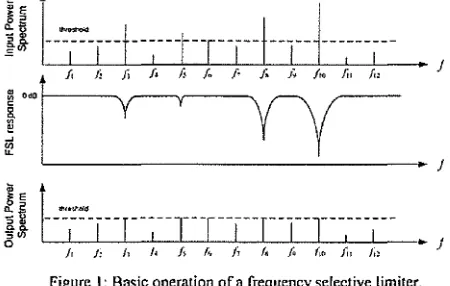
Figure I: Basic operation ofa frequency selective limiter.
II. INVESTIGATION OF M!CROSTRIP TOPOLOGY FOR A
Keywords-Bandstop filters, limiting, microstrip resonators, BANDSTOP RESONATOR
microwave limiters, 11011li11ear filters.
I. INTRODUCTION
Jn microwave application, limiters are located at the front-end of microwave receivers. It functions to protect the sensitive circuitry against large interfering signals. In application of conventional limiters, they make use of shunt PIN diodes where it is placed before the receivers. The drawback of PIN limiters is, it cannot differentiate the received signals in terms of frequency. According to [ 1,2], they respond to the total RF power, attenuating all signals when the accumulative powers exceed the limiting threshold. By attenuating the wanted small signals, therefore they can limit the magnitude of large signals, with a resultant decrease in sensitivity and the interfering signal is removed.
Frequency selective limiter (FSL) functions to limit signals at each individual frequency independently. Basically, this technique can suppressed the interference automatically if the threshold is exceeded, provide equalization and limits the overload signal while maintaining the strength of low level signal. The operation of frequency selective limiter is as shown in Figure 1. In addition, FSL makes use of a series bandstop resonator loaded with a diode limiter where it is placed in a shunt configuration with the receiver's front-end circuit.
In designing a nonlinear bandstop filter, microstrip technology has been used and selection of diode will take into consideration as well. Typically, there are two microstrip components being discussed here, that is distributed bandstop resonators, or a network containing a lumped capacitor and a quasi-lumped inductor. For distributed bandstop resonators, the circuit can be constructed in three ways which are shunt half-wave short-circuit resonator, capacitively coupled resonator and L-shape coupled line resonator. As for quasi-lumped inductor, inductor and capacitor will be involved.
Diode is the most important component in the circuit. The three criteria for the diode selection are ability to operate at microwave frequencies, extremely low variation of the junction capacitance and extremely low junction capacitance and other parasitic.
III. DESIGN OF A FIRST-ORDER NONLINEAR BANDSTOP FILTER
In designing first-order filter, Advanced Design System (ADS) has been used for the simulation. First, it started with designing circuit for schematic simulation. Next, the circuit components in the schematic were transformed to microstrip after obtaining the desired result. After the simulation has been performed, the high-accuracy simulated results and the microstrip layout of the prototype are achieved.
[image:2.597.298.523.159.302.2],3'" International Conference on Engineering and !CT (ICEI2012) Melaka, Malaysia
4 - 6 April 2012
operation, first-order subnetwork and quarterwave transformer (impedance inverters) that functions to allow impedance matching between branch line coupler and subnetwork as shown in Figure 2.
Quarterwave First-order
Transformer Subnetwork
セ@
Input
1
o--I
-J:-
Quadrature IHybrid I =
I
Output セ@
I
f
-b
II =
[image:3.595.314.520.54.207.2]0)
I I®
®
Figure 2 Circuit clements in a first-order nonlinear bandstop filter.
Zo Zo
(Input)(!) (1) {Output}
Zo Zo
(Isolated)
©
Q) (Oulput) [image:3.595.47.282.111.267.2]z, Zn
Figure 3 Geometry of branch-line coupler
Figure 3 shows the basic operation of the branch-line coupler. The matrices of an unloaded branch line coupler for even and odd-mode transmission can be expressed as
[;
セャ@ ]fゥ{セA@
Mセj@
(I)[;
セャ@ ]fゥ{セ@
セ}@
(l)At the output port 2 and 3, the admittance Ye and Y0 are
1
y
=dセN@
+C
=
ェMセᆳ
e bセN@
+A
jセN@-1
y
=
ェKセN@
=-1
0
·y:
+
1y
j L e
(a)
f:;;·:;,_,,;· t.<.t"T,,,
.,
セ[FZ[エbBBGZGNTQG@
i><•..l ZセNLNL@
セNZNエNBA[ZN@
lGセッイ・^@
' .,....,c;i,..,... セセ[LセNLNLNN@ (3)
(4)
.,
:t.:fn:;;A•' .,..v;•..,..
o. s _ _ _
GMNMセセ@
- · - - - -....__ ..._ 12 S11 ,..--:::: _ ___. ,.
·i s|TGMセNN⦅@ NZ\Mセ@
in
.2JJ
"
Oセ@
::s..
I I I]
セ@
\
(
J1
I
I
;
! I
1.0 1.2 1.4 1.6 1.8 20 2.2 2.4 26 2.8 3.0
Frequency (GHz)
Figure 4 (a): ADS layout; (b) Simulation of branch line coupler
Figure 4 shows the ADS layout for first-order filter and
simulated results. It can be observed that S12 and S13 are
at -3dB when all ports matched, power entering port 1 is evenly divided between ports 2 and 3, with a 90° phase shift between these outputs. No power is coupled to port 4 (the isolated port). Thus, the [SJ matrix will have the following form:
0
j
1
0
{sj]セ@
j
0
0
1
I
0
0
j
(5)0
1 j
0
The next part is designing a first-order subnetwork which involved a simple LC bandstop resonator loaded with a
Schottky diode. The choice of L and C value can be vary
depending on Q value. For a high Q, the capacitance should be small and inductance should be large. In this case, L and C values were 30nH and 0.211 pF respectively. Figure 5 shows the LC nonlinear bandstop filter in the form of schematic diagram and the simulated
result when it is loaded with diode.
DC Block
Port 1
Diode
(a)
DC Block
RF Choke
[image:3.595.54.276.225.346.2] [image:3.595.43.533.498.739.2])"'International Conference on Engineering and JCT (!CEI2012) Melaka, Malaysia
4- 6 April 2012
0 a
-S I
RFpowor
a.:odSm
b = S dBm
e-=10d8m d=15dBm
e zzto<!:Btn
f=-25<lBm
g;3QC:Bm
1.0 1.2 1.4 1.6 1.8 2.0 22 2.4 26 28 3.0
Frequency (GHz)
(b)
Figure 5(a); An LC bandstop filter loaded with a diode.; (b) Simulation of an LC bandstop filter loaded with a diode
Since the construction of the bandstop resonator is based on microstrip circuit, thus, the LC circuit is transformed to a capacitively-coupled transmission line resonator as shown in Figure 4(a). The equations involved in the transformation are:
C ' =
-w0Z0
tanB
(6)
(7)
(8)
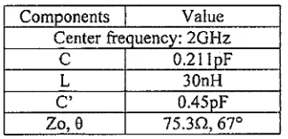
Table 1 shows the transformed value of components
using the frequency of2GHz and has the same Q value.
Table l: Transformed value of LC circuit to a capacitively-coupled transmission line resonator
Components Value
Center frequency: 2GHz
c
0.21IoFL 30nH
C'
0.45pFZo,0 75.3n, 67°
A microstrip bandstop resonator loaded with a diode shown in Figure 6(b ). The interdigital capacitor is a microstrip lumped component must be at least ten times smaller than the operating wavelength to get insignificant phase variation and allowed several design techniques
used at low RF frequencies, which were not practical at
microwave frequencies, to be successfully applied up to
30 GHz. A high impedance short-circuited quarter
wavelength transmission line can be used as an RF choke.
It is seen as an open-circuit by the RF signals, but as a
short-circuit by DC signals.
ln,erdigilal C3pocitar
SchoUky diod•
Input
_L (a)
Short..circuited
qunrtetW.3\ll!t: 1lub
lndudiVt'! short·
circuited stub
(b)
I•
Figure 6(a): A transformation of an LC resonator to a capacitively-coupled transmission line resonator; (b) A microstrip bandstop resonator
loaded with a diode
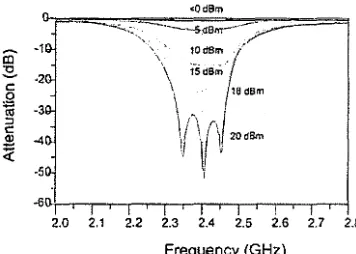
After all components have been integrated, the simulated result of a first-order nonlinear bandstop filter is as shown in Figure 7 where the impedance inverter (K) also has been included in the system in order to match the impedance of the branch-line coupler and subnetwork. Based on this result, it can be seen that when the RF power level less than OdBm, the attenuation is below 2d8. The amount of attenuation will be increasing as the RF power increased. Therefore, attenuation and RF power is directly proportional to each other in first-order bandstop filter. The maximum attenuation is at 32dB for the RF power of20dBm.
<OdBm
PM]エ]]]ZZZZ[[[[[[[[[[[[Z[MZZZ[ZZ[ZNセMMMMMMMM]]]]]]ZZ[[[[[[[ZZZZZZZZZ[[[Z[[[[[ZZ]ゥ@
-> \:.
B(mQセ@
dBmCi)' -10
"C ..._,.
c
0
:g
-20:::i
c
Q)
セ@
-301.6 1.8
\'.
'( 15dBm l
I
18dBmj
20dBm2.0 2.2
Frequency (GHz)
[image:4.595.317.516.59.272.2]2.4
Figure 7 Simulated results ofa first-order nonlinear bandstop filter
IV. THIRD-ORDER NONLINEAR BANDSTOP FILTER
[image:4.595.62.262.61.214.2] [image:4.595.67.266.316.426.2] [image:4.595.302.531.458.631.2] [image:4.595.71.233.491.569.2]· 3'" International Conference on Engineering and !CT (ICEl2012) Melaka, Malaysia
. 4-6 April 2012
subnetwork component. Figure 8 shows the third-order bandstop filter subnetworkand the transformed equation can be calculated as follows:
Figure 8 Lumped circuit of a third-order bandstop filter sub-network.
C
::::: BW.C
new
2
·"J -.rl' 2 0Z
()(9)
L
=
Zo
new
27rBW.C
(10)R
-
zo
new -
G(Q2
+
l)
(11)(12)
According to [3], the equation for S11 ofa one-port lossy
ladder network in Figure 6 can be written as
s (
a)=
rr"
pa- jcoser
II
p, r=Ipa-
jcos(cos-l(a)+eJ
(l3}where;
]'7[
B =
-rn+
l'
a
is a constant which determines the ripple level,n is the order of the subnetwork
Therefore, the admittance of shall be expressed as
(14)
In third-order filter, the response also varied with RF power levels. From Figure 9, RF power level less than 0 gave a near all-pass response with an attenuation of2dB. The attenuation will keep increasing gradually as the RF power level increased.
<OdBrn
2.0 2, 1 2.2 2.3 2.4 2.5 2.6 2.7 2.8
[image:5.602.302.480.53.180.2]Frequency (GHz)
Figure 9 Simulated results of a third-order nonlinear bandstop filter.
The comparison of the first and third-order prototypes can be made based on the design and response of the frequency and transient. In terms of design, reflection mode configuration forms the basic design of the first and third-order prototypes where they are differed by the design of the sub-networks. While in the aspect of multiple signal response, the third order intermodulation products of the third-order prototype produced higher output powers than that of the first-order. Higher intermodulation distortion is generated due the third-order circuit having more non-linear elements than the first-order circuit.
V. CONCLUSION
In conclusion, the circuit analysis as well as simulation of the Bandstop Limiter has been discussed. The prototype of a first order bandstop filter, based on a reflection mode filter, gave high performance limiting characteristics that is useful in the application of Frequency Selective Limiting. In addition, it is possible to cascade Bandstop Limiter modules for wideband operation since the
Bandstop Limiter is matched ( S11 = 0 ). The circuit
sustains the strength level of small signals while compresses large signals. Therefore, significant reduction in the signal dynamic range is achievable.
REFERENCES
[I] J.D. Adam, and S.N. Stitzer, "Frequency-Selective limiters using nonlinear bandstop filters," IEEE Trans. MTT, vol. 57, no. 1, pp. 157-164, 2009.
[2] R. Tan, "A limiting filter," Microwave Symposium Digest, IEEE MTT-S International, pp. 1275-1278, vol.3, Jul. 1991.
[3] J. Rhodes, "Microwave reflection filter including a
[image:5.602.47.283.95.177.2]