Published by Canadian Center of Science and Education
Low Power Operational Amplifier in 0.13um Technology
M. I. Idris1, N. Yusop2, S. A. M. Chachuli3,M.M. Ismail4, Faiz Arith5 & A. M. Darsono6 1
Faculty of Electronics & Computer Engineering, Universiti Teknikal Malaysia Melaka, Hang Tuah Jaya, 76100 Durian Tunggal, Melaka, Malaysia
Correspondence: M. I. Idris, Faculty of Electronics & Computer Engineering, Universiti Teknikal Malaysia Melaka, Hang Tuah Jaya, 76100 Durian Tunggal, Melaka, Malaysia. Tel: 60-190-6555-2093. E-mail: [email protected]
Received: June 26, 2014 Accepted: July 14, 2014 Online Published: November 23, 2014
doi:10.5539/mas.v9n1p34 URL: http://dx.doi.org/10.5539/mas.v9n1p34
The research is financed by Univeristi Teknikal Malaysia Melaka (UTeM).
Abstract
Low power is one of the most indispensable criteria in several of application. In this paper a low power operational amplifier consists of two stages and operates at 1.8V power. It is designed to meet a set of provided specification such as high gain and low power consumption. Designers are able to work at low input bias current and also at low voltage due to the unique behavior of the MOS transistors in sub-threshold region. This two-stage op-amp is designed using the Silterra 130nm technology library. The layout has been draw and its area had been calculated. The proposed two stage op-amp consists of NMOS current mirror as bias circuit, differential amplifier as the first stage and common source amplifier as the second stage. The first stage of an op-amp contributed high gain while the second stage contributes a moderate gain. The results show that the circuit is able to work at 1.8V power supply voltage (VDD) and provides gain of 69.73dB and 28.406MHz of gain bandwidth product for a load of 2pF capacitor. Therefore, the power dissipation and the consistency of this operational amplifier are better than previously reported operational amplifier.
Keywords: op-amp, two-stage, miller capacitor, gain, ICMR, PSRR, CMRR, slew rate, low power, power dissipation
1. Introduction
The operational amplifier (op-amp) is a core part in designing an analog electronic circuitry and mixed signal systems[1][2]. There are various levels of complexities when designing an operational amplifier and thus make it a versatile device that ranging from a dc bias generation to a high speed amplifications to filtering[3][4][5]. Operational amplifier is widely used in electronic devices today as it being used in industrial, scientific devices and in a vast array of consumer.
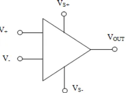
Figure 1. Symbol of op-amp
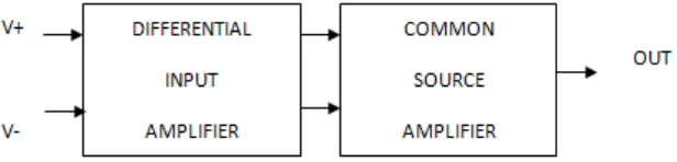
input represent by a positive sign (“+”) and both of its have a very high input impedance. The third terminal of an operational amplifier is output port where it could be both sinking and sourcing either a voltage or a current. The difference between the two signals being applied to the two inputs of an operational amplifier is called the amplified output signal. Due to this, a differential amplifier is generally used as the input stage of an operational amplifier and hence an operational amplifier is also called a DC-coupled high-gain electronic voltage amplifier. Block diagram of an operational amplifier is described in Figure 2 where differential input amplifier is a first stage with two input voltage and common source stage as the second stage.
Figure 2. Block diagram of two-stage op-amp
A low power operational amplifier gives advantages in many applications owing to prolongation of battery life and thus makes it suitable for portable devices. In analog devices product development, it offers high power efficiency without compromising the speed, noise and precision. Low power op-amp is widely used as a bio-potential amplifier where it is used to amplify and filter extremely weak bio-potential signals[6]. In industrial sections, it is widely used in the usage of barcode scanner.
Nowadays, the need on smaller size chip with very small power dissipation has increased the demand on low power design. But the obstacles on designing a good performance of a low power op-amp are on operating with power supplies that is smaller than 1 Volt, on getting an ideal characteristic of op-amp specification and on designing a circuit with the same or better performance than circuits designed for a larger power supply.
This paper is organized as follows. Section II describes the proposed schematic design being considered. In Section III, the design method is presented. Section IV provides the simulation results, performance comparison, and discussions. Finally, our conclusions are given in Section V.
2. Proposed Schematic and Method
2.1 Proposed Schematic Two-Stage Op-Amp
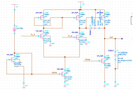
The first block is an input differential amplifier and it was design to provide very high input impedance, a large CMRR and PSRR, a low offset voltage, low noise and also high gain [14-16]. The output is single ended so that the rest of the op-amp did not contain symmetrical differential stage and since the transistors is operating in the saturation region, there is an appropriate dc voltage difference between input and the output signals of the input stage.
Figure 3. Proposed two-stage circuit design
2.2 Design Specification
Before start the design, there are several specification need to be assumed or take into consideration. The specifications are:
This consideration will be used to determine the width and length of the transistor. Based on the proposed schematic in Figure 3, the W/L ratio for M3 and M4 will be found from the max ICMR +, M1 and M2 will be found from the tranconductance gm1 and GBW, the current flow through M5 will be found from the slew rate, M5 and M6 will be found from minimum ICMR -, M6 from gain and the design of M3 and M4, I6 current flow to the second stage is related to the design of M3,M4 and I5, M7 is related to I5 because of the same biasing voltage and lastly the Cc value from phase margin. The length of the transistor value used when involving the two stage op-amp is L ≥ Lmin. Lmin is the technology used which is 130nm. So in this design the length used are either L=1000nm or L=500nm but only 500nm will be used. The 1000nm value will only be used if needed to satisfy the condition required. This large value is used to avoid channel length modulation and also the lambda,
.
The op-amp has been design based on the given step below [7]:
2.3 Design Calculation 1. The length used is 500nm
2. The phase margin specification is 60◦, so the compensation capacitor equation is
Cc ≥ . × CL (19) Cc is compensating capacitance and CL is the load capacitance.
3. The total current or the current flow through M5 is
4. Design of M1 and M2 from the gain bandwidth product (GBW) and the small signal transconductance
I5 is the drain current of M5, VDD is the positive supply voltage, ICMR+ is the maximum input voltage, Vt is the threshold voltage and µpcox is the transconductance parameter.
6. M5 and M6 design from the minimum input voltage range (ICMR-)
VDS ≥ ICMR − − I ncox W L⁄ − Vt (24)
W L⁄ = (25)
7. Design of M7 from gain and design related to M3 and M4
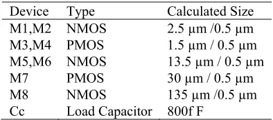
gm ≥ × gm (26) From all step above, the calculated value of different MOSFET is recorded in Table 3-2:
Table 2. Calculated Size of MOSFETs
3. Result and Discussion
The design of two-stage op-amp was simulated based on its different characteristics such as transient, gain, GBW, phase margin, slew rate, CMRR, PSRR, output offset voltage and power dissipation. These characteristics are varied using ICMR of 0.8V and 1.6V. Furthermore, the layout of the designed op-amp was drawn. The different results are presented here.
3.1Transient Analysis
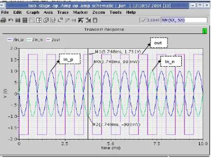
An amplifier is an electronic device that modulates the output of the power supply. This analysis has been used to identify whether the output obtained is greater than the input of differential amplifier. The analysis has been done by connecting both input pair with sinusoidal voltage and dc voltage to VDD and VSS terminal. Figure 4 shows a plot of the two-stage op-amp output voltage VO versus the differential input voltage in_n, in_p. The output obtained is 1.731V, in_p 990mV and -1.731V in_n -990mV.
Figure 4. Transient analysis
3.2 AC Gain and Phase Analysis
This analysis has been done separately for ICMR + and ICMR -. From this analysis the gain, GBW and phase margin can be obtained. The gain is the ratio of the output to the input, GBW is the product of the bandwidth and gain at which the bandwidth is measured and the phase margin is measured to determine the stability of the design. For ICMR+, the gain obtained is 69.73dB, the GBW is 28.406MHz and the phase margin is 60.529. For ICMR -, the gain obtained is 76dB, the GBW is 28.406MHz and the phase margin is 60.252◦.
Figure 6. Op-Amp Gain for ICMR-
3.3 Input Common Mode Range (ICMR)
ICMR is the common mode voltage range. Usually the input-output transfer curve for ICMR simulation is linear and all MOSFETs are operated in saturation region. To measure the ICMR, the negative terminal of the first stage is connected to the output terminal and the positive terminal is connected to the dc voltage with frequency 1 kHz and DC voltage is swept from 0.8V to 1.6V with supply voltage VDD of 1.8V. The input common mode range of this two-stage op-amp slope is 0.982V which is approximately to 1V.
Figure 7. ICMR
3.4 Common Mode Rejection Ratio
Figure 8. Differential Mode Gain
Figure 9. Common Mode Gain
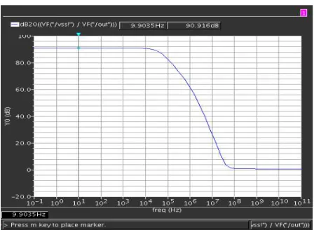
3.5 Power Supply Rejection Ratio
PSRR analysis is used to describe the amount of noise from a power supply that a design op-amp can reject. PSRR is measured with both positive and negative power supply in decibel (dB). For PSRR + the VDD is supply with 1V amplitude, 1.8V of input voltage and 1kHz frequency while VSS is supply with -1.8V. Meanwhile, PSRR- is inversed from PSRR+. The input positive of differential amplifier is connected to the ground while input negative is connected to the output terminal. This condition is same for both PSRR. The PSRR + value obtained is 99.76dB and PSRR- value is 90.916dB.
Figure 11. PSRR-
3.6 Slew Rate
Slew rate analysis is the maximum speed at which an op-amp can charge and discharge its load. Slew rate is measured by connecting input negative to output terminal and input positive is given a voltage pulse supply of 0.8V and 1.6V. The slew rate value is obtained on its rising and falling edge slope. The slew rate obtained is 20V/ s.
Figure 12. Rising Edge
Figure 14. Output offset voltage
3.7 Output Offset Voltage
When the input terminals are connected together, there is a voltage appears at the output of the differential amplifier called the output offset voltage. The output offset voltage value obtain is -1.5V
3.8 Power Dissipation
The power is calculated as the power dissipated by the VDD supply. In Cadence tools, this power dissipation is obtained by clicking the output tools then save all. After that at DC analysis save the DC operating points and done the simulation. The power dissipation value is then obtained by using the result browser. The power dissipation when ICMR+ is 0.3898mW and for ICMR – is 0.3644mW.
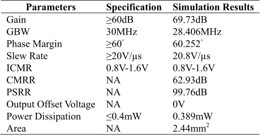
Table 4. Simulation result for low power op-amp
Parameters Specification Simulation Results
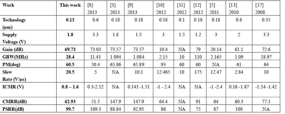
An improved design and a comparative study of low power operational amplifier using a NMOS current mirror as bias circuit is presented in this research. The modified circuit has been designed by using the CADENCE 0.13- m CMOS process. In this research, Designing of op-amps continues to pose further challenges as the supply voltages and transistor channel lengths scale down together with the introduction of each new generation of CMOS technologies. According to the research results, it has been proven that, the circuit is capable of providing a gain of 69.73dB and a 28.406MHz of gain bandwidth product for a load of 2pF capacitor. The results also verify that the modified circuit has CMRR of 62.93dB and output slew rate of 20V/µs. Moreover, the two-stage op-amp has a PSRR+ of 99.76 dB and PSRR- of 90.91dB. The presented op-amp has an Input Common Mode Range (ICMR) of 0.8V to 1.6V and power consumption of 0.389mW. Additionally, the circuit size reduced significantly by using small transistors and capacitors.
Acknowledgements
References
A. and Holberg. (2002 ). CMOS Analog Circuit Design.
Satheesh, B., Dhanalakshmi, N., & Balaji, N. (2012). Design of a Low-Voltage, Low-Power, High-Gain Operational Amplifier for Data Conversion Applications. International Journal of Engineering Research and Applications, 2(3), 1030–1036.
Bhadra, D. (2011). Physical Design Of Low Power Operational Amplifier.
Idris, M. I. B., Reaz, M. B. I., & Bhuiyan, M. A. S. (2013). A Low Voltage VGA For RFID Technology”, Receivers, 2013 IEEE International Conference on RFID-Technologies and Applications, 1-4.
Shang, K. (2008). Design of a Dedicated Miller-opAmp.
Idris, M. I., Shah, Z. M. N., Ismail, M. M., & Rahim, R. A. (2012). Design of a Low Voltage Class AB Variable Gain Amplifier (VGA). Journal of Telecomunication, Electronic and Computer Engineering(JTEC), 4(2), 69-74.
Mohammad A. S. B., Muhammad I. B. I., Mamun B. I. R., Khairun N. M., & Hafizah, H. (2014). Low Voltage and Wide Bandwidth Class AB Variable Gain Amplifier in 0.18- m CMOS Technology. PRZEGLĄD ELEKTROTECHNICZNY, ISSN 0033-2097, R. 90 NR 6/2014, 184-187.
Alli, P. K. (2004). Testing A CMOS Operational Amplifier Circuit Using A Combination Of Oscillation And IDDQ Test Methods.
Kumar, P., & Engineering, C. (2013). Low Power Operational Amplifier. Int. J. Emerg. Technol. Comput. Appl. Sci., 170–174.
Sheetal, P., & Tripathi, N. (2013). Low Power Op-Amp Design with Current Compensation Technique. International Journal of Advanced Research in Computer and Communication Engineering, 2(9), 3463–3465.
Sinha, P. K. (2012). Design Of Two Stage CMOS Op-Amp With Low Power And High Slew Rate. International Journal of Engineering Research & Technology, 1(8), 10–14.
Baker, R. J. (2010). CMOS Circuit Design Layout and Simulation (3rd ed.). New Jersey: John Wiley & Sons, , pp. 773–794.
Baruah, R. K. (2010). Design of A Low Power Low Voltage CMOS Opamp. pp. 1–8.
Katreepalli, R., & Venkateswarlu, M. (2012). Modelling of Operational Amplifier by Using CMOS Technology. VSRD International Journal of Electrical, Electronics & Communication Engineering,2(6), 330–336.
Khan, S. R. (2015). Design Analysis and Performance Comparison of Low Power High Gain 2nd Stage Differential Amplifier Along with 1st Stage. Journal of Automation and Control Engineering, 3(1), 82–86.
Appendix B
Figure B1. Layout of two-stage op-amp
Copyrights
Copyright for this article is retained by the author(s), with first publication rights granted to the journal.
This is an open-access article distributed under the terms and conditions of the Creative Commons Attribution license (http://creativecommons.org/licenses/by/3.0/).
Output Offset Voltage (mV)
0 NA NA NA -603 0.75 0 -600 0.042 NA
Power Dissipation (mW) 0.389 1.23 4.35 3.54 1.18 450 3.34 0.6 0.0168 2.13