D
3-Terminal Regulators
D
Output Current up to 1.5 A
D
Internal Thermal-Overload Protection
D
High Power-Dissipation Capability
D
Internal Short-Circuit Current Limiting
D
Output Transistor Safe-Area Compensation
KTE PACKAGE (TOP VIEW) OUTPUT COMMON INPUT COMMON OUTPUT
KC (TO-220) PACKAGE (TOP VIEW)
INPUT
COMMON
COMMON OUTPUT
KCS (TO-220) PACKAGE (TOP VIEW)
INPUT
COMMON
COMMON
description/ordering information
This series of fixed-voltage integrated-circuit voltage regulators is designed for a wide range of applications.
These applications include on-card regulation for elimination of noise and distribution problems associated with
single-point regulation. Each of these regulators can deliver up to 1.5 A of output current. The internal
current-limiting and thermal-shutdown features of these regulators essentially make them immune to overload.
In addition to use as fixed-voltage regulators, these devices can be used with external components to obtain
adjustable output voltages and currents, and also can be used as the power-pass element in precision
regulators.
ORDERING INFORMATION
TJ VO(NOM)(V) PACKAGE† ORDERABLE
PART NUMBER
TOP-SIDE MARKING
POWER-FLEX (KTE) Reel of 2000 µA7805CKTER µA7805C 5 TO-220 (KC) Tube of 50 µA7805CKC
µA7805C TO-220, short shoulder (KCS) Tube of 20 µA7805CKCS µA7805C POWER-FLEX (KTE) Reel of 2000 µA7808CKTER µA7808C 8 TO-220 (KC) Tube of 50 µA7808CKC
µA7808C TO-220, short shoulder (KCS) Tube of 20 µA7808CKCS µA7808C
10 POWER-FLEX (KTE) Reel of 2000 µA7810CKTER µA7810C
0°C to 125°C
10
TO-220 (KC) Tube of 50 µA7810CKC µA7810C
0°C to 125°C
POWER-FLEX (KTE) Reel of 2000 µA7812CKTER µA7812C 12 TO-220 (KC) Tube of 50 µA7812CKC
µA7812C TO-220, short shoulder (KCS) Tube of 20 µA7812CKCS µA7812C POWER-FLEX (KTE) Reel of 2000 µA7815CKTER µA7815C 15 TO-220 (KC) Tube of 50 µA7815CKC
µA7815C TO-220, short shoulder (KCS) Tube of 20 µA7815CKCS µA7815C
24 POWER-FLEX (KTE) Reel of 2000 µA7824CKTER µA7824C 24
TO-220 (KC) Tube of 50 µA7824CKC µA7824C
schematic
INPUT
OUTPUT
COMMON
absolute maximum ratings over virtual junction temperature range (unless otherwise noted)
†
Input voltage, V
I:
µ
A7824C
. . .
40 V
All others
. . .
35 V
Operating virtual junction temperature, T
J150
. . .
°
C
Lead temperature 1,6 mm (1/16 inch) from case for 10 seconds
. . .
260
°
C
Storage temperature range, T
stg. . .
–65
°
C to 150
°
C
† Stresses beyond those listed under “absolute maximum ratings” may cause permanent damage to the device. These are stress ratings only, and functional operation of the device at these or any other conditions beyond those indicated under “recommended operating conditions” is not implied. Exposure to absolute-maximum-rated conditions for extended periods may affect device reliability.
package thermal data (see Note 1)
PACKAGE BOARD θJC θJA
POWER-FLEX (KTE) High K, JESD 51-5 3°C/W 23°C/W
TO-220 (KC/KCS) High K, JESD 51-5 3°C/W 19°C/W
recommended operating conditions
MIN MAX UNIT
µA7805C 7 25
µA7808C 10.5 25
VI Input voltage µA7810C 12.5 28 V
VI Input voltage
µA7812C 14.5 30 V
µA7815C 17.5 30
µA7824C 27 38
IO Output current 1.5 A
TJ Operating virtual junction temperature µA7800C series 0 125 °C
electrical characteristics at specified virtual junction temperature, V
I
= 10 V, I
O
= 500 mA (unless
otherwise noted)
PARAMETER TEST CONDITIONS T † µA7805C UNIT
PARAMETER TEST CONDITIONS TJ†
MIN TYP MAX UNIT
Output voltage IO = 5 mA to 1 A, VI = 7 V to 20 V, 25°C 4.8 5 5.2 V
Output voltage O ,
PD ≤ 15 W I
,
0°C to 125°C 4.75 5.25 V
Input voltage regulation VI = 7 V to 25 V 25°C 3 100 mV
Input voltage regulation
VI = 8 V to 12 V 25°C 1 50 mV
Ripple rejection VI = 8 V to 18 V, f = 120 Hz 0°C to 125°C 62 78 dB
Output voltage regulation IO = 5 mA to 1.5 A 25°C 15 100 mV Output voltage regulation
IO = 250 mA to 750 mA 25°C 5 50 mV
Output resistance f = 1 kHz 0°C to 125°C 0.017 Ω
Temperature coefficient of output voltage IO = 5 mA 0°C to 125°C –1.1 mV/°C
Output noise voltage f = 10 Hz to 100 kHz 25°C 40 µV
Dropout voltage IO = 1 A 25°C 2 V
Bias current 25°C 4.2 8 mA
Bias current change VI = 7 V to 25 V 0°C t 125°C 1.3 mA
Bias current change
IO = 5 mA to 1 A 0°C to 125°C 0.5 mA
Short-circuit output current 25°C 750 mA
Peak output current 25°C 2.2 A
electrical characteristics at specified virtual junction temperature, V
I
= 14 V, I
O
= 500 mA (unless
otherwise noted)
PARAMETER TEST CONDITIONS T † µA7808C UNIT
PARAMETER TEST CONDITIONS TJ†
MIN TYP MAX UNIT
Output voltage IO = 5 mA to 1 A, VI = 10.5 V to 23 V, 25°C 7.7 8 8.3 V
Output voltage O ,
PD ≤ 15 W I
,
0°C to 125°C 7.6 8.4 V
Input voltage regulation VI = 10.5 V to 25 V 25°C 6 160 mV Input voltage regulation
VI = 11 V to 17 V 25°C 2 80 mV
Ripple rejection VI = 11.5 V to 21.5 V, f = 120 Hz 0°C to 125°C 55 72 dB
Output voltage regulation IO = 5 mA to 1.5 A 25°C 12 160 mV Output voltage regulation
IO = 250 mA to 750 mA 25°C 4 80 mV
Output resistance f = 1 kHz 0°C to 125°C 0.016 Ω
Temperature coefficient of output voltage IO = 5 mA 0°C to 125°C –0.8 mV/°C
Output noise voltage f = 10 Hz to 100 kHz 25°C 52 µV
Dropout voltage IO = 1 A 25°C 2 V
Bias current 25°C 4.3 8 mA
Bias current change VI = 10.5 V to 25 V 0°C to 125°C 1 mA Bias current change
IO = 5 mA to 1 A 0°C to 125°C 0.5 mA
Short-circuit output current 25°C 450 mA
Peak output current 25°C 2.2 A
† Pulse-testing techniques maintain the junction temperature as close to the ambient temperature as possible. Thermal effects must be taken into account separately. All characteristics are measured with a 0.33-µF capacitor across the input and a 0.1-µF capacitor across the output.
electrical characteristics at specified virtual junction temperature, V
I
= 17 V, I
O
= 500 mA (unless
otherwise noted)
PARAMETER TEST CONDITIONS T † µA7810C UNIT
PARAMETER TEST CONDITIONS TJ†
MIN TYP MAX UNIT
Output voltage IO = 5 mA to 1 A, VI = 12.5 V to 25 V, 25°C 9.6 10 10.4 V
Output voltage O ,
PD ≤ 15 W I
,
0°C to 125°C 9.5 10 10.5 V
Input voltage regulation VI = 12.5 V to 28 V 25°C 7 200 mV Input voltage regulation
VI = 14 V to 20 V 25°C 2 100 mV
Ripple rejection VI = 13 V to 23 V, f = 120 Hz 0°C to 125°C 55 71 dB
Output voltage regulation IO = 5 mA to 1.5 A 25°C 12 200 mV Output voltage regulation
IO = 250 mA to 750 mA 25°C 4 100 mV
Output resistance f = 1 kHz 0°C to 125°C 0.018 Ω
Temperature coefficient of output voltage IO = 5 mA 0°C to 125°C –1 mV/°C
Output noise voltage f = 10 Hz to 100 kHz 25°C 70 µV
Dropout voltage IO = 1 A 25°C 2 V
Bias current 25°C 4.3 8 mA
Bias current change VI = 12.5 V to 28 V 0°C to 125°C 1 mA Bias current change
IO = 5 mA to 1 A 0°C to 125°C 0.5 mA
Short-circuit output current 25°C 400 mA
Peak output current 25°C 2.2 A
electrical characteristics at specified virtual junction temperature, V
I
= 19 V, I
O
= 500 mA (unless
otherwise noted)
PARAMETER TEST CONDITIONS T † µA7812C UNIT
PARAMETER TEST CONDITIONS TJ†
MIN TYP MAX UNIT
Output voltage IO = 5 mA to 1 A, VI = 14.5 V to 27 V, 25°C 11.5 12 12.5 V
Output voltage O ,
PD ≤ 15 W I
,
0°C to 125°C 11.4 12.6 V
Input voltage regulation VI = 14.5 V to 30 V 25°C 10 240 mV Input voltage regulation
VI = 16 V to 22 V 25°C 3 120 mV
Ripple rejection VI = 15 V to 25 V, f = 120 Hz 0°C to 125°C 55 71 dB
Output voltage regulation IO = 5 mA to 1.5 A 25°C 12 240 mV Output voltage regulation
IO = 250 mA to 750 mA 25°C 4 120 mV
Output resistance f = 1 kHz 0°C to 125°C 0.018 Ω
Temperature coefficient of output voltage IO = 5 mA 0°C to 125°C –1 mV/°C
Output noise voltage f = 10 Hz to 100 kHz 25°C 75 µV
Dropout voltage IO = 1 A 25°C 2 V
Bias current 25°C 4.3 8 mA
Bias current change VI = 14.5 V to 30 V 0°C t 125°C 1 mA Bias current change
IO = 5 mA to 1 A 0°C to 125°C 0.5 mA
Short-circuit output current 25°C 350 mA
Peak output current 25°C 2.2 A
† Pulse-testing techniques maintain the junction temperature as close to the ambient temperature as possible. Thermal effects must be taken into account separately. All characteristics are measured with a 0.33-µF capacitor across the input and a 0.1-µF capacitor across the output.
electrical characteristics at specified virtual junction temperature, V
I
= 23 V, I
O
= 500 mA (unless
otherwise noted)
PARAMETER TEST CONDITIONS T † µA7815C UNIT
PARAMETER TEST CONDITIONS TJ†
MIN TYP MAX UNIT
Output voltage IO = 5 mA to 1 A, VI = 17.5 V to 30 V, 25°C 14.4 15 15.6 V
Output voltage O ,
PD ≤ 15 W I
,
0°C to 125°C 14.25 15.75 V
Input voltage regulation VI = 17.5 V to 30 V 25°C 11 300 mV Input voltage regulation
VI = 20 V to 26 V 25°C 3 150 mV
Ripple rejection VI = 18.5 V to 28.5 V, f = 120 Hz 0°C to 125°C 54 70 dB
Output voltage regulation IO = 5 mA to 1.5 A 25°C 12 300 mV Output voltage regulation
IO = 250 mA to 750 mA 25°C 4 150 mV
Output resistance f = 1 kHz 0°C to 125°C 0.019 Ω
Temperature coefficient of output voltage IO = 5 mA 0°C to 125°C –1 mV/°C
Output noise voltage f = 10 Hz to 100 kHz 25°C 90 µV
Dropout voltage IO = 1 A 25°C 2 V
Bias current 25°C 4.4 8 mA
Bias current change VI = 17.5 V to 30 V 0°C to 125°C 1 mA Bias current change
IO = 5 mA to 1 A 0°C to 125°C 0.5 mA
Short-circuit output current 25°C 230 mA
Peak output current 25°C 2.1 A
electrical characteristics at specified virtual junction temperature, V
I
= 33 V, I
O
= 500 mA (unless
otherwise noted)
PARAMETER TEST CONDITIONS T † µA7824C UNIT
PARAMETER TEST CONDITIONS TJ†
MIN TYP MAX UNIT
Output voltage IO = 5 mA to 1 A, VI = 27 V to 38 V, 25°C 23 24 25 V
Output voltage O ,
PD ≤ 15 W I
,
0°C to 125°C 22.8 25.2 V
Input voltage regulation VI = 27 V to 38 V 25°C 18 480 mV
Input voltage regulation
VI = 30 V to 36 V 25°C 6 240 mV
Ripple rejection VI = 28 V to 38 V, f = 120 Hz 0°C to 125°C 50 66 dB
Output voltage regulation IO = 5 mA to 1.5 A 25°C 12 480 mV Output voltage regulation
IO = 250 mA to 750 mA 25°C 4 240 mV
Output resistance f = 1 kHz 0°C to 125°C 0.028 Ω
Temperature coefficient of output voltage IO = 5 mA 0°C to 125°C –1.5 mV/°C
Output noise voltage f = 10 Hz to 100 kHz 25°C 170 µV
Dropout voltage IO = 1 A 25°C 2 V
Bias current 25°C 4.6 8 mA
Bias current change VI = 27 V to 38 V 0°C to 125°C 1 mA
Bias current change
IO = 5 mA to 1 A 0°C to 125°C 0.5 mA
Short-circuit output current 25°C 150 mA
Peak output current 25°C 2.1 A
APPLICATION INFORMATION
+VO +V
0.1 µF 0.33 µF
[image:7.612.220.410.219.276.2]µA78xx
Figure 1. Fixed-Output Regulator
OUT IN
G
–VO COM
+
–
VI IL
[image:7.612.221.406.329.434.2]µA78xx
Figure 2. Positive Regulator in Negative Configuration (V
IMust Float)
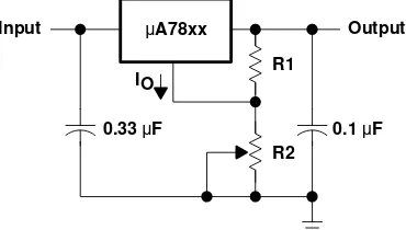
R1
0.33 µF
Input µA78xx Output
0.1 µF IO
R2
VO+Vxx)
ǒ
VR1xx)IQǓ
R2NOTE A: The following formula is used when Vxx is the nominal output voltage (output to common) of the fixed regulator:
Figure 3. Adjustable-Output Regulator
VO(Reg) R1
Input
IO IO = (VO/R1) + IO Bias Current
0.33 µF
µA78xx
Output
APPLICATION INFORMATION
µA7815C
0.1 µF 1N4001
0.1 µF
1N4001 0.33 µF
2 µF
1N4001 1N4001
VO = 15 V
VO = –15 V 20-V Input
–20-V Input µA7915C
[image:8.612.129.432.80.270.2]1 µF
Figure 5. Regulated Dual Supply
operation with a load common to a voltage of opposite polarity
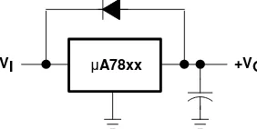
In many cases, a regulator powers a load that is not connected to ground but, instead, is connected to a voltage
source of opposite polarity (e.g., operational amplifiers, level-shifting circuits, etc.). In these cases, a clamp
diode should be connected to the regulator output as shown in Figure 6. This protects the regulator from output
polarity reversals during startup and short-circuit operation.
µA78xx +VO
+VI
–VO 1N4001
[image:8.612.192.395.383.454.2]or Equivalent
Figure 6. Output Polarity-Reversal-Protection Circuit
reverse-bias protection
Occasionally, the input voltage to the regulator can collapse faster than the output voltage. This can occur, for
example, when the input supply is crowbarred during an output overvoltage condition. If the output voltage is
greater than approximately 7 V, the emitter-base junction of the series-pass element (internal or external) could
break down and be damaged. To prevent this, a diode shunt can be used as shown in Figure 7.
µA78xx +VO
VI
[image:8.612.220.361.574.645.2]KTE (R-PSFM-G3)
PowerFLEX
PLASTIC FLANGE-MOUNT
0.360 (9,14) 0.350 (8,89)
0.080 (2,03) 0.070 (1,78)
0.010 (0,25) NOM 0.040 (1,02)
Seating Plane 0.050 (1,27)
0.001 (0,03) 0.005 (0,13)
0.010 (0,25) NOM
Gage Plane
0.010 (0,25)
0.031 (0,79) 0.041 (1,04)
4073375/F 12/00 NOM
3 1
0.350 (8,89) 0.220 (5,59) 0.360 (9,14)
0.295 (7,49) NOM
0.320 (8,13) 0.310 (7,87)
0.025 (0,63) 0.031 (0,79)
Thermal Tab (See Note C)
0.004 (0,10) M
0.010 (0,25) 0.100 (2,54)
3°– 6° 0.410 (10,41)
0.420 (10,67)
0.200 (5,08)
0.365 (9,27) 0.375 (9,52)
NOTES: A. All linear dimensions are in inches (millimeters). B. This drawing is subject to change without notice.
C. The center lead is in electrical contact with the thermal tab.
any product or service without notice. Customers should obtain the latest relevant information before placing orders and should verify that such information is current and complete. All products are sold subject to TI’s terms and conditions of sale supplied at the time of order acknowledgment.
TI warrants performance of its hardware products to the specifications applicable at the time of sale in accordance with TI’s standard warranty. Testing and other quality control techniques are used to the extent TI deems necessary to support this warranty. Except where mandated by government requirements, testing of all parameters of each product is not necessarily performed.
TI assumes no liability for applications assistance or customer product design. Customers are responsible for their products and applications using TI components. To minimize the risks associated with customer products and applications, customers should provide adequate design and operating safeguards.
TI does not warrant or represent that any license, either express or implied, is granted under any TI patent right, copyright, mask work right, or other TI intellectual property right relating to any combination, machine, or process in which TI products or services are used. Information published by TI regarding third-party products or services does not constitute a license from TI to use such products or services or a warranty or endorsement thereof. Use of such information may require a license from a third party under the patents or other intellectual property of the third party, or a license from TI under the patents or other intellectual property of TI.
Reproduction of information in TI data books or data sheets is permissible only if reproduction is without alteration and is accompanied by all associated warranties, conditions, limitations, and notices. Reproduction of this information with alteration is an unfair and deceptive business practice. TI is not responsible or liable for such altered documentation.
Resale of TI products or services with statements different from or beyond the parameters stated by TI for that product or service voids all express and any implied warranties for the associated TI product or service and is an unfair and deceptive business practice. TI is not responsible or liable for any such statements.
Following are URLs where you can obtain information on other Texas Instruments products and application solutions:
Products Applications
Amplifiers amplifier.ti.com Audio www.ti.com/audio Data Converters dataconverter.ti.com Automotive www.ti.com/automotive
DSP dsp.ti.com Broadband www.ti.com/broadband
Interface interface.ti.com Digital Control www.ti.com/digitalcontrol
Logic logic.ti.com Military www.ti.com/military
Power Mgmt power.ti.com Optical Networking www.ti.com/opticalnetwork
Microcontrollers microcontroller.ti.com Security www.ti.com/security
Telephony www.ti.com/telephony
Video & Imaging www.ti.com/video
Wireless www.ti.com/wireless
Mailing Address: Texas Instruments