Abstract—This Paper explains about GMSK modulation
implementation and simulation at SDR platform for the development of digital data communications base on SDR. GMSK modulation performance perceived at Packet Error Rate (PER) follow to GMSK modulation frequency variation, S/N ratio and also bit rate from delivered data. Beside that, this paper also explain about possibility of GMSK modulation by parallel processing for the development of furthermore SDR computing.
Index Terms—Gaussian minimum shift keying, packet error
rate, software-defined radio.
I.INTRODUCTION
long with the development of communication technology, Software-defined Radio (SDR) has become popular since it offers flexibility and re-configurability in encountering the rapid change of standard also the compatibility problems of standard varieties.
A
SDR is a wireless communication technology which function is determined by software, thus standard change of communication can be controlled easily, only by downloading software without changing the previous hardware.
SDR technology is suitable with the next generation of communication technology development which is still prioritizing on wireless and mobile communication. In the future, wireless communication system based on SDR will be required in the development of 3rd
generation cellular communication system, such as WCDMA and UMTS, and The Next Generation Networks (NGN) including The Rural Next Generation Networks (R-NGN).
This paper will describe the implementation of GMSK modulation for communicating of digital data on SDR platform and also as a part of the current research in building SDR platform which can be re-configured, including answering the research question of “How to design SDR platform which can be re-configured using commodity components.”
The rest of this paper is organized as follows. Section 2 discusses about SDR architecture along with SDR’s characteristics. Section 3 presents the GMSK modulation.
Section 4 shows BER Simulation for GMSK. Section 5 presents GMSK implementation and test result. Section 6 discusses the possibility parallel processing of GMSK. Finally, Section 7 is conclusion. Definition of mathematical symbols is presented in Appendix.
II.SDR ARCHITECTURE
Software-defined radio (SDR), sometimes shortened to software radio (SR), was introduced for the first time in 1991 by Joseph Mitola [1]. The word of SDR was used to show a radio class that could be re-configured or re-programmed [2], thus resulted a kind application of wireless communication with mode and frequency band determined by software function. Ideally, SDR offers flexibility, re-configurability, scalability and as multi mode as possible.
SDR architecture is developed based on conventional radio functions. The difference is all functions of signal processing on conventional radio are carried out fully by hardware while the functions of signal processing on SDR are carried out as much as possible by software. The major key in building SDR is the placement of ADC and DAC components as a divider between analog and digital domain, thus the signal processing can be carried out using software.
The ideal SDR architecture will place ADC/DAC as close as possible to the antenna, and will be followed by processor to carry out digital signal processing. The radio functions are carried out by the software which is operated by the current processor. Therefore, if there is standard change of communication, its change can be anticipated by upgrading the software [1][2]. However, the technology limitation and the expensive ADC/DAC wideband urge to change slightly SDR architecture in placing ADC/DAC. Therefore, a more realistic architecture would be as shown in Fig. 1.
The more realistic SDR architecture places ADC/DAC wideband after Down Converter/Up Converter, thus the conversion from analog to digital or its reverse is carried out on Intermediate Frequency (IF) signal which possesses lower frequency than RF signal. Today, that type of architecture are being developed widely and researched for the implementation. Fig. 1 shows the SDR architecture for both transmitter and receiver which can be represented using block
Simulation and Experimental Study of GMSK
Modulation on SDR Platform
Eko Marpanaji1 , Bambang Riyanto2, Armein Z.R. Langi2, Andri Mahendra2, Thay Liung2
Electrical Engineering STEI ITB, [email protected]
diagram as shown in Fig. 2.
Fig. 1. Realistic SDR Architecture
Software
Fig. 2. SDR Architecture for Transmitter and Receiver
Based on Fig. 2, the SDR platform performs transmitting and receiving functions. The transmitter (Tx) will perform some process such as base band signal processing, modulation, digital IF signal processing, and sending RF signal to the air. The receiver (Rx) will perform some process such as RF signal processing, channelization, digital IF signal processing, demodulation, and base band signal processing. As shown in Fig. 2, the computation process in the receiver will be more complex that in the transmitter.
ADC and DAC component will determine a point in which radio functions can be performed through a software. This point is usually called digital access point. The realistic SDR architecture will use software to process the digital IF signal. The major challenge in choosing ADC’s location is the problem of limited sampling frequency and economics factor. If the sampling frequency of Nyquist is hard to be done because of its digitalization IF signal is heavy, then the alternative is to apply under sampling toward IF signal, therefore it reduces the computation complexity from processor. The formula to determine under sampling frequency is as shown below:
the SDR system from figure 4, uses 20 MHz IF signal with 5 MHz bandwidth can be sampled with frequency of 22,5 MHz for m=1, or 17,5 MHz for m=2, or 11,66 MHz for m=3.
The next attention is on computation complexity which will determine the type and size of processor needed. The processor will implement the software of digital signal processing both for the receiver and transmitter. Besides to observe the functions generated by the software in determining computation complexity, the scalability factor for next development anticipation is also observed. All those steps will determine the processor’s size usually stated in term of Million Operations per Second (MOPS) or Million Instructions per Second (MIPS).
The biggest computation requirement is on the receiver side especially on filter part in channelization, which range from 100 to 200 operation/sample [2][4][5]. Using the sampling speed of 22.5 MHz results in 22.5 MSPS, thus it needs 2,250 up to 4,500 MIPS. Other computation requirements are modulation and demodulation process. As an illustration, modulation and demodulation FM require more or less 100 to 150 MIPS [6]. The total of these computation requirements will determine the type and the number of processor used in SDR platform. It means, for higher computation requirement which can not be carried out by a processor, the SDR architecture can use parallel computation architecture by involving several processors or implementing a part of signal processing function in form of FPGA.
Mitola (2000) gave the description of computation requirement for base-station in cellular communication system as following:
Refering to (2), the processing demand for each cell site is about 12,5 GOPS for IF processing section and 122,6 MOPS for base band signal processing. Illustrative processing demand is shown in Table I.
The biggest computation requirement in SDR system is on the receiver side especially channelization. Therefore, some researchers implemented channelization computation on receiver system in FPGA chip, and modulation process, demodulation, and base-band digital signal processing generated by another processor. By using FPGA, SDR performance can be significantly improved to pursue SDR flexibility toward higher RF frequency band.
power consumption, relative cost, computation ability. Other performance measure including Quality of Service (QoS), bit rate, bit error rate (BER), packet loss rate (PLR), packet error rate (PER), delay spread, and Grade of Service (GoS). Quantitative performance using QoS is typically stated as BER <10-3
, PLR < 10-2
, delay spread < 100 ms and GoS > 95% [2].
TABLE I. ILLUSTRATIVEPROCESSINGDEMAND (MITOLA, 2000)
*) Typically performed in digital hardware in contemporary implementations
Segmen Parameter Illustrative Value Demand
IF
122.6 MOPS per cell site
In the next section, the SDR implementation for digital communication using Gaussian Minimum Shift Keying (GMSK) modulation scheme along with the test result to observe its BER or PER will be discussed. Moreover, the modulator algorithm and GMSK demodulator to observe the possibility of implementing the process in parallel will be examined, so as to improve SDR performance.
III.GAUSSIAN MINIMUM SHIFT KEYING (GMSK)
The aim of this section is not to describe precisely the Gaussian Minimum Shift Keying (GMSK) modulation as it implies the presentation of too many mathematical concepts. Therefore, only brief aspects of the GMSK modulation are presented in this section. The GMSK modulation has been chosen as a compromise between spectrum efficiency, complexity and low spurious radiations (that reduce the possibilities of adjacent channel interference).
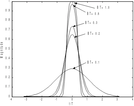
GMSK is derived from MSK which replace the rectangular pulse with a sinusoidal pulse and apply Gaussian filter for pulse-shaping. A Gaussian-shaped impulse response filter generates a signal with low side lobes and narrower main lobe than the rectangular pulse. Because this modulation used Gaussian filter for pulse-shaping then people calls this modulation as Gaussian Minimum Shift Keying (GMSK) modulation. The relationship between the pre-modulation filter bandwidth, B and the bit period, T defines the bandwidth of the system. GSM designers used a BT = 0.3 with a channel data rate of 270.8 kbps. This compromises between a bit error rate and an out-of-band interference since the narrow filter increases the inter-symbol interference and reduces the signal
power.
The response of Gaussian filter is determined by equation [7]:
Based on Equation (3), the filter response of Gaussian filter for several chosen values of BT is computed using MATLAB, and is plotted in Fig. 3
- 4 - 3 - 2 - 1 0 1 2 3 4
Fig. 3. Gaussian response filter with various of BT product
A.GMSK Modulator
Fig. 4 shows the principle of a GMSK modulator. The process occurred on modulator starts by changing bit stream
) (n
x with level 0 and one into bipolar stream bit x′(n)with level -1 and 1. Next, bipolar stream bit is processed by Gaussian filter possessing g(t) filter. This filter response is computed using convolution between bipolar bit streams
) (n
x′ and g(t). The result of convolution is then integrated in order to compute the phase ϕ(t). This phase will determine I-channel and Q-I-channel signals through equation:
(
())
Fig. 4. GMSK Modulator
in the following section.
B.GMSK Demodulator
The process occurred on GMSK demodulator in order to completely regain the information signal of bit stream is shown in Fig. 5. I-channel and Q-channel signals will be processed partly in case of its filtering and synchronization. The next process is partly phase computation for data rows exhibiting odd and even index numbers from the result of synchronization of I-channel and Q-channel signals to detect bit rows with previous level 0 and 1. Finally, the complete bit rows can be gained by joining both of bit rows, and therefore information signal of bit rows is regained according to what is sent by GMSK modulator. The detail algorithm of GMSK demodulator can be seen in [8].
Gaussian Filter
g(t)
Gaussian Filter I-Channel
Q-Channel
I-Channel Syncronization
Q-Channel Syncronization
Phase Calc. Data(odd)
Phase Calc. Data(even)
Combined bit
stream R1
R2.a
R2.b
R3.a
R3.b
R4.a
R4.b R5
Fig. 5. GMSK Demodulator
IV.BER SIMULATION
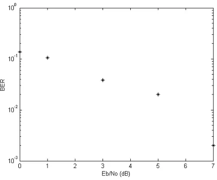
The Additive White Gaussian Noise (AWGN) channel can affect the signal transmitted, thus it causes miss-information. The difference message sent by message accepted on digital communication system is usually stated by bit error rate (BER). The effect of AWGN channel toward BER for modulation scheme can be simulated using MATLAB. The purpose of this simulation is to observe BER value gained from the change of signal quality or often sated as Eb/No numeral, where Eb = energy per bit and No = noise power. Fig. 6 shows the scheme configuration of GMSK modulation for simulating BER toward the change of Eb/No value.
GMSK Modulator
GMSK Demodulator
Gaussian Noise stream bit
input [0,1]
stream bit input [0,1]
BER Eb/No
Fig. 6. GMSK Configuration for BER Simulation
Fig. 7 shows the simulation result of GMSK modulation scheme stating connection between Eb/No toward the number of BER that can be gained. The conclusion obtained based on
simulation result for its several Eb/No value is that BER 3
10−
≤ if Eb/No≥ 5. Consequently, if the BER criteria that can be accepted is 10−3 then the comparison between Eb and No should be bigger or equal to 5.
Fig. 7. BER Simulation result for various Eb/No
V.IMPLEMENTATIONAND TEST RESULT
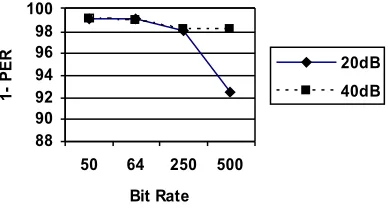
GMSK modulator and demodulator described previously is implemented in a USRP (Universal Software Radio peripheral) board that commonly used in SDR experiment from GNURadio. The Board is a front side of SDR system and has functions to execute digitalization function (ADC-DAC) and process filter channelization. The digital signal processing used personal computer with USB port as a link between USRP and PC. Operating system used Linux, with python programming language for level of application. The software used for digital signal processing was open source from GNURadio. This experiment would observe the performance of digital communication based on SDR using USRP board with GMSK modulation scheme. The transmission channel of coaxial cable RG58 was used to connect transmitter and receiver in order to anticipate AWGN channel also to limit output power from the smallest daughter-board basic TX. The experiment was carried out to observe Packet Error Rate (PER) stated by percentage of 1-PER or by the percentage of exactly accepted packet toward bit rate variation, S/N ratio, also carrier frequency (MHz). The result of observation is shown in Table II and Table III, the graphic observation is shown in Fig. 8 and Fig. 9.
smaller PER that would be resulted. From this observation, thus the smallest PER value or the biggest percentage of 1-PER that could be obtained by S/N ratio value of 20 dB and 40 dB for every bit rate variations.
TABLE II. BIT RATE VARIATIONAND S/N RATIOTO PER
(FREQ. 20 MHZ)
Bit rate S/N
(dB) N-Tx
N-Rcv
N-Loss
N-right
1-PER (N-right/
N-Tx)
bitrate: 500kb/sec spb: 2 decim: 64
0 667 3 664 0 0.00%
5 667 255 412 0 0.00%
10 667 569 98 0 0.00%
20 667 656 11 617 92.50%
40 667 656 11 655 98.20%
bitrate: 250kb/sec spb: 2 decim: 128
0 667 5 662 0 0.00%
5 667 251 416 0 0.00%
10 667 582 85 0 0.00%
20 667 656 11 654 98.05%
40 667 656 11 655 98.20%
bitrate: 64kb/sec spb: 4 decim: 250
0 667 2 665 0 0.00%
5 667 104 563 0 0.00%
10 667 510 157 0 0.00%
20 667 662 5 662 99.25%
40 667 661 6 661 99.10%
bitrate: 50kb/sec spb: 5 decim: 256
0 667 0 667 0 0.00%
5 667 113 554 0 0.00%
10 667 547 120 0 0.00%
20 667 663 4 662 99.25%
40 667 663 4 662 99.25%
Table III shows the observation result from the effect of carrier frequency on PER stated on percentage of 1-PER. In this experiment, constant values of 20 dB S/N ratio and 500 kbps bit rate were used. Fig. 9 shows the curve of observation result about GMSK modulation carrier frequency on PER stated in percentage of 1-PER by value S/N 20 dB and bit rate 500 kbps. Based on the curve, it could be stated that for the range of carrier frequency from 1 MHz to 30 MHz, the smallest PER (1-PER = 98.20%) was obtained on frequency of 15 MHz. Therefore, there was an optimum value of carrier frequency which result in smaller PER value.
88 90 92 94 96 98 100
50 64 250 500
Bit Rate
1
-
P
E
R 20dB
40dB
Fig. 8. The effect of bit rate on PER for S/N 20 dB and 40 dB
TABLE III. CARRIERFREQUENCYVARIATIONON PER
(S/N 20 DB DAN BIT RATE 500 KBPS)
Freq N-Tx N-Rcvd N-Loss N-Right 1-PER
(MHz) (N-Right /
N -Tx)
1 667 310 357 0 0.00%
3 667 656 11 651 97.60%
5 667 656 11 653 97.90%
15 667 656 11 655 98.20%
20 667 656 11 617 92.50%
25 667 656 11 640 95.95%
30 667 656 11 532 79.76%
0 20 40 60 80 100 120
1 3 5 15 20 25 30
Fre que ncy (M Hz)
1
-P
E
R
Fig. 9. Frequency influence to PER for S/N 20dB and Bit rate 500 kbps
VI.POSSIBILITY PARALLELPROCESSINGFOR GMSK
In parallel data processing task of DSP function divided into small tasks which were unconnected and independent for each of task. Next, those small tasks were executed concurrently and each of the result was re-joined in order to get the desired computation. The main purpose of parallel processing was to get maximum data throughput rate.
The thing that should be noticed in implementing sequential data processing to be parallel data processing is to do algorithm partition of digital signal processing where small tasks are created and it could be executed independently. A process could be divided into several processes separated each other if the data that would be processed was independent from another process. This partition result would be needed in determining time schedule from a computation task by controller processor.
In order to show the importance of FPGA, the partition of processing algorithm sequentially into parallel processing algorithm was carried out while using FPGA to replace DSP processor. There are only several algorithms that usually use on personal processor could be implemented directly in FPGA, because it could execute parallel signal processing process. Therefore, the previous sequential processing algorithm on personal processor should be changed into algorithm that could be implemented on parallel signal processing. Next, the partition of processing algorithm in parallel from GSK modulation and demodulation will be discussed.
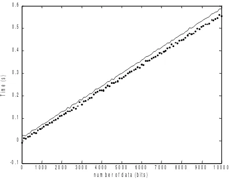
data resulted by previous process. Based on Fig. 4 for GMSK modulator and Fig. 5 for GMSK modulator, the sequence of signal processing process is stated by using the notation of 1, 2, 3, etc. While the processes notated by letter a, b, and c state the processes that could be carried out independently on the same time. T code states the process on modulator (T: transmitter), and R states the process on demodulator (R: Receiver).
The sequential process for modulator part were T1.a, T1.b, T2, T3, T4.a, and T4.b. T1.a and T1.b processes did not have data’s independent or in the other words; T1.b did not necessary to await process. Therefore, both of the processes could be carried out on the same time or in parallel. The parallel process also could be implemented on T4.a and T4.b since both of the processes could be carried out independently. Based on computation result between sequential process for all processes on modulator and several parallel processes, the necessary process time toward the number of data (bits) are shown on the following Fig. 8. The sequential process time is described by straight line (solid line), while process time implementing parallel process is shown by dots line. By implementing parallel process, modulator process time became slower that was 88.38%.
As for demodulator, the process’s sequence were R1, R2.a, R2.b, R3.a, R3.b, R4.a, R4.b and R5. Meanwhile, the processes of R2.a-R2.b, R3.a-R3.b, and R4.a-R.4b could be carried out separately and processed in parallel. The simulation result of process time toward the number variation of data’s bit for sequential and parallel process on demodulator are shown on Fig. 9. Solid line shows sequential process time, while dots line shows process time cy implementing parallel process. By implementing parallel process, thus process time was lower, that was 61.35%, and it was lower than sequential process.
0 1 0 0 0 2 0 0 0 3 0 0 0 4 0 0 0 5 0 0 0 6 0 0 0 7 0 0 0 8 0 0 0 9 0 0 0 1 0 0 0 0 - 0 . 1
0 0 . 1 0 . 2 0 . 3 0 . 4 0 . 5 0 . 6
n u m b e r o f d a t a ( b i t s )
T
im
e
(
s
)
Fig. 8. The difference of sequential and parallel processes time on GMSK modulator
Based on the simulation result, it seems that demodulator
part has significant difference compared to the parallel process. It happens because most processes happened on modulator were parallel processes. Therefore, the process on demodulator will be more efficient if it carries out in parallel. By implementing parallel process, the performance of modulator and demodulator can be more improved especially in pursuing the bit rate.
0 1 0 0 0 2 0 0 0 3 0 0 0 4 0 0 0 5 0 0 0 6 0 0 0 7 0 0 0 8 0 0 0 9 0 0 0 1 0 0 0 0 0
0 . 0 5 0 . 1 0 . 1 5 0 . 2 0 . 2 5
n u m b e r o f d a t a ( b i t s )
T
im
e
(
s
)
Fig. 9. The difference of sequential and parallel processes time on GMSK demodulator
VII.CONCLUSION
Based on the result of simulation study and GMSK modulation scheme experiment on the SDR platform, we conclude that:
1. To produce BER 3 10−
≤ , the signal quality transmitted should have Eb/No≥ 5.
2. The algorithm used for modulator and demodulator GMSK can be separated between the process that has higher dependency from the previous process and also has an independent process from the previous one. Hence, there is possibility to implement parallel computation for several processes which has no data dependency from previous process in GMSK.
3. The GMSK implementation on USRP as a SDR platform, for which channel is connected using coaxial cable, showed that PER is affected by S/N ratio, bit rate, and carrier frequency of GMSK modulator.
4. RF amplifier is needed to amplify the output signal resulted by USRP, such that BER and PLR value can be observed through AWGN channel
APPENDIX
bb
D = base-band signal processing requirement
bs
D = bit stream processing requirement
if
D = IF processing requirement
s
D = source processing requirement
o
D = overhead management processing
1
G = service isolation filter complexity
2
G = customer channel isolation complexity
3
G = bit steam process complexity per channel
d
G = demodulation process complexity
m
G = filter and modulation complexity N = the number of customer
b
R = the velocity of bit stream r = code velocity
a
W = service access bandwidth
c
W = bandwidth per channel
ACKNOWLEDGMENT
We would like to thank to the Dean of STEI ITB and the chief of PPTIK STEI ITB who have given opportunity and assistance in order to accomplish this research. This paper is a part of the current research about SDR platform development using ITB Research fund year 2006 based on contract No. 0018/K01.03.2/PL2.1.5/I/2006. We also thank to all people who contribute to this research.
REFERENCES
[1] J. H. Reed, Software Radio: A Modern Approach to Radio Engineering.
New Jersey: Prentice Hall, 2002.
[2] J. Mitola III, Software Radio Architecture. Object-Oriented Approaches
to Wireless Systems Engineering. Canada: John Eiley & Sons, Inc, 2000.
[3] M. E. Angoletta. (2003, Feb. 20). From Analog to Digital Domain.
[Online]. Available: http://humanresources.web.cern.ch/ humanre-sources/external/training/special/ DISP2003/DISP-2003_L01A_20Feb 03.pdf (20 Feb 2003).
[4] A. K. Salkintzis, H. Nie, P. T. Mathiooulos. (1999, August). ADC and
DSP Challenges in the Development of Software Radio Base Stations.
IEEE Personal Communications.
[5] C. H. Dick. (2001). Designand Implementation of High-Performance
FPGA Signal Processing Datapath for Software Define Radios. [Online]. Available: http:// www.eetasia.com/ARTICLES/2001AUG/ 2001AUG09_ ICD_AMD_RFD_ TAC01 .PDF.
[6] J. Huie, P. D’Antonio, R. Pelt. (2005). Synthesizing FPGA Cores for
Software-Defined Radio. [Online]. Available: http://www.altera.com/ cp/fpga-cores-for-sdr.pdf.
[7] S. Haykin, “Communication System,” 4th ed. New York: John Wiley &
Sons, Inc, pp. 396-402.
[8] H. Harada, R. Prasad, Simulation and Software Radio for Mobile