Ari Handono Ramelan
a, Pepen Arifin
b, Ewa Goldys
cSurface morphology, electrical and optical
properties n-type doped MOCVD grown GaSb
using dimethyltellurium
Dimethyltelluride has been used as a dopant source for GaSb epilayers grown via atmospheric pressure metal-organic chemical vapour deposition (MOCVD). It has been observed that the electron concentration (n) is proportional to the Te partial pressure in the vapour phase, untiln satu-rates at high Te partial pressure. Electron concentrations as high as 1.36·1018cm– 3have been measured with imper-fect morphology, and as high as 1.22·1018cm– 3with
ex-cellent, mirror like, morphology. These appear to be the highest electron concentrations reported to date for any MOCVD-growth epitaxial n-type GaSb doped with DMTe and grown at 5408C with a V/III ratio of 1.4. The absorp-tion spectra of GaSb doped with DMTe show that the heav-ily doped samples have a less abrupt edge. The absorption coefficient () strongly depends on the free carrier concen-tration. PL spectra of the epilayers are also reported.
Keywords:Te-doping; Gallium antimonide; MOCVD
1. Introduction
Antimony-based III-V semiconductors grown either lattice matched or slightly strained on GaSb substrates have re-ceived much attention both due to their potential applica-tions as optical devices in the wavelength of 1 – 4lm, and
for their potential use in tunnelling structures, exploiting the heterojunction offset. Although investigations in laser diodes have been carried out by many groups [1 – 4] prob-lems still remain with the growth of device-quality GaSb layers [5], most significantly with doping.
Undoped GaSb usually exhibits p-type conductivity, ow-ing to native lattice defects includow-ing Sb vacancies, antisite defects i. e., Ga atoms on Sb site, VGaGaSb[6]. The group-VI elements such as S, Se, and Te are commonly used as n-type dopants in GaSb because the group-VI elements such as Si and Sn are amphoteric and lead to heavily com-pensated p-type layers [7]. Researchers have investigated the n-type doping of GaSb by all major techniques [8 – 12]. In the course of this work, it was identified that group-VI elements have high vapour pressure and segregation coeffi-cient, making it difficult to control the electron concentra-tion. Therefore, the growth of GaSb doped with Te is still a challenge and worth in-depth exploration.
In this work, dimethyltelluride (DMTe) has been used as a dopant for the MOCVD growth of GaSb. The physical properties of MOCVD grown Te-doped GaSb on semi insu-lating (SI) GaAs substrates are reported. The effects of dop-ant flow rate on surface morphology, electrical and optical properties have been determined.
2. Experimental procedure
2.1. Growth condition
Growth was carried out in a horizontal quartz atmospheric pressure MOCVD reactor. Six IR lamps were used to heat the graphite susceptor. TMGa (trimethylgallium) and TMSb (trimethylantimony) were used as metalorganic sources and kept at a constant bath temperature of – 9 and 08C, respectively, which correspond to a molar flow of 2.53 and 1.82lmol min– 1respectively, for 1 sccm
hydro-gen flows through the metalorganics. DMTe (dimethyltel-lurium) was used as dopant precursor and kept at a constant temperature of 278C. High purity H2was passed through a
proprietary metal hydride filter made by Ultra Pure Sys-tems. In this work, we have used a group V mole fraction, XTMSb= 10.1·10– 5, an input V/III = 1.4, a DMTe mole
fraction,XDMTe= 1.42·10– 6– 7.08·10– 6, a growth
tem-perature of 5408C and the total flow rate was 8 l · min– 1. Values of DMTe flow with corresponding mole fractions of DMTe in the input gas stream for various samples are given in Table 1. Substrates used were SI-GaAs(100) from Freiberger (Germany). Prior to the growth, substrates were immersed for 5 min in each of trichloroethylene at a tem-perature of 1008C, acetone and methanol and then etched in H2SO4: H2O2: H2O = 1 : 1 : 8 solution for 30 s followed
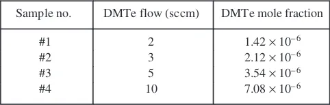
Table 1. Values of DMTe flows with corresponding mole frac-tions of DMTe for n-type GaSb growth.
Sample no. DMTe flow (sccm) DMTe mole fraction
#1 2 1.42·10– 6
#2 3 2.12·10– 6
#3 5 3.54·10– 6
#4 10 7.08·10– 6
aFaculty of Mathematics and Natural Sciences Sebelas Maret University (UNS), Physics Department, Surakarta, Indonesia bFaculty of Mathematics and Natural Sciences Bandung Institute of Technology (ITB), Physics Department, Bandung,
Indonesia
cFaculty of Science and Engineering, Macquarie University, Physics Department, Sydney, Australia
W
2011
Car
lHanse
r
Verlag,
M
u
nich,
G
e
r
man
yw
ww.
ijm
r.
de
N
o
t
fo
ru
s
ei
ni
n
t
e
r
ne
t
o
r
in
tr
ane
ts
i
t
e
s.
N
o
t
fo
r
elec
tr
onic
di
str
ib
ut
ion
by a DI (deionised water) water rinse. The substrate were then blown dry by N2, before being loaded into the reactor.
2.2. Characterisation
Van der Pauw Hall measurements were performed in the temperature range of 300 – 10 K on the 3lm thick epilayers
grown on the SI-GaAs substrates. The absorption of Te-doped GaSb samples was measured using a UV-Vis-NIR Spectrophotometer. Photographs of sample morphology were taken using a Nomarski phase contrast microscope. Photoluminescence (PL) was measured at a temperature of 100 K using a cryogenic system. The PL spectra were de-tected using an InGaAs photodetector. A diode laser, emit-ting photons at 950 nm, used for excitation.
3. Results and discussion
3.1. Surface morphology
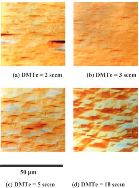
The morphology obtained from samples grown using di-methyltellurium (DMTe) as a dopant is illustrated in Fig. 1. The epilayers shown in Fig. 1a – d were grown with the DMTe flow rate in the range of 2 – 10 sccm for a growth temperature of 5408C. Some degradation of morphology can be seen for the samples grown with a 5 and 10 sccm DMTe flow, where hillocks and ripples are typically ob-served. The sample grown with 10 sccm DMTe shows pyr-amid-like hillocks about 10lm across. This may be due to
Te precipitation. Similar results reported for Te-doped GaAs using diethyltelluride (DETe) in low pressure
orga-nometallic vapour phase epitaxy (LPOMVPE) [13, 14] show that the degradation of morphology occurs at the highest electron concentrations. Figure 1a shows the sur-face morphology for the GaSb sample doped with 2 sccm DMTe. The surface is mirror like and fewer hillocks occur. The sample shown in Fig. 1b was grown at 3 sccm and the surface morphology is mirror-like.
3.2. Electrical properties
Table 2 shows the electrical properties obtained from Hall measurements of 3lm-thick GaSb layers doped with Te.
Hall concentrations from 3:541017cm3 to 1:36 1018cm3were obtained by varying the DMTe source
va-pour pressure. It should be noted here that the measured Hall concentration, particularly at room-temperature, is not considered to be the total free-carrier concentration. It was observed that electron concentration nis proportional to Te partial pressure in the vapour phase until it saturates at high Te partial pressure. Measured electron concentra-tions were as high as 1:361018cm3with imperfect mor-phology and as high as 1:221018cm3 with excellent, mirror like, morphology. These appear to be the highest electron concentrations reported to date for any epitaxial n-type GaSb. The electron concentration shows a linear de-pendence on XDMTe and saturates near n= 1.36·
1018cm– 3whenX
DMTe> 3.5·10– 6as shown by the circles
in Fig. 2. A possible explanation for this behaviour is that Te incorporation results from a competition between Sb and Te atoms for Sb free-site occupation [15]. The squares in Fig. 2 show the results obtained by Wang et al. [16] using a DETe dopant MOCVD growth at a growth temperature of 5508C, and with V/III = 1.8. The higher mole fraction of DMTe in the saturation region is presumably caused by the higher vapour pressure of DMTe compared with DETe. Similar results were reported by Ehsani et al. [17] for the growth of InGaSb with DETe doping, the electron concen-tration was found to increase linearly as the DETe increas-ed, reaching a saturated concentration of 1.5·1018cm– 3.
When the DETe mole fraction was increased further, the electron concentration decreased.
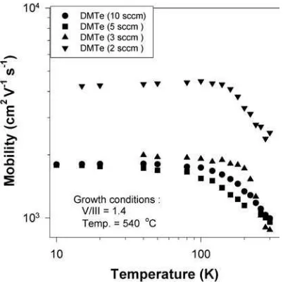
Temperature-dependent Hall mobilities for four GaSb layers are shown in Fig. 3. Meanwhile the electron concen-tration is displayed in Fig. 4. The mobility for a low-doped GaSb layer with nH = 3.54 · 1 017 cm– 3 (2 sccm DMTe
flow) at 300 K is 2 543 cm2V1s1 and peaks at about
100 K with a value of 4 478 cm2V1s1. Below this
temperature, the mobility drops due to ionised impurity scattering, the dominating scattering mechanism at low temperatures. A similar behaviour was observed for the sample grown with 3 sccm DMTe flow where the donor concentration was equal to nH = 1.22 · 1018cm– 3. For a more highly-doped GaSb layernH= 1.36·1018cm– 3, the
mobility does not show a peak and remains relatively con-stant with decreasing temperature. A considerably lower mobility was observed for GaSb layers when the sample was doped with Te higher than the saturation level.
3.3. Optical properties 3.3.1. Absorption spectra
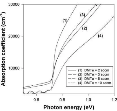
The absorption spectra at 300 K for the four samples with different DMTe concentration of
Fig. 1. Nomarski photograph of Te doped n-GaSb grown on SI-GaAs: (a) 2 sccm; (b) 3 sccm; (3) 5 sccm; (4) 10 sccm.
W
2011
Car
lH
an
s
e
r
Ve
r
lag,
Mu
nich,
G
e
r
man
yw
ww.
ijm
r.
de
N
o
t
fo
ru
s
ei
ni
n
t
e
r
ne
t
o
r
in
tr
ane
ts
i
t
e
s.
N
o
t
fo
r
elec
tr
onic
di
str
ib
ut
ion
1 2 sccm, 2. 3 sccm, 3. 5 sccm, and 4. 10 sccm,
respectively, are shown in Fig. 5. The most heavily doped sample showed a less abrupt absorption edge. The absorption coefficientstrongly depends on the free carrier concentra-tion. The absorption spectra (1) of the GaSb sample is shifted towards lower energies due to the effective bad gap shrink-age resulting from the merger of the acceptor band and
va-lence band [18, 19]. However, the energy shift for band edge absorption for the GaSb with low concentration of DMTe is very small due to low hole concentration. In constrast, the spectra (2), (3) and (4) for the Te-doped n-type GaSb sam-ples are shifted towards higher energies with increasing elec-tron concentration. This shift, known as the Burstein – Moss shift [20], is due to the filling of the conduction band and has been reported in many heavily doped n-type materials such as InP [21], GaAs [22], and GaSb [23]. With the small effective electron mass for GaSb ðme0:014moÞ [2], the lower density of states at the bottom of the conduction band may result in a degenerate n-type material, even at electron concentrations as low as 81015cm3[24].
3.3.2. Photoluminescence (PL) spectra
The PL spectra of Te-doped n-GaSb samples grown at 5408C and V/III = 1.4 with various concentrations of DMTe are shown in Fig. 6. All PL spectra of the highly doped samples (n 1017cm3) consist of a single peak, i. e. emission band which is attributed to a free-to-bound (or donor-to-acceptor pair) recombination involving an ac-ceptor level at about 82 meV, as reported by Bignazzi et al. [25]. Only conjectures can be proposed concerning its origin; a complex defect consisting of a Te donor and a stoi-chiometric defect seems the most reasonable choice [24, 26]. As the doping level increases typical emission doping effects appear. The acceptor related band becomes less well resolved and the band broadens.
The PL spectra of heavily doped samples are charac-terised by a broadening and blue shift of the PL bands when Table 2. Hall measurements on Te-doped GaSb layers as a function of DMTe vapour pressure.
DMTe flow rate (sccm)
nH(300 K)
(cm– 3)
lH(300 K)
(cm2· V– 1· s– 1)
nH(77 K)
(cm– 3)
lH(77 K)
(cm2· V– 1· s– 1)
2 3.54·1017 2 543 5.4
·1017 4 478
3 1.22·1018 877 1.4
·1018 1 891
5 1.36·1018 956 1.5
·1018 1 730
10 1.00·1018 997 1.3
·1018 1 755
Fig. 2. Electron concentration dependence on Te mole fraction.
Fig. 3. Mobility of Te doped n-GaSb with different DMTe flows as a function of temperature.
Fig. 4. Carrier concentration of Te doped n-GaSb with different DMTe flow as a function of temperature.
W
2011
Car
lH
an
s
e
r
Ve
r
lag,
Mu
nich,
G
e
r
man
yw
ww.
ijm
r.
de
N
o
t
fo
ru
s
ei
ni
n
t
e
r
ne
t
o
r
in
tr
ane
ts
i
t
e
s.
N
o
t
fo
r
elec
tr
onic
di
str
ib
ut
ion
the free carrier concentration increases as depicted in Fig. 6. These features can be explained by considering the interplay of different effects connected with heavy doping: (i) conduction-band filling,
(ii) bandgap narrowing due to carrier – carrier and carrier – impurity interactions and
(iii) formation of band tails due to doping inhomogeneities [27, 28].
4. Conclusions
n-type GaSb has been grown using MOCVD with DMTe as a dopant in the range of 2 and 10 sccm. It has been observed that the electron concentration (n) is proportional to the Te partial pressure in the vapour phase, untilnsaturates at high Te partial pressure. Electron concentrations as high as 1.36·1018cm– 3have been measured with imperfect
mor-phology, and as high as 1.22·1018cm– 3 with excellent, mirror like, morphology. These appear to be the highest electron concentrations reported to date for any MOCVD-growth epitaxial n-type GaSb doped with DMTe and grown at 5408C with a V/III ratio of 1.4.
The absorption spectra of GaSb doped with DMTe show that the heavily doped samples have a less abrupt edge. The absorption coefficientstrongly depends on the free carrier concentration. The absorption spectra of the GaSb sample shift towards lower energies due to the effective band gap shrinkage resulting from the merger of the accep-tor band and valence band. The departure from the known band gap of GaSb is very small due to low hole concentra-tion. However, in the spectra of n-type GaSb samples doped with DMTe using flows of 3, 5 and 10 sccm, the absorption edge shifts towards higher energies with increasing electron concentration. This is due to the Burstein – Moss effect.
All PL spectra of the highly doped samples (n 1017cm3) consist of single peak, i. e. emission band which
is attributed to a free-to-bound (or donor-to-acceptor pair) recombination involving an acceptor level at about 82 meV. The PL spectra of heavily doped samples are char-acterised by a broadening and blue shift of the PL bands with increasing free carrier concentration.
The financial support from the Directorate General of Higher Educa-tion (DIKTI) the Ministry of NaEduca-tional EducaEduca-tion (KEMENDIKNAS) the Government of Indonesia Republic is gratefully acknowledged.
References
[1] R.J. Menna, D.R. Capewell, R.U. Matinelli, P.K. York, R.E. En-stron: Appl. Phys. Lett. 59 (1991) 2127. DOI:10.1063/1.106101 [2] H. Toyota, T. Yasuda, T. Endoh, S. Nakamura, Y. Jinbo, N.
Uchi-tomi: J. Crystal Growth. 311 (2009) 802. DOI:10.1016/j.jcrysgro.2008.09.063
[3] H.K. Choi, S.J. Egflas: IEEE J. Quantum Electron. QE-27 (1991) 1555. DOI:10.1109/3.89977
[4] P. Gladkov, E. Monova, J. Weber: Semicond. Sci. Technol. 12 (1997) 1409. DOI:10.1088/0268-1242/12/11/013
[5] A. Sasaki, A. Ohishi, E. Sogawa, Y. Takeda, S. Fujita in: Gallium Arsenide and Related Compounds, Institute Physics Conference (1982) 83.
[6] C. Anayama, T. Tanahashi, H. Kuwatsuka, S. Nishiyama, S. Iso-zumi, K. Nakajima: Appl. Phys. Lett. 56 (1990) 239.
DOI:10.1063/1.102842
[7] K.F. Longenbach, S. Xin, W.I. Wang: J. Appl. Phys. 69 (1991) 3393. DOI:10.1063/1.348518
[8] I. Poole, M.E. Lee, K.E. Singer, J.E.F. Frost, T.M. Kerr, C.E.C. Wood, D.A. Andrew, W.J.M. Rothwell, G.J. Davies: J. App. Phys. 63 (1988) 395. DOI:10.1063/1.340251
[9] F. Pascal, F. Delannoy, J. Bougnot, L. Gouskov, G. Bougnout, P. Grosse, J. Kaoukab: J. Electron. Mater. 19 (1990) 1987. DOI:10.1007/BF02651744
[10] T.H. Chiu, J.A. Ditzenberger, H.S. Luftman, W.T. Tsang, N.T. Ga: Appl. Phys. Lett. 56 (1990) 1688. DOI:10.1063/1.103118 [11] J.F. Chen, A.Y. Chao: J. Appl. Phys. 70 (1991) 277.
DOI:10.1063/1.350296
[12] F. Nakamura, K. Tiara, K. Funato, H. Kawai: J. Crystal Growth 115 (1991) 474. DOI:10.1016/0022-0248(91)90789-8
[13] Y.H. Houng, T.S. Low: J. Crystal Growth 77 (1986) 278. DOI:10.1016/0022-0248(86)90311-8
[14] S.Z. Sun, E.A. Armour, K. Zheng, C.F. Schaus: J. Crystral Growth 113 (1991) 103. DOI:10.1016/0022-0248(91)90014-V
[15] C.A. Wang, K.F. Jensen, A.C. Jones, H.K. Choi: Appl. Phys. Lett. 68 (1996) 400. DOI:10.1063/1.116698
[16] H. Gotoh, K. Sasamoto, S. Kuroda, T. Yamamoto, K. Kitamura, M. Fukushima, M. Kimata: Jpn. J. Appl. Phys. 20 (1981) 893. DOI:10.1143/JJAP.20.L893
[17] H. Ehsani, I. Bhat, C. Hitchcock, R.J. Gutmann, G. Charache, M. Freeman: J. Crystal Growth 195 (1998) 385.
DOI:10.1016/S0022-0248(98)00710-6 Fig. 5. Optical absorption spectra of four GaSb samples with different
concentration of DMTe at 300 K.
Fig. 6. PL spectra of GaSb doped with different concentrations of DMTe.
W
2011
Car
lH
an
s
e
r
Ve
r
lag,
Mu
nich,
G
e
r
man
yw
ww.
ijm
r.
de
N
o
t
fo
ru
s
ei
ni
n
t
e
r
ne
t
o
r
in
tr
ane
ts
i
t
e
s.
N
o
t
fo
r
elec
tr
onic
di
str
ib
ut
ion
[18] N.A Yakusheva, V.G. Pogadaev: Crystal Res. Technol. 27 (1992) 21. DOI:10.1002/crat.2170270104
[19] D.W. Kisker, M.L. Steigerwald, T.Y. Kometani, K.S. Jeffers: Appl. Phys. Lett. 50 (1987) 23. DOI:10.1063/1.97766
[20] E. Burstein: Phys. Rev. 83 (1954) 632. DOI:10.1103/PhysRev.93.632
[21] M. Bugajski, W. Lewandoski: J. Appl. Phys. 57 (1985) 521. DOI:10.1063/1.334786
[22] M.C. Wu, Y.K. Su, K.Y. Cheng, C.Y. Chang: Solid State Elec-tron. 31 (1988) 251. DOI:10.1016/0038-1101(88)90137-2 [23] E.I. Chaikina, Sh. Egemberdieva, A.S. Filipchenko: Phys. Status
Solidi A 84 (1984) 541. DOI:10.1002/pssa.2210840225 [24] M.C. Wu, C.C. Chen: J. Appl. Phys. 73 (1993) 8495.
DOI:10.1063/1.354085
[25] A. Bignazzi, A. Bosacchi, R. Magnanini: J. Appl. Phys. 81 (1997) 7540. DOI:10.1063/1.365297
[26] A.I. Labedev, I.A. Strelnikova: Sov. Phys. Semicond. 13 (1979) 299.
[27] A. Haufe, R. Schwabe, H. Fiesele, M. Ilegems: J. Phys. C: Solid State Phys. 21 (1988) 2951. DOI:10.1088/0022-3719/21/15/026 [28] G. Borghs, K. Bhattacharya, K. Deneffe, P. Van Mieghem, R.
Mertens: J. Appl. Phys. 66 (1989) 4381. DOI:10.1063/1.343958
(Received August 22, 2010; accepted August 31, 2011)
Bibliography
DOI 10.3139/146.110597
Int. J. Mat. Res. (formerly Z. Metallkd.) 102 (2011) 11; page 1403 – 1407 #Carl Hanser Verlag GmbH & Co. KG ISSN 1862-5282
Correspondence address
Dr. Ari Handono Ramelan
Physics Department, Faculty of Mathematics and Natural Sciences Sebelas Maret University (UNS)
Jl. Ir. Sutami No. 36A Surakarta 57126 Indonesia
Tel.: +62 271 663 375 Fax: +62 271 663 375
E-mail: aramelan@mipa.uns.ac.id; aramelan_uns@yahoo.com
You will find the article and additional material by enter-ing the document number MK110597 on our website at
www.ijmr.de
W
2011
Car
lH
an
s
e
r
Ve
r
lag,
Mu
nich,
G
e
r
man
yw
ww.
ijm
r.
de
N
o
t
fo
ru
s
ei
ni
n
t
e
r
ne
t
o
r
in
tr
ane
ts
i
t
e
s.
N
o
t
fo
r
elec
tr
onic
di
str
ib
ut
ion