Reduction of Total Harmonic Distortion (THD) on Multilevel
Inverter with Modified PWM using Genetic Algorithm
Lucky Pradigta S.R., Ony Asrarul Q., Zainal Arief, Novie Ayub Windarko Politeknik Elektronika Negeri Surabaya
Kampus PENS, Jl. Raya ITS, Sukolilo, Surabaya 60111, Indonesia [email protected]; [email protected]; [email protected]; [email protected]
Abstract
In this research, modified PWM has been applied to the multilevel inverter (MLI) single‐phase three‐level diode clamp full bridge. Modified PWM is performed to produce minimum Total Harmonic Distortion (THD) the voltage because the quality of the good voltage is indicated by small THD. The THD indicates the quality of AC voltage source. The THD standard by the IEEE STD 519‐1992 Harmonic Voltage Limits is 5% and the Pacific Corp standard is 8%, if the THD value is greater than the THD standard it can cause the electronic load to be damaged due to the damaged waveform. Modified PWM is applied by adding a 50 Hz sinusoidal reference signal with a sinusoidal signal which has a certain amplitude, frequency and phase shift angle. The frequency of the adder signal is the frequency at which the value of the individual harmonic voltage appears (n harmonic). To get maximum result, optimization using Genetic Algorithm (GA) method to determinate amplitude & phase shift angle done. The result of implementation hardware with modified PWM shows smaller THD voltage compared to the THD voltage with Sinusoidal Pulse Width Modulation (SPWM) switching up to 0.19 or decrease 65,51 % for modified PWM of harmonic injection n = 7 with GA optimization ma= 0.8 (A=0.0936 and ø = 0 rad) and up to 0.08 or decrease 12,30 % for modified PWM of harmonic injection n = 22 with GA optimization ma = 0.4 (A=0.1221 and ø = 0 rad).
Keywords: Multilevel Inverter, Modified PWM, Genetic Algorithm.
1. INTRODUCTION
The increasing need for electrical energy sources encourages people to use renewable electricity. The most popular renewable energy is photovoltaic. Photovoltaic is a component that utilizes sunlight to produce voltage. The resulting voltage of a photovoltaic is a DC voltage. DC voltage cannot be directly used because the existing electrical system is dominated by the electric load with AC voltage source. Thus, it requires a tool to convert DC voltage into AC voltage.
Inverter is a device used to convert DC voltage into AC voltage that utilizes the switching conditions of a switch component to produce AC voltage. The output voltage of the inverter still has a low voltage quality that is indicated by a very large Total Harmonic Distortion (THD). This voltage requires a filter to produce the output voltage with minimum THD voltage so as to generate a suitable sinusoidal wave for the voltage source [12]. THD is a measurement of the quality of voltage or current. In normal conditions the output voltage form is a sinusoidal wave where THD is close to or equal to 0 (zero). THD is the percentage value between the total components of harmonics with its fundamental components. The greater the percentage of THD, the greater the risk of equipment damage. In accordance with the standards by IEEE STD 519‐1992, the standard Harmonic Voltage Limits on the general system is 5% [27], and 8% is for Pacific Corp standard [28]. If the THD value is greater than the THD standard, it can lead to the destruction of electrical equipment, the burning of cable/conductor, overheat on the electric motor, and error on the electromechanical measurement of KWH meter.
To overcome this, the multilevel inverter was built to improve the output voltage quality of the conversion. Multilevel inverter output has better voltage quality than inverter [2][3][7]. The voltage quality is indicated by smaller THD. This is because multilevel inverters emit voltage wave on stages according to a level that resembles a sinusoidal form. One type of multilevel inverter is a multilevel inverter clamp diode [16]. This type would be used for the conversion tool from DC voltage to AC voltage.
The output voltage form of the multilevel inverter depends on the switching method used. Much research has been done on the topic of the switching method [1][9][14][17][19]. Shared methods were tested including Pulse Width Modulation (PWM), Sinusoidal Pulse Width Modulation (SPWM) and Third Harmonic Pulse Width Modulation (THIPWM) to produce voltage with minimum THD voltage. With the results presented in various papers and journals [4][5][12][21], the researchers tried to research the switching method used in multilevel inverters to obtain a minimum or very small THD
voltage. In this study, the researchers have made modified PWM for multilevel
2. RELATED WORKS
In a study by Ahmet M. Hava [1] with the title of A High Performance
Generalized Discontinuous PWM Algorithm has been produced
Discontinuous PWM algorithm that was tested on inverter three‐phase as voltage source of motor. Discontinuous PWM test algorithm is performed in a laboratory under constant stress and frequency (constant) conditions on an induction motor with a capacity of 5 Hp 460 V 21 A. The dc voltage source used is 620 V. The frequency of the signal the keeper is 5 KHz. DSP was used in computing to compare the reference signal with the seeker signal. The Generalized Discontinuous PWM Algorithm (GDPWM) is generated from computing by applying the Switching Loss Function (SLF) algorithm
(Ѱ = + ≤ ). In this study, the researcher compared various
methods of PWM to produce Harmonic Distortion Factor or known as the minimum Total Harmonic Distortion. From the results of this study, it was obtained the best sequence of the type of Discontinuous PWM DPW M 3, DPW M 1, DPW M2, THIPW M 1/4, THIPWM 1/6; SVPWM, and SPWM. Using DGWM could lower harmonic distortion and losses on switching.
In a study by Xiaoming Yuan [26] with the title of Fundamentals of a New Diode clamping Multilevel Inverter has generated multilevel inverter topology with clamp diode type. Multilevel inverter on diode clamping type is designed for five‐levels with one leg. Tests in this study were conducted on a laboratory scale with prototype generation of five‐level clamping diode inverters with half bridges with 120 V DC voltage sources. In the test used inductor load of 8 mH connected in series with a resistor of 12 Ω that is connected between the outputs of the inverter with a neutral point. In the
inverter modulation the harmonics of the 5th and 7th harmonics were
performed and implemented. The research resulted that inverter with diode clamp type would help to form the level of inverter output voltage. In addition, the diode clamp type would reduce the unequal voltage between the voltage sources that were divided into the formation of the voltage level in the output inverter.
In a study by Olorunfemi Ojo [19] with the title of The Generalized Discontinuous PWM Scheme for Three Phase Voltage Source Inverter has generated signal modulation used for carrier signals on sinusoidal reference signals. Discontinue PWM was modulated to two‐level on three‐phase voltage generating inverters or so called Voltage Source Inverter (VSI). Modulation is generated by the inverter under balanced or unequal phase voltage conditions. In this research generation Generalized Discontinuous PWM was done by computing. The modulation function was generated by comparing high‐frequency triangular (carrier) waves ranging from ‐1 to 1 with reference modulation waves. The Generalized Discontinuous PWM was
indicated with = 0.5 1 − 2 ) − + − 1); with
In a study by Said Barkati [22] with the title of Harmonic Elimination in Diode Clamped Multilevel Inverter Using Evolutionary Algorithms generated comparison of results for harmonic optimization. The result was that the harmonic of multilevel inverter out was with a minimum value. The optimized method used was Genetic Algorithm (GA) and Particle Swarm that was applied for switching angle computing on three‐phase seven‐level inverter. In the optimization process using GA, the researchers did the optimization at the angle of the shift done on the reference signal that
was ,, ., . GA parameters used were Population = 100, Generation = 100,
Crossover Probability = 0.33 and Mutation Probability = 0.33. It was observed that the maximum modulation (m) at 1.07. Parameter Particle Swarm run for 20 particles with w = 0.75, p_incr = 1.8 and g_incr = 1.8.
In a study by Reza Salehi [21] with the title Elimination of Low Order Harmonics in Multilevel Inverter Using Genetic Algorithm has been produced the process of eliminating harmonics with Selective Harmonic Elimination Pulse Width Modulation (SHEPWM) applied to multilevel inverter with cascade type of inverter with nine‐level. SHEPWM was done using the Genetic Algorithm (GA) optimization method. GA was implemented on nine‐ level inverter for harmonic elimination of 5, 7, and 11. For fitness values less than or equal to 10‐2, it was expected to eliminate harmonics. Ms expected (feasible) can be seen on M = 0.34 [0.44‐0.47], 0.51 [0.54‐0.6], 0.63 [0.67‐ 0.69], [0.73‐0.85] and 0.92.
3. ORIGINALITY
In this study, the research originality is modified PWM of the reference signal by adding a certain signal as well as doing the GA optimization on amplitude and phase shift angle value of the adder signal. GA optimization
process was done with Matlab and PSIM simulation Off‐line. After obtaining
4. SYSTEM DESIGN
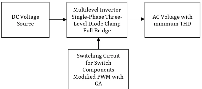
Figure 1 shows the block diagram of the system reducing the THD output voltage of the multilevel inverter.
Figure 1. System Block Diagram
4.1 Multilevel Inverter
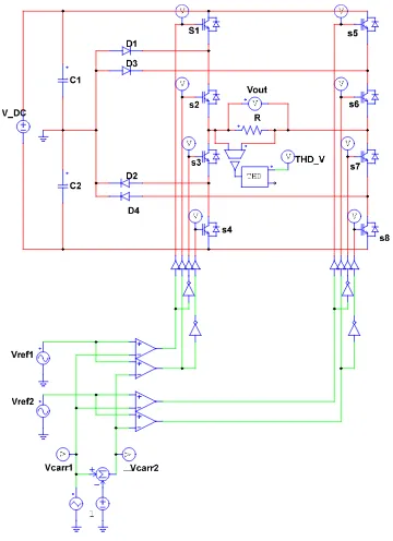
Multilevel inverter design is multilevel inverter single‐phase three‐level diode clamp full bridge according to the circuit in figure 2. The switching
component used IRFP460 MOSFET. The voltage drive Vgs MOSFET was
between 10 to 20 Volt dc. The IRFP460 MOSFET was used with current
capacity = 20 Ampere with voltage Vds = 600 Volt dc. For the diode clamp,
fast recovery diode with type R30120G2 was used. The fast recovery diode type was chosen because it adjusts to the magnitude of switching from the dc voltage entering the switching component, where the switching frequency for the carrier signal was 1 KHz. To provide Vdc/2 for multilevel inverter source, 220 uF capacitor mounted in series was used.
Figure 2. Multilevel Inverter Single‐Phase Three‐Level Diode Clamp Full Bridge DC Voltage
Source
Multilevel Inverter Single‐Phase Three‐ Level Diode Clamp
Full Bridge
AC Voltage with minimum THD
Switching Circuit for Switch Components Modified PWM with
In multilevel inverters with diode clamp type, basically, the voltage of the clamping diode is used. The DC voltage source was divided into parts depending on the level, while the capacitor in pairs in series with a neutral point was between the capacitor in the middle. To know the parameters of multilevel inverter design with clamp diode type, observe the following:
/0 12 3% %45467 = − 1) (1)
m is level for multilevel inverter
Vdc is DC Voltage Source
Va is Output Voltage Multilevel Inverter
The switching component condition in leg 2 was equal to leg 1 but there was an angular difference from the reference signal that was a sinusoidal signal of ‐120ᵒ. For Switch 3, it was complementary from Switch 1 while for Switch 4, it was complementary of Switch 2. Switch 1 and Switch2 were the reverses. In table 1 will be shown ON/OFF switching process for Multilevel Inverter Single‐Phase Three‐Level Diode Clamp for 1 leg.
Table 1.
4.2 Switching Sinusoidal Pulse Width Modulation
The formation of the output voltage of the multilevel inverter depends on the switch components used by each leg. One of the switching methods of multilevel inverter is the method of Switching Sinusoidal Pulse With Modulation (SPWM). This method compares the sinusoidal signal (A Sin ωt) as a reference signal with a triangle signal as a carrier wave. The carrier
wave frequency must be greater than the frequency of the sinusoidal wave (fc
important parameters namely amplitude and frequency modulation, which is
denoted by ma and mf. Amplitude modulation index (ma) is the ratio
between the amplitude voltage reference signal 2 )and the amplitude
voltage carrier signal 64 72 ).
= ?@AB
?CD@@EA@ (6)
While the frequency modulation index (mf) is the ratio between the
frequency carrier signal F GG HG) and the frequency reference signal GHI).
I =ICD@@EA@I
@AB (7)
The switching condition ON/OFF was obtained by comparing sinusoidal signals with triangular stratified signals. The sinusoidal amplitude was 1 so as to have peak to peak = 2. As for the amplitude of triangular‐level signal, the first level was ‐1 to 0 and the second level was 0 to 1. The frequency of the sinusoidal reference signal was 50 Hz and the frequency of the carrier signal was 1 KHz. In switching, microcontroller STM32F407 was used to generate signal switching to MOSFET. The signal was processed on microcontroller using signal generator function so that output from the microcontroller in the form of digital was in form of output condition of ON and OFF.
4.3 Switching Modified Pulse Width Modulation
Modified PWM signal was done by adding a certain signal with a reference signal that was a 50 Hz sinusoidal signal so that the output waveform of Multilevel Inverter resulted a minimum THD. This modified process was performed on switching method for Multilevel Inverter Single‐ Phase Three‐Level Diode Clamp Full Bridge. Here was done a way to modify the PWM signal. Initially, we must know the magnitude of THD and the individual harmonic voltage to what appears on the output voltage wave Multilevel Inverter with SPWM switching. SPWM used the triangle carrier frequency of 1 KHz and the reference frequency of 50 Hz. The simulation
would be taking data with ma which changes from 0.4 up to 0.8. The
Figure 3. Modified Signal Reference
The modified was made by adding a sinusoidal signal with a certain frequency of each individual harmonic appearance. Thus, the merging of signals was done one by one to see the results of THD. Consequently, the mathematical equation of the signal incorporation is shown as in the following equation:
Sinusoidal reference signal is:
!7"#49J2 = KGHI!7#( (8)
Sinusoidal adder signal reference is :
!7"#49L2 = K H !7##( (9)
So that the modified signal reference (Modified PWM) results is:
!7"#49= 87 = KGHI!7#( + K H !7##( (10)
KGHI = Amplitude signal Reference
K H = Amplitude Sinusoidal adder signal
4.4 Optimization Amplitude and Phase Shift Angle with Genetic Algorithm for Switching Modified PWM
One of the solutions to get the best results on the system was done by using Genetic Algorithm method. The process of this method began with generating a number of populations randomly as an initial solution. The result of the initial random would be the parent of the next generation process. In this modified PWM process, the genetic algorithm method was used to get the best result that was minimum THD (very small). In this system there were two (2) variables of Amplitude (A) and phase shift angle (ø). The process of the Genetic Algorithm applied to this system is shown as in figure 4. The limitation of Amplitude (A) was between 0 to 1 while the phase shift angle (ø) was between 0 and 6.28 rad. Each chromosome contained a gene that encoded information stored in a chromosome. At the completion of the process using real number encoding with the gene value was at the interval of the numbers between 0 and 1. For real number
using a certain interval, the lower limit of rb and the upper limit of ra, the
decoding could be done in the following way:
M = N+ − N) ∗ " (11)
After the chromosome encoding was done, the genetic algorithm was initialized for a population with N number of chromosomes. The genes on the chromosome were generated randomly with a uniform distribution. Each chromosome would be encoded into an individual with a fitness value of each. An individual was evaluated on the basis of a particular function as a measure of performance.
Figure 4. Flowchart Genetic Algorithm For System Initialization Chromosome,
Initialization Population Amplitude; ø
Generate Population (Random)
Evaluation % THD (Fitness) Coding Chromosome
⇒ Selection
⇒ Cross Over
⇒ Mutation
New Individu
Maximum Iteration?
The Best Chromosome (Amplitude ; ø)
START
END No
In this system, evaluation was based on a small THD. In the evolution of nature, individuals who were of high fitness value would live so that these small THD were individuals who had great fitness values. This was due to the provision that individuals who had high fitness value could survive in the next generation. The fitness score reflected the measure of performance.
Individuals with a large fitness value (f) were the best. In this system desired
best results were with a very minimal size of THD. The value of THD was
indicated by variable (h). In the Genetic Algorithm process, evaluation was
indicated by the fitness value as in the equation :
=,O (12)
In equation 12, the value of fitness (f) would be great if the value of h were
smaller. Under certain conditions it is possible to h = 0 so that the fitness
value becomes infinite. To avoid h = 0, it was added with a number that was
considered very small i.e. a, so the value of fitness becomes the following
equation:
=OP, (13)
A new population is produced by using natural selection mechanisms, choosing individuals proportionately to their fitness values, and natural genetics, namely cross breeding and mutation. Crossbreeding is done between population one with other population. This regards with population amplitude and population angle shift. In the process of crossbreeding it is known as the probability of interbreeding. In this genetic algorithm method we used crossbreed probability = 0.8 or 80%. It means cross‐breeding between populations as much as 80% of data was done randomly. The number of chromosomes undergoing mutations in one population was determined by the mutation probability parameter. The applied mutation probability was 0.3 or 30%. The mutation process was performed by substituting one randomly selected gene with a new value obtained randomly. In the process of crossbreeding and mutation, the data performed were not actual data but the data was coded for each population. The coding data for each population was initialized between 0 and 1. Thus, after the cross‐breeding process and mutation to know the actual data, the data calculation from the original encoding to the actual data was redone.
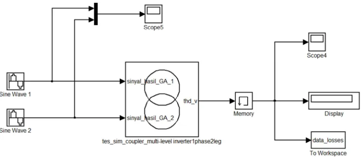
In this study, GA was used off‐line. The process of determining the parameters (Amplitude and phase shift angle) was done by running GA
program in Matlab software. For multilevel inverter system, the simulation
was done with PSIM software. Matlab and PSIM software run simultaneously
with “Simcoupler” module. In the process of simulation program path, then
the simulation would run alone with GA method, so we obtained the parameters (Amplitude and phase shift angle). For GA method, the
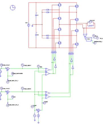
system shown in figure 5 and the “Simcoupler” module on PSIM was plant system multilevel inverter shown as figure 6.
Figure 5. Simulink Matlab for Plant System
After obtaining the parameters (Amplitude and phase shift angle), parameters were included in microcontroller programming (“Waijung microcontroller STM32F407 ARM Cortex”) as Amplitude and phase shift angle value to generate switching signal on switching component. The output voltage of the multilevel inverter was measured by using a power harmonic analyzer to determine the THD value.
The search process of optimization by genetic algorithm method was
done by using programming via MATLAB and PSIM, GA optimization process
was done on Matlab and main system simulated with PSIM. The two would
Figure 6. PSIM for Plant System Multilevel Inverter
5. EXPERIMENT AND ANALYSIS
5.1 Simulation Result Switching SPWM for Multilevel Inverter
In this system simulation design was done using PSIM as shown in
Figure 7. In this simulation, we used the DC source voltage parameters of 30 Volt DC by using a switch component of MOSFET. The test is carried out with
pure resistive load. Figure 8 is the condition of the switching Mosfet on the
Figure 7. Simulation PSIM Switching SPWM
Figure 8. Condition Switching S1, S2, S3, S4, S5, S6, S7 and S8
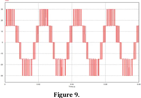
From the switching conditions, it generated output voltage from Multilevel Inverter Single‐Phase Three‐Level Diode Clamp Full Bridge shown as in figure 9 and the parameters as shown in table 2.
Figure 9.
Output Voltage Multilevel Inverter
Single‐Phase Three‐Level Diode Clamp Full Bridge
Table 2. Simulation Parameter
Parameter Value Parameter Value
V DC 24 Volt Frequency reference 50 Hz
Frequency 50 Hz Frequency carrier 1 KHz
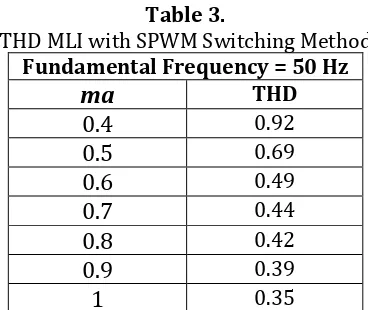
Figure 9 show that multilevel inverter voltage wave resulted THD data
as in table 3. Data was taken with ma (modulation index) which changed
from 0.4 up to 0.8. Harmonics were taken from n = 1 to n = 50 where the fundamental frequency was 50 Hz. Thus, the ranges of frequency were between 0 and 2500 Hz. As seen in table 3, the individual voltage harmonics
Table 3.
THD MLI with SPWM Switching Method Fundamental Frequency = 50 Hz
ma THD
0.4 0.92
0.5 0.69
0.6 0.49
0.7 0.44
0.8 0.42
0.9 0.39
1 0.35
The test was performed only on the change of the modulation index amplitude, because change the modulation index amplitude also affected the peak output voltage of the multilevel inverter in addition to the effect on THD. The modulation index amplitude is often used to get the output voltage from the multilevel inverter as needed. The modulation index frequency constantly used is the frequency of reference signal, that is 50 Hz and the frequency of carrier signal is 1 KHz. The value of the frequency will affect the switching capability of the component (MOSFET).
5.2 Testing Hardware Result Multilevel Inverter With SPWM
SPWM switching programming using Simulink Matlab with Waijung
library on Matlab which was then downloaded to the microcontroller. The
SPWM Simulink switching program is shown in Figure 10.
Result of switching can be seen as in figure 11.
Figure11. Switching SPWM Leg 1
Figure 11 shows the output of the SPWM switching signal for 1 leg. There are 4 switching for 1 leg. Reference signal is sinusoidal with frequency 50 Hz and triangle carrier signal with frequency 1 KHz. In Figure 12 is the output waveform of the multilevel inverter. The output voltage is measured by an oscilloscope to determine the shape of the voltage with DC voltage source of 24 volts dc.
Figure 12.Output Voltage Multilevel Inverter with SPWM Method
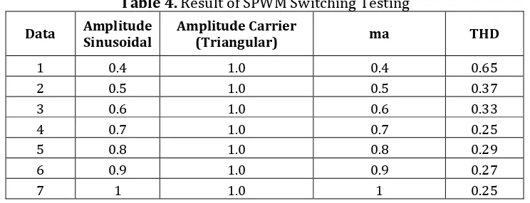
In multilevel inverter testing the data retrieval is done repeatedly based on the modulation index (ma). The data were taken with a range of modulation index 0.4 to 0.8. For the measurement results are shown as in table 4. THD tests limited to n = 50 means that calculations on measuring devices were only until harmonics to 50.
Table 4. Result of SPWM Switching Testing
Data Amplitude Sinusoidal
Amplitude Carrier
(Triangular) ma THD
1 0.4 1.0 0.4 0.65
2 0.5 1.0 0.5 0.37
3 0.6 1.0 0.6 0.33
4 0.7 1.0 0.7 0.25
5 0.8 1.0 0.8 0.29
6 0.9 1.0 0.9 0.27
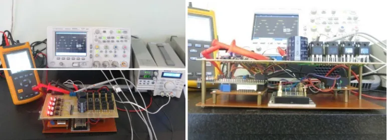
Measurement results with power harmonic analyzer and oscilloscope were shown as in figure 13. The measurement is done at ma = 1.
Figure 13. Result THD and Voltage of SPWM Switching Testing
On measurement with ma = 1 measured THD = 25.8% (0.258). In testing the tool was done using a measuring instrument in the form of oscilloscope and power harmonic analyzer. The image capture image is shown as shown in Figure 14.
Figure 14. Testing Hardware Multilevel Inverter Single Phase Three Level Full Bridge
5.3 Simulation Result Multilevel Inverter with Switching Modified PWM
Table 5. THD Modified PWM
Table 5 shows the result of PWM modified without GA. The result was obtained from trial and error. Trial was done with PSIM simulation. PWM modified process was done by adding sinusoidal signal with amplitude and certain frequency at 50 Hz sinusoidal reference signal. The added signal was sinusoidal with amplitude 0.1 and frequency 150 Hz for n = 3, 250 Hz for n = 5, 350 Hz for n = 7, 800 Hz for n = 16, 1100 Hz for n = 22, 1200 Hz for n = 24 and 2250 Hz for n = 45. From the data shown in table 5, PWM modified that had been done did not all produce better THD values than SPWM. In general the better result was a modified PWM on the addition of a signal with a frequency of 350 Hz for n = 7 and 1100 Hz for n = 22. After obtaining better THD from SPWM that was in addition of signal with frequency 350 Hz for n = 7 and 1100 Hz for n = 22, it was done a process to get best THD result by using GA. GA was used to obtain the correct amplitude and phase shift angle variables for signal enhancement, so that PWM modified signal could produce the best THD voltage that was minimum.
5.4 Simulation Result Multilevel Inverter with Switching Modified PWM and Genetic Algorithm Optimization
The optimization process with genetic algorithm was performed on signal modified with frequency 350 Hz for n = 7 and 1100 Hz for n = 22. The optimization process was done using genetic algorithm with the help of
Matlab. The data parameters in the genetic algorithm were chromosome = 2;
(a) (b)
Figure 15. (a) Graph Fitness For Modified PWM n=7 With GA ; ma = 0,8 (b) Graph Fitness For Modified PWM n=22 With GA ; ma = 0,4
Genetic algorithm optimization data of amplitude and phase shift angle magnitude are shown in table 6.
Table 6. Result Parameter with Genetic Algorithm Optimization
ma
From the results in table 6 above, the amplitude and phase shift angle were applied to the system so that the results are obtained THD as shown in table 7.
Table 7.
Result of THD with Genetic Algorithm Optimization
In figure 16 the sinusoidal signal image with amplitude of 0.0936 and a frequency of 350 Hz for n = 7 are added to the sinusoidal amplitude signal 0.8 and 50 Hz. Mathematically it can be shown like the following equation:
!7"#49= 87 728 = 0.8 !7#( + 0.0936 !7# 7( (14)
( = 2U ∗ = 2U ∗ 50
In figure 17 the picture of the sinusoidal signal with amplitude of 0.0991 and the frequency of 1100 Hz for n = 22 are added to the sinusoidal signal amplitude 0.8 and 50 Hz. Mathematically it can be shown like an
5.6 Testing Hardware Result Multilevel Inverter With Switching Modified PWM And Genetic Algorithm Optimization
Programming switching Modified PWM was done using Simulink with
library Waijung on Matlab that was then downloaded to microcontroller. The
Simulink program switching modified PWM is shown in figure 18. The test
Figure 18. Program Switching Simulink Modified PWM
Table 8.
Result of Testing Hardware Multilevel Inverter With Genetic Algorithm Optimization
n=7; f = 350 Hz n =22; f = 1100 Hz
ma Amplitude (Volt)
Phase Shift Angle
(rad)
THD ma Amplitude
(Volt)
Phase Shift Angle
(rad)
THD
0.4 0.0811 0 0.55 0.4 0.1221 0 0.57
0.5 0.0518 0 0.34 0.5 0.0954 1 0.43
0.6 0.0096 3 0.32 0.6 0.0406 1 0.33
0.7 0.0469 0 0.20 0.7 0.0998 0 0.30
0.8 0.0936 0 0.10 0.8 0.0991 0 0.29
Here is one example of the measured results as shown in figure 20 for PWM modified PWM n = 7 (f = 350 Hz) With Genetic Algorithm Optimization and figure 21 for modified PWM n = 22 (f = 1100 Hz) With Genetic Algorithm Optimization.
Figure 20. Result Output THD Voltage Modified PWM n = 7 (f=350 Hz) With GA Optimization
Figure 21. Result Output THD Voltage Modified PWM n = 22 (f=1100 Hz) With GA Optimization
5.7 Comparison SPWM, Modified PWM n = 7 (Frequency= 350 Hz) With Genetic Algorithm Optimization and Modified PWM n = 22 (Frequency =1100 Hz) With Genetic Algorithm Optimization
The simulation of comparison data is shown in table 9 and graph in figure 22. Comparison of THD simulation for PWM Modified n = 7 (Frequency = 350 Hz) with Genetic Algorithm Optimization and PWM Modified n = 22 (Frequency = 1100 Hz) with Genetic Algorithm Optimization is better than
SPWM. However, there are certain conditions in which ma results the same
result. Modified PWM n = 7 (Frequency = 350 Hz) Genetic Algorithm Optimization has maximum result, so minimum THD at m condition between 0.4 to 0.6 and modified PWM n = 22 (Frequency = 1100 Hz). Genetic
Algorithm Optimization has maximum result, so THD Minimum at ma
conditions were between 0.6 to 0.8. The data was taken with ma (modulation
Table 9. Simulation Result Comparison THD
ma
THD SPWM n =7 ; f =350 Hz
With GA
n = 22 ; f=1100 Hz With GA
0.4 0.91 0.89 0.84
0.5 0.68 0.67 0.63
0.6 0.49 0.48 0.48
0.7 0.44 0.41 0.43
0.8 0.42 0.38 0.42
THD Comparison Graph Simulation
Figure 22.Simulation Result THD Comparison Graph SPWM, Modified n = 7 (Frequency = 350 Hz) With GA Optimization and Modified n = 22 (Frequency = 1100
Hz) With GA Optimization
By testing the hardware, we obtained better THD results compared with SPWM. The results compare the data shown in Table 10 and the graph in Figure 23.
0.3 0.4 0.5 0.6 0.7 0.8 0.9
0 0.2 0.4 0.6 0.8 1
SPWM
350 GA
1100 GA
Table 10. Testing Hardware Result Comparison THD
Comparison of THD between SPWM, Modified PWM n = 7 (Frequency = 350 Hz) with Genetic Algorithm Optimization and modified PWM n = 22 (Frequency = 1100 Hz) with Genetic Algorithm Optimization was better than SPWM. Modified PWM n = 7 (Frequency = 350 Hz) with Genetic Algorithm Optimization resulted better results than SPWM, while Modified PWM n = 22 (Frequency = 1100 Hz) with Genetic Algorithm Optimization generated better THD under certain m conditions. The data was taken with ma (modulation index) varying from 0.4 to 0.8. Each ma has a different difference. The great decrease is at ma 0.8 where the THD decrease was with modified PWM n = 7 (Frequency = 350 Hz) with Genetic Algorithm Optimization up to 0.19 compared to SPWM While the biggest decrease was in modified PWM n = 22 (Frequency = 1100 Hz) with Genetic Algorithm Optimization When ma = 0.4 where the THD decrease to 0.08 compared with SPWM.
THD Comparison Graph Hardware
Figure 23.Testing Hardware Result THD Comparison Graph SPWM, Modified n = 7 (Frequency = 350 Hz) With GA Optimization and Modified n = 22 (Frequency =
Harmonic measurement and THD hardware test resulted different result because real measurement was done using power harmonic analyzer which have limitations in harmonic measurement that is only until harmonics to n = 50, whereas simulation of harmonic calculation can reach infinite frequency, that is until harmonic does not appear.
6. CONCLUSION
The modified PWM process using genetic algorithm method resulted in smaller THD voltage than SPWM switching. The optimization process was achieved by obtaining amplitude and phase shift angle variable of the established reference signal. The form of switching signal for reference signal was obtained by using genetic algorithm optimization method. Genetic Algorithm method is very effective in determining the best amplitude and angle variables used in the system since the optimum value can be selected from the many variables tested with Genetic Algorithm method on the computer. Genetic Algorithm method does not need many mathematical needs related to optimization because it will seek solutions based on natural evolution. By hardware testing, the result of modified PWM n = 7 (Frequency = 350 Hz) with Genetic Algorithm Optimization resulted in smaller THD compared with SPWM. The result of modified PWM n = 7 (Frequency = 350 Hz) with Genetic Algorithm Optimization got the best result of THD of 0.1 with modulation index 0.8 whereas modified PWM n = 22 (Frequency = 1100 Hz) with Genetic Algorithm Optimization got the best result of THD of 0.26
with modulation index 0.8. Each ma had a different difference. The great
decrease was at ma 0.8 where the THD decrease with modified PWM was n = 7 (Frequency = 350 Hz) with Genetic Algorithm Optimization up to 0.19 compared to SPWM While the biggest decrease was in modified PWM n = 22
(Frequency = 1100 Hz) with Genetic Algorithm Optimization was at ma = 0.4
where the THD decrease was to 0.08 compared with SPWM.
Acknowledgements
Firstly, I would like to thank the lecturers who always provide knowledge, support and lessons to me. Secondly, I would like to thank the applied post‐graduate program of EEPIS for providing facilities. Thirdly, I would like to thank the group of researcher in the Renewable Energy Laboratory and do not forget to thank my parents who always give a prayer for the success of my research.
REFERENCES
[1] Ahmet M Hava ; A High-Performance Generalized Discontinuous
PWM Algorithm ; IEEE TRANSACTIONS ON INDUSTRY APPLICATIONS, VOL. 34, NO. 5, SEPTEMBER/ OCTOBER 1998
[2] Abdelaziz Fri, R. E. (2013). CASCADED H-BRIDGE THREE-PHASE
DEDICATED TO PV. Journal of Theoretical and Applied Information Technology , Vol. 58 No.2, pp. 243‐249.
[3] Andreas Nordvall;Multilevel Inverter Topology Survey ; Master of
Science Thesis in Electric Power Engineering Department of Energy and
Environment Division of Electric Power Engineering CHALMERS
UNIVERSITY OF TECHNOLOGY Göteborg, Sweden, 2011
[4] Ardhia Wishnuprakasa, Era Purwanto, Novie Ayub Windarko,
Comparative Study of Modulation-Based Individual Inverter Techniques for Direct and Inverse by using Star-Connection Induction Motor in Extra Low Voltage Application; EMITTER International Journal of Engineering Technology;Vol. 4, No. 2, December 2016
[5] A. Shanmuga priyaa1, Dr. R. Seyezhai2, Dr. B. L. Mathur3, Performance
Analysis of Cascaded Z-Source Multilevel Inverter using Third Harmonic Injection PWM; International Journal of Computer Technology and Electronics Engineering (IJCTEE) Volume 2, Issue 1
[6] Changrong Liu jan,2005, A Novel High-Power High-Efficiency
Three-Phase Three-Phase-Shift DC/DC Converter For Fuel Cell Application ; Disertasi Faculty Of The Virginia Polytechnic Institute and state university, Zhong Du, L. M. (2006). A Cascade Multilevel Inverter Using a Single DC Source. IEEE , pp. 426‐430.
[7] C. R. Balamurugan, S. P. (2012). Investigations on Three Phase Five
Level Diode Clamped Multilevel Inverter, International Journal of Modern Engineering Research (IJMER) , Vol. 2 (Issue 3), pp. 1273‐1279.
[8] Deepak Shelar, P. K. (2014). High frequency modulated five level
diode clamped multilevel inverter fed three phase load by photovoltaic system, INTERNATIONAL CONFERENCE ON
COMPUTATION OF POWER, ENERGY, INFORMATION AND
COMMUNICATION (ICCPE IC) , pp. 468‐471.
[9] E. Sai Prateek Reddy, M. Ram Gopal Reddy, KRam Babu, BNishanth, Ch
Punya Venkata Varun, Cascaded MLI Operation for SPWM and Third
Harmonic SPWM, International Journal of Engineering Trends and Technology (IJETT) – Volume 11 Number 9 - May 2014
[10] José Rodríguez, Senior Member, IEEE, Jih‐Sheng Lai, Senior Member,
IEEE, and Fang Zheng Peng, Senior Member, IEEE ; Multilevel
Inverters: A Survey of [10] Topologies, Controls, and Applications; IEEE TRANSACTIONS ON INDUSTRIAL ELECTRONICS, VOL. 49, NO. 4, AUGUST 2002
[11] Jose Rodriguez ; Multilevel Voltage Source Converter Topologies for
Industrial Medium Voltage Drives ; IEEE Transactions On Industrial Electronic Vol. 54, No. 6 Dec 2007
[12] K.B.Nagasai, T.R.Jyothsna, Harmonic Analysis and Application of
[13] Kiruthika, S. ,. (2012), High Efficiency Three Phase Nine Level Diode Clamped Multilevel Inverter, International Journal of Science and Research (IJSR) , Vol. 1 (Issue 3), pp. 120‐123
[14] Leon M. Tolbert, Senior Member, IEEE, and Thomas G. Habetler, Senior
Member, IEEE; Novel Multilevel Inverter Carrier-Based PWM
Method ; IEEE TRANSACTIONS ON INDUSTRY APPLICATIONS, VOL. 35, NO. 5, SEPTEMBER/OCTOBER 1999
[15] M. Venu Madhav, K. R. (2012). MATLAB based Analysis and
Simulation of Multilevel Inverters. International Journal of Computer Applications , Vol. 39, pp. 17‐19.
[16] N.Mohan Teja, R S Ravi Sankar, P.Harsha, V. Uma Shankar; A Novel
Method of Diode Clamped Multi-Level Inverter using PWM Technique; International Journal of InventiveEngineeringand Sciences(IJIES) ISSN: 2319–9598, Volume‐2, Issue‐4,March 2014
[17] Nho Van Nguyen; An Optimized Discontinuous PWM Method to
Minimize Switching Loss for Multilevel Inverters; IEEE TRANSACTIONS ON INDUSTRIAL ELECTRONICS, VOL. 58, NO. 9, SEPTEMBER 2011
[18] Ony Asrarul Qudsi Novie Ayub Windarko Ardyono Priyadi Mauridhi
Hery Purnomo; Optimized GDPWM based on Spontaneous
Evolutionary GA for reducing switching losses on inverter ; IEEE Xplore: 02 December 2013
[19] Olorunfemi Ojo ; The Generalized Discontinuous PWM Scheme for
Three-Phase Voltage Source Inverters; IEEE TRANSACTIONS ON INDUSTRIAL ELECTRONICS, VOL. 51, NO. 6, DECEMBER 2004
[20] Phuong Hue Tran; Matlab/Simulink Implementation And Analysis Of
Three Pulse-Width-Modulation (Pwm) Techniques; A thesis submitted in partial fulfillment of the requirements for the degree of Master of Science in Electrical Engineering Boise State University May 2012
[21] Reza Salehi ;Elimination of Low Order Harmonic in Multilevel
Inverter Using Genetic Algorithm; Journal of Power Electronic Vol 11, No.2 March 2011
[22] Said Barkati ; Harmonic elimination in diode-clamped multilevel
inverter using evolutionary algorithms ; Elsevier/ScienceDirect; 7 may 2008 (1736‐1764)
[23] Srikanth, K. (2014). A Three Phase Multi Level Converter for grid
Connected PV. International Journal of Power Electronics and Drive System (IJPEDS) , Vol.5, pp. 71‐75.
[24] S.Shalini. (2013). Voltage Balancing in Diode Clamped Multilevel
Inverter Using Sinusoidal PWM. International Journal of Engineering Trends and Technology (IJETT) , Vol. 6, pp. 97‐103.
[25] V. Naga haskar Reddy, C. S. (2011). ADVANCED MODULATING
INDUCTION MOTOR. ARPN Journal of Engineering and Applied Sciences , Vol. 6 No. 1, pp. 90‐99.
[26] Xiaoming Yuan, Member, IEEE, and Ivo Barbi, Senior
Member,Fundamentals of a New Diode Clamping MultilevelInverter
;IEEE TRANSACTIONS ON POWER ELECTRONICS, VOL. 15, NO. 4, JULY 2000
[27] IEEE STD 519‐1992