Aripriharta, 2013. “
Smart Relay dan Aplikasinya”.
Malang: Graha Ilmu.
Anonim, 2002.
“Telemecanique Zelio-Logic Smart Relay”.
User’s Guide,
Schneider Electric.
Aripriharta, 2009. “
Buku Ajar PLC/Smart Relay”.
Malang: Graha Ilmu
Bolton William,alih bahasa Irzam Harmein. 2004. “
Programmable Logic Control
(PLC)” . Jakarta : Erlangga
Cripsin,Alan , 1990. “
Programmable Logic Control And Their Engineering
Aplication” .
London : Mc.Graw-Hill Book Company
Hidayat, Rizqi Rizaldi. 2011. “
Rancang Bangun Alat Pemisah Garam dan Air
Tawar Dengan Menggunakan Energi Matahari”
, Skripsi. Institut
Pertanian Bogor.
Santosa, Irfan dkk. 2010.
Pengaruh Kemiringan Kaca Pada Alat Basin Solar Still
Terhadap Kapasitas Air Hasil Destilasi,
Skripsi. Universitas Pancasakti.
http:// PLC CONTROL.com, diakses tanggal 25 April 2015 pukul 17:50.
http://www.vedcmalang.com/pppptkboemlg/index.php/menuutama/listrikelectro/9
54-rof diakses tanggal 19 Mei 2015 pukul 11: 13.
https://docs.google.com/document/Perencanaan Pengendali Ventilasi Jendela
Rumah Kaca Dengan Zelio Smart Relay /Jurnal Muhamad Hilman Akbar
5115122609 diakses tanggal 6 Juni 2015 pukul 15.46 .
https://duniakarya.wordpress.com/2009/08/21/merek-dan-
type
-
plc
/diakses tanggal
inf ormat ion provided in this document at ion cont ains general descript ions and/ or technical charac terist ics of the perf ormance of the product s cont ained herein. document at ion is not int ended as a subst itut e for and is not to be used for det ermining suit abi lit y or reliabilit y of these product s for specif ic user applicat ions. the dut y of any such user or int egrat or to perf orm the appropriat e and complet e risk analysis, evaluat ion and test ing of the product s wit h respect to the relevant specif ic applicat ion or use the reof . her Schneider Elect ric Indust ries SA S nor any of it s af filiat es or subsidiaries shall be respons ible or liable for misuse of the inf ormat ion cont ained herein.
DC - clock - display
Main
Range of product Zelio Logic Product or component
type Compact smart relay
[Us] rated supply
volt-age 24 V DC
Discrete input number 8 EN/IEC 61131-2 type 1 Analogue input number 4
Number of outputs 4 relay
Local display With
Clock With
Complementary
Supply current 100 mA without extension
Discrete input current 4 mA
Number or control scheme lines 120 ladder
≤ 200 FBD
Cycle time 6...90 ms
Backup time 10 years 25 °C
Clock drift 6 s/month 25 °C
12 min/year 0...55 °C
Checks Program memory on each power up
Supply voltage limits 19.2...30 V
Power dissipation in W 3 W without extension
Reverse polarity protection With
Discrete input type Resistive
Discrete input voltage 24 V DC
Counting frequency 1 kHz discrete input
Voltage state1 guaranteed ≥ 15 V IB...IG used as discrete input circuit ≥ 15 V I1...IA and IH...IR discrete input circuit Voltage state 0 guaranteed ≤ 5 V IB...IG used as discrete input circuit
≤ 5 V I1...IA and IH...IR discrete input circuit Current state 1 guaranteed ≥ 1.2 mA IB...IG used as discrete input circuit
≥ 2.2 mA I1...IA and IH...IR discrete input circuit Current state 0 guaranteed < 0.5 mA IB...IG used as discrete input circuit
< 0.75 mA I1...IA and IH...IR discrete input circuit
Input compatibility 3-wire proximity sensors PNP discrete input
Analogue input type Common mode
Analogue input range 0...10 V
0...24 V
Maximum permissible voltage 30 V analogue input circuit
Analogue input resolution 8 bits
LSB value 39 mV analogue input circuit
Conversion time Smart relay cycle time analogue input circuit
Conversion error +/- 5 % 25 °C analogue input circuit
+/- 6.2 % 55 °C analogue input circuit
Repeat accuracy +/- 2 % 55 °C analogue input circuit
Input impedance 7.4 kOhm I1...IA and IH...IR discrete input circuit 12 kOhm IB...IG used as analogue input circuit 12 kOhm IB...IG used as discrete input circuit
Output voltage limits 5...30 V DC relay output
24...250 V AC relay output
Contacts type and composition NO relay output
Output thermal current 8 A for all 4 outputs relay output
Electrical durability 500000 cycles DC-12 24 V 1.5 A relay output EN/IEC 60947-5-1 500000 cycles DC-13 24 V 0.6 A relay output EN/IEC 60947-5-1 500000 cycles AC-12 230 V 1.5 A relay output EN/IEC 60947-5-1 500000 cycles AC-15 230 V 0.9 A relay output EN/IEC 60947-5-1
Switching capacity in mA ≥ 10 mA 12 V relay output
Operating rate in Hz 0.1 Hz at Ie relay output
10 Hz no load relay output
Mechanical durability 10000000 cycles relay output
[Uimp] rated impulse withstand voltage 4 kV EN/IEC 60947-1 and EN/IEC 60664-1
Response time 5 ms from state 1 to state 0 relay output
10 ms from state 0 to state 1 relay output
Connections - terminals Screw terminals 1 x 0.25...1 x 2.5 mm² 24...14 flexible with cable end Screw terminals 2 x 0.2...2 x 1.5 mm² 24...16 solid
Screw terminals 1 x 0.2...1 x 2.5 mm² 25...14 solid Screw terminals 1 x 0.2...1 x 2.5 mm² 25...14 semi-solid
Screw terminals 2 x 0.25...2 x 0.75 mm² 24...18 flexible with cable end
Tightening torque 0.5 N.m
Overvoltage category III EN/IEC 60664-1
Product weight 0.25 kg
Environment
Immunity to microbreaks ≤ 1 ms
Product certifications C-Tick
CSA GL GOST UL
Standards EN/IEC 60068-2-27 Ea
EN/IEC 60068-2-6 Fc EN/IEC 61000-4-11 EN/IEC 61000-4-12 EN/IEC 61000-4-2 level 3 EN/IEC 61000-4-3 EN/IEC 61000-4-4 level 3 EN/IEC 61000-4-5 EN/IEC 61000-4-6 level 3
IP degree of protection IP20 terminal block IEC 60529
IP40 front panel IEC 60529
Environmental characteristic EMC directive EN/IEC 61131-2 zone B EMC directive EN/IEC 61000-6-2 EMC directive EN/IEC 61000-6-3 EMC directive EN/IEC 61000-6-4 Low voltage directive EN/IEC 61131-2 Disturbance radiated/conducted Class B EN 55022-11 group 1
Pollution degree 2 EN/IEC 61131-2
Ambient air temperature for operation -20...40 °C in non-ventilated enclosure IEC 60068-2-1 and IEC 60068-2-2 -20...55 °C IEC 60068-2-1 and IEC 60068-2-2
Ambient air temperature for storage -40...70 °C
Operating altitude 2000 m
Altitude transport ≤ 3048 m
Relative humidity 95 % without condensation or dripping water
RoHS EUR conformity date 0622
– 32 x 8 General Purpose Working Registers – Fully Static Operation
– Up to 16 MIPS Throughput at 16 MHz – On-chip 2-cycle Multiplier
• Nonvolatile Program and Data Memories
– 8K Bytes of In-System Self-Programmable Flash Endurance: 10,000 Write/Erase Cycles
– Optional Boot Code Section with Independent Lock Bits In-System Programming by On-chip Boot Program True Read-While-Write Operation
– 512 Bytes EEPROM
Endurance: 100,000 Write/Erase Cycles – 512 Bytes Internal SRAM
– Programming Lock for Software Security • Peripheral Features
– Two 8-bit Timer/Counters with Separate Prescalers and Compare Modes
– One 16-bit Timer/Counter with Separate Prescaler, Compare Mode, and Capture Mode
– Real Time Counter with Separate Oscillator – Four PWM Channels
– 8-channel, 10-bit ADC 8 Single-ended Channels
7 Differential Channels for TQFP Package Only
2 Differential Channels with Programmable Gain at 1x, 10x, or 200x for TQFP Package Only
– Byte-oriented Two-wire Serial Interface – Programmable Serial USART
– Master/Slave SPI Serial Interface
– Programmable Watchdog Timer with Separate On-chip Oscillator – On-chip Analog Comparator
• Special Microcontroller Features
– Power-on Reset and Programmable Brown-out Detection – Internal Calibrated RC Oscillator
– External and Internal Interrupt Sources
– Six Sleep Modes: Idle, ADC Noise Reduction, Power-save, Power-down, Standby and Extended Standby
• I/O and Packages
– 32 Programmable I/O Lines
– 40-pin PDIP, 44-lead TQFP, 44-lead PLCC, and 44-pad QFN/MLF • Operating Voltages
– 2.7 - 5.5V for ATmega8535L – 4.5 - 5.5V for ATmega8535 • Speed Grades
– 0 - 8 MHz for ATmega8535L – 0 - 16 MHz for ATmega8535
8-bit
Microcontroller
with 8K Bytes
In-System
Programmable
Flash
ATmega8535
ATmega8535L
Summary
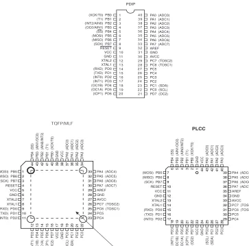
Pin Configurations
Figure 1. Pinout ATmega8535Disclaimer
Typical values contained in this data sheet are based on simulations and characteriza-tion of other AVR microcontrollers manufactured on the same process technology. Min and Max values will be available after the device is characterized.(XCK/T0) PB0 (T1) PB1 (INT2/AIN0) PB2 (OC0/AIN1) PB3 (SS) PB4 (MOSI) PB5 (MISO) PB6 (SCK) PB7 RESET VCC GND XTAL2 XTAL1 (RXD) PD0 (TXD) PD1 (INT0) PD2 (INT1) PD3 (OC1B) PD4 (OC1A) PD5 (ICP1) PD6
PA0 (ADC0) PA1 (ADC1) PA2 (ADC2) PA3 (ADC3) PA4 (ADC4) PA5 (ADC5) PA6 (ADC6) PA7 (ADC7) AREF GND AVCC PC7 (TOSC2) PC6 (TOSC1) PC5 PC4 PC3 PC2 PC1 (SDA) PC0 (SCL) PD7 (OC2)
1 2 3 4 5 6 7 8 9 10 11 33 32 31 30 29 28 27 26 25 24 23
(MOSI) PB5 (MISO) PB6 (SCK) PB7 RESET VCC GND XTAL2 XTAL1 (RXD) PD0 (TXD) PD1 (INT0) PD2
PA4 (ADC4) PA5 (ADC5) PA6 (ADC6) PA7 (ADC7) AREF GND AVCC PC7 (TOSC2) PC6 (TOSC1) PC5 PC4
44 43 42 41 40 39 38 37 36 35 34
12 13 14 15 16 17 18 19 20 21 22
(INT1) PD3 (OC1B) PD4 (OC1A) PD5 (ICP1) PD6 (OC2) PD7 VCC GND
(SCL) PC0 (SDA) PC1 PC2 PC3 PB4 (SS) PB3 (AIN1/OC0) PB2 (AIN0/INT2) PB1 (T1) PB0 (XCK/T0) GND VCC PA0 (ADC0) PA1 (ADC1) PA2 (ADC2) PA3 (ADC3)
7 8 9 10 11 12 13 14 15 16 17 39 38 37 36 35 34 33 32 31 30 29
(MOSI) PB5 (MISO) PB6 (SCK) PB7 RESET VCC GND XTAL2 XTAL1 (RXD) PD0 (TXD) PD1 (INT0) PD2
PA4 (ADC4) PA5 (ADC5) PA6 (ADC6) PA7 (ADC7) AREF GND AVCC PC7 (TOSC2) PC6 (TOSC1) PC5 PC4
6 5 4 3 2 1 44 43 42 41 40
18 19 20 21 22 23 24 25 26 27 28
(INT1) PD3 (OC1B) PD4 (OC1A) PD5 (ICP1) PD6 (OC2) PD7 VCC GND
(SCL) PC0 (SDA) PC1 PC2 PC3 PB4 (SS) PB3 (AIN1/OC0) PB2 (AIN0/INT2) PB1 (T1) PB0 (XCK/T0) GND VCC PA0 (ADC0) PA1 (ADC1) PA2 (ADC2) PA3 (ADC3)
PLCC
Overview
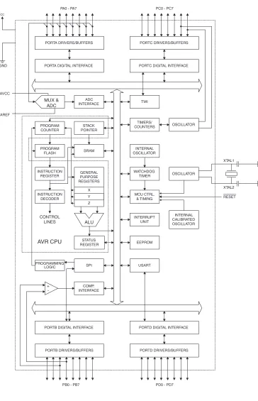
The ATmega8535 is a low-power CMOS 8-bit microcontroller based on the AVR enhanced RISC architecture. By executing instructions in a single clock cycle, the ATmega8535 achieves throughputs approaching 1 MIPS per MHz allowing the system designer to optimize power consumption versus processing speed.Block Diagram
Figure 2. Block DiagramINTERNAL OSCILLATOR
OSCILLATOR
WATCHDOG TIMER
MCU CTRL. & TIMING
OSCILLATOR TIMERS/
COUNTERS
INTERRUPT UNIT STACK
POINTER
EEPROM SRAM
STATUS REGISTER
USART PROGRAM
COUNTER
PROGRAM FLASH
INSTRUCTION REGISTER
INSTRUCTION DECODER
PROGRAMMING
LOGIC SPI
ADC INTERFACE
COMP. INTERFACE PORTA DRIVERS/BUFFERS
PORTA DIGITAL INTERFACE
GENERAL PURPOSE REGISTERS
X Y Z
ALU
+
-PORTC DRIVERS/BUFFERS
PORTC DIGITAL INTERFACE
PORTB DIGITAL INTERFACE
PORTB DRIVERS/BUFFERS
PORTD DIGITAL INTERFACE
PORTD DRIVERS/BUFFERS
XTAL1
XTAL2 RESET
CONTROL LINES
VCC
GND
MUX & ADC
AREF
PA0 - PA7 PC0 - PC7
PD0 - PD7 PB0 - PB7
AVR CPU
TWI AVCC
The AVR core combines a rich instruction set with 32 general purpose working registers. All 32 registers are directly connected to the Arithmetic Logic Unit (ALU), allowing two independent registers to be accessed in one single instruction executed in one clock cycle. The resulting architecture is more code efficient while achieving throughputs up to ten times faster than conventional CISC microcontrollers.
The ATmega8535 provides the following features: 8K bytes of In-System Programmable Flash with Read-While-Write capabilities, 512 bytes EEPROM, 512 bytes SRAM, 32 general purpose I/O lines, 32 general purpose working registers, three flexible Timer/Counters with compare modes, internal and external interrupts, a serial program-mable USART, a byte oriented Two-wire Serial Interface, an 8-channel, 10-bit ADC with optional differential input stage with programmable gain in TQFP package, a program-mable Watchdog Timer with Internal Oscillator, an SPI serial port, and six software selectable power saving modes. The Idle mode stops the CPU while allowing the SRAM, Timer/Counters, SPI port, and interrupt system to continue functioning. The Power-down mode saves the register contents but freezes the Oscillator, disabling all other chip functions until the next interrupt or Hardware Reset. In Power-save mode, the asynchronous timer continues to run, allowing the user to maintain a timer base while the rest of the device is sleeping. The ADC Noise Reduction mode stops the CPU and all I/O modules except asynchronous timer and ADC, to minimize switching noise during ADC conversions. In Standby mode, the crystal/resonator Oscillator is running while the rest of the device is sleeping. This allows very fast start-up combined with low-power consumption. In Extended Standby mode, both the main Oscillator and the asynchro-nous timer continue to run.
The device is manufactured using Atmel’s high density nonvolatile memory technology. The On-chip ISP Flash allows the program memory to be reprogrammed In-System through an SPI serial interface, by a conventional nonvolatile memory programmer, or by an On-chip Boot program running on the AVR core. The boot program can use any interface to download the application program in the Application Flash memory. Soft-ware in the Boot Flash section will continue to run while the Application Flash section is updated, providing true Read-While-Write operation. By combining an 8-bit RISC CPU with In-System Self-Programmable Flash on a monolithic chip, the Atmel ATmega8535 is a powerful microcontroller that provides a highly flexible and cost effective solution to many embedded control applications.
The ATmega8535 AVR is supported with a full suite of program and system develop-ment tools including: C compilers, macro assemblers, program debugger/simulators, In-Circuit Emulators, and evaluation kits.
AT90S8535 Compatibility
The ATmega8535 provides all the features of the AT90S8535. In addition, several new features are added. The ATmega8535 is backward compatible with AT90S8535 in most cases. However, some incompatibilities between the two microcontrollers exist. To solve this problem, an AT90S8535 compatibility mode can be selected by programming the S8535C fuse. ATmega8535 is pin compatible with AT90S8535, and can replace the AT90S8535 on current Printed Circuit Boards. However, the location of fuse bits and the electrical characteristics differs between the two devices.AT90S8535 Compatibility Mode
Programming the S8535C fuse will change the following functionality:
• The timed sequence for changing the Watchdog Time-out period is disabled. See “Timed Sequences for Changing the Configuration of the Watchdog Timer” on page 45 for details.
Pin Descriptions
VCC Digital supply voltage.
GND Ground.
Port A (PA7..PA0) Port A serves as the analog inputs to the A/D Converter.
Port A also serves as an 8-bit bi-directional I/O port, if the A/D Converter is not used. Port pins can provide internal pull-up resistors (selected for each bit). The Port A output buffers have symmetrical drive characteristics with both high sink and source capability. When pins PA0 to PA7 are used as inputs and are externally pulled low, they will source current if the internal pull-up resistors are activated. The Port A pins are tri-stated when a reset condition becomes active, even if the clock is not running.
Port B (PB7..PB0) Port B is an 8-bit bi-directional I/O port with internal pull-up resistors (selected for each bit). The Port B output buffers have symmetrical drive characteristics with both high sink and source capability. As inputs, Port B pins that are externally pulled low will source current if the pull-up resistors are activated. The Port B pins are tri-stated when a reset condition becomes active, even if the clock is not running.
Port B also serves the functions of various special features of the ATmega8535 as listed on page 60.
Port C (PC7..PC0) Port C is an 8-bit bi-directional I/O port with internal pull-up resistors (selected for each bit). The Port C output buffers have symmetrical drive characteristics with both high sink and source capability. As inputs, Port C pins that are externally pulled low will source current if the pull-up resistors are activated. The Port C pins are tri-stated when a reset condition becomes active, even if the clock is not running.
Port D (PD7..PD0) Port D is an 8-bit bi-directional I/O port with internal pull-up resistors (selected for each bit). The Port D output buffers have symmetrical drive characteristics with both high sink and source capability. As inputs, Port D pins that are externally pulled low will source current if the pull-up resistors are activated. The Port D pins are tri-stated when a reset condition becomes active, even if the clock is not running.
Port D also serves the functions of various special features of the ATmega8535 as listed on page 64.
RESET Reset input. A low level on this pin for longer than the minimum pulse length will
gener-ate a reset, even if the clock is not running. The minimum pulse length is given in Table 15 on page 37. Shorter pulses are not guaranteed to generate a reset.
XTAL1 Input to the inverting Oscillator amplifier and input to the internal clock operating circuit.
XTAL2 Output from the inverting Oscillator amplifier.
AVCC AVCC is the supply voltage pin for Port A and the A/D Converter. It should be externally connected to VCC, even if the ADC is not used. If the ADC is used, it should be
con-nected to VCC through a low-pass filter.
About Code
Examples
.
Register Summary
Address Name Bit 7 Bit 6 Bit 5 Bit 4 Bit 3 Bit 2 Bit 1 Bit 0 Page
0x3F (0x5F) SREG I T H S V N Z C 10
0x3E (0x5E) SPH – – – – – – SP9 SP8 12
0x3D (0x5D) SPL SP7 SP6 SP5 SP4 SP3 SP2 SP1 SP0 12
0x3C (0x5C) OCR0 Timer/Counter0 Output Compare Register 85
0x3B (0x5B) GICR INT1 INT0 INT2 – – – IVSEL IVCE 49, 69
0x3A (0x5A) GIFR INTF1 INTF0 INTF2 – – – – – 70
0x39 (0x59) TIMSK OCIE2 TOIE2 TICIE1 OCIE1A OCIE1B TOIE1 OCIE0 TOIE0 85, 115, 133
0x38 (0x58) TIFR OCF2 TOV2 ICF1 OCF1A OCF1B TOV1 OCF0 TOV0 86, 116, 134
0x37 (0x57) SPMCR SPMIE RWWSB – RWWSRE BLBSET PGWRT PGERS SPMEN 228
0x36 (0x56) TWCR TWINT TWEA TWSTA TWSTO TWWC TWEN – TWIE 181
0x35 (0x55) MCUCR SM2 SE SM1 SM0 ISC11 ISC10 ISC01 ISC00 32, 68
0x34 (0x54) MCUCSR – ISC2 – – WDRF BORF EXTRF PORF 40, 69
0x33 (0x53) TCCR0 FOC0 WGM00 COM01 COM00 WGM01 CS02 CS01 CS00 83
0x32 (0x52) TCNT0 Timer/Counter0 (8 Bits) 85
0x31 (0x51) OSCCAL Oscillator Calibration Register 30
0x30 (0x50) SFIOR ADTS2 ADTS1 ADTS0 – ACME PUD PSR2 PSR10 59,88,135,203,223
0x2F (0x4F) TCCR1A COM1A1 COM1A0 COM1B1 COM1B0 FOC1A FOC1B WGM11 WGM10 110
0x2E (0x4E) TCCR1B ICNC1 ICES1 – WGM13 WGM12 CS12 CS11 CS10 113
0x2D (0x4D) TCNT1H Timer/Counter1 – Counter Register High Byte 114
0x2C (0x4C) TCNT1L Timer/Counter1 – Counter Register Low Byte 114
0x2B (0x4B) OCR1AH Timer/Counter1 – Output Compare Register A High Byte 114
0x2A (0x4A) OCR1AL Timer/Counter1 – Output Compare Register A Low Byte 114
0x29 (0x49) OCR1BH Timer/Counter1 – Output Compare Register B High Byte 114
0x28 (0x48) OCR1BL Timer/Counter1 – Output Compare Register B Low Byte 114
0x27 (0x47) ICR1H Timer/Counter1 – Input Capture Register High Byte 114
0x26 (0x46) ICR1L Timer/Counter1 – Input Capture Register Low Byte 114
0x25 (0x45) TCCR2 FOC2 WGM20 COM21 COM20 WGM21 CS22 CS21 CS20 128
0x24 (0x44) TCNT2 Timer/Counter2 (8 Bits) 130
0x23 (0x43) OCR2 Timer/Counter2 Output Compare Register 131
0x22 (0x42) ASSR – – – – AS2 TCN2UB OCR2UB TCR2UB 131
0x21 (0x41) WDTCR – – – WDCE WDE WDP2 WDP1 WDP0 42
0x20(1) (0x40)(1) UBRRH URSEL – – – UBRR[11:8] 169
UCSRC URSEL UMSEL UPM1 UPM0 USBS UCSZ1 UCSZ0 UCPOL 167
0x1F (0x3F) EEARH – – – – – – – EEAR8 19
0x1E (0x3E) EEARL EEPROM Address Register Low Byte 19
0x1D (0x3D) EEDR EEPROM Data Register 19
0x1C (0x3C) EECR – – – – EERIE EEMWE EEWE EERE 19
0x1B (0x3B) PORTA PORTA7 PORTA6 PORTA5 PORTA4 PORTA3 PORTA2 PORTA1 PORTA0 66
0x1A (0x3A) DDRA DDA7 DDA6 DDA5 DDA4 DDA3 DDA2 DDA1 DDA0 66
0x19 (0x39) PINA PINA7 PINA6 PINA5 PINA4 PINA3 PINA2 PINA1 PINA0 66
0x18 (0x38) PORTB PORTB7 PORTB6 PORTB5 PORTB4 PORTB3 PORTB2 PORTB1 PORTB0 66
0x17 (0x37) DDRB DDB7 DDB6 DDB5 DDB4 DDB3 DDB2 DDB1 DDB0 66
0x16 (0x36) PINB PINB7 PINB6 PINB5 PINB4 PINB3 PINB2 PINB1 PINB0 67
0x15 (0x35) PORTC PORTC7 PORTC6 PORTC5 PORTC4 PORTC3 PORTC2 PORTC1 PORTC0 67
0x14 (0x34) DDRC DDC7 DDC6 DDC5 DDC4 DDC3 DDC2 DDC1 DDC0 67
0x13 (0x33) PINC PINC7 PINC6 PINC5 PINC4 PINC3 PINC2 PINC1 PINC0 67
0x12 (0x32) PORTD PORTD7 PORTD6 PORTD5 PORTD4 PORTD3 PORTD2 PORTD1 PORTD0 67
0x11 (0x31) DDRD DDD7 DDD6 DDD5 DDD4 DDD3 DDD2 DDD1 DDD0 67
0x10 (0x30) PIND PIND7 PIND6 PIND5 PIND4 PIND3 PIND2 PIND1 PIND0 67
0x0F (0x2F) SPDR SPI Data Register 143
0x0E (0x2E) SPSR SPIF WCOL – – – – – SPI2X 143
0x0D (0x2D) SPCR SPIE SPE DORD MSTR CPOL CPHA SPR1 SPR0 141
0x0C (0x2C) UDR USART I/O Data Register 164
0x0B (0x2B) UCSRA RXC TXC UDRE FE DOR PE U2X MPCM 165
0x0A (0x2A) UCSRB RXCIE TXCIE UDRIE RXEN TXEN UCSZ2 RXB8 TXB8 166
0x09 (0x29) UBRRL USART Baud Rate Register Low Byte 169
0x08 (0x28) ACSR ACD ACBG ACO ACI ACIE ACIC ACIS1 ACIS0 203
0x07 (0x27) ADMUX REFS1 REFS0 ADLAR MUX4 MUX3 MUX2 MUX1 MUX0 219
0x06 (0x26) ADCSRA ADEN ADSC ADATE ADIF ADIE ADPS2 ADPS1 ADPS0 221
0x05 (0x25) ADCH ADC Data Register High Byte 222
0x04 (0x24) ADCL ADC Data Register Low Byte 222
0x03 (0x23) TWDR Two-wire Serial Interface Data Register 183
0x02 (0x22) TWAR TWA6 TWA5 TWA4 TWA3 TWA2 TWA1 TWA0 TWGCE 183
Notes: 1. Refer to the USART description for details on how to access UBRRH and UCSRC.
2. For compatibility with future devices, reserved bits should be written to zero if accessed. Reserved I/O memory addresses should never be written.
3. Some of the status flags are cleared by writing a logical one to them. Note that the CBI and SBI instructions will operate on all bits in the I/O Register, writing a one back into any flag read as set, thus clearing the flag. The CBI and SBI instructions work with registers 0x00 to 0x1F only.
0x00 (0x20) TWBR Two-wire Serial Interface Bit Rate Register 181
Register Summary (Continued)
Instruction Set Summary
Mnemonics Operands Description Operation Flags #Clocks
ARITHMETIC AND LOGIC INSTRUCTIONS
ADD Rd, Rr Add two Registers Rd ← Rd + Rr Z,C,N,V,H 1
ADC Rd, Rr Add with Carry two Registers Rd ← Rd + Rr + C Z,C,N,V,H 1
ADIW Rdl,K Add Immediate to Word Rdh:Rdl ← Rdh:Rdl + K Z,C,N,V,S 2
SUB Rd, Rr Subtract two Registers Rd ← Rd - Rr Z,C,N,V,H 1
SUBI Rd, K Subtract Constant from Register Rd ← Rd - K Z,C,N,V,H 1
SBC Rd, Rr Subtract with Carry two Registers Rd ← Rd - Rr - C Z,C,N,V,H 1
SBCI Rd, K Subtract with Carry Constant from Reg. Rd ← Rd - K - C Z,C,N,V,H 1
SBIW Rdl,K Subtract Immediate from Word Rdh:Rdl ← Rdh:Rdl - K Z,C,N,V,S 2
AND Rd, Rr Logical AND Registers Rd ← Rd • Rr Z,N,V 1
ANDI Rd, K Logical AND Register and Constant Rd ← Rd • K Z,N,V 1
OR Rd, Rr Logical OR Registers Rd ← Rd v Rr Z,N,V 1
ORI Rd, K Logical OR Register and Constant Rd ← Rd v K Z,N,V 1
EOR Rd, Rr Exclusive OR Registers Rd ← Rd ⊕ Rr Z,N,V 1
COM Rd One’s Complement Rd ← 0xFF − Rd Z,C,N,V 1
NEG Rd Two’s Complement Rd ← 0x00 − Rd Z,C,N,V,H 1
SBR Rd,K Set Bit(s) in Register Rd ← Rd v K Z,N,V 1
CBR Rd,K Clear Bit(s) in Register Rd ← Rd • (0xFF - K) Z,N,V 1
INC Rd Increment Rd ← Rd + 1 Z,N,V 1
DEC Rd Decrement Rd ← Rd − 1 Z,N,V 1
TST Rd Test for Zero or Minus Rd ← Rd • Rd Z,N,V 1
CLR Rd Clear Register Rd ← Rd ⊕ Rd Z,N,V 1
SER Rd Set Register Rd ← 0xFF None 1
MUL Rd, Rr Multiply Unsigned R1:R0 ← Rd x Rr Z,C 2
MULS Rd, Rr Multiply Signed R1:R0 ← Rd x Rr Z,C 2
MULSU Rd, Rr Multiply Signed with Unsigned R1:R0 ← Rd x Rr Z,C 2
FMUL Rd, Rr Fractional Multiply Unsigned R1:R0 ← (Rd x Rr) << 1 Z,C 2
FMULS Rd, Rr Fractional Multiply Signed R1:R0 ← (Rd x Rr) << 1 Z,C 2
FMULSU Rd, Rr Fractional Multiply Signed with Unsigned R1:R0 ← (Rd x Rr) << 1 Z,C 2
BRANCH INSTRUCTIONS
RJMP k Relative Jump PC ← PC + k + 1 None 2
IJMP Indirect Jump to (Z) PC ← Z None 2
RCALL k Relative Subroutine Call PC ← PC + k + 1 None 3
ICALL Indirect Call to (Z) PC ←Z None 3
RET Subroutine Return PC ← STACK None 4
RETI Interrupt Return PC ← STACK I 4
CPSE Rd,Rr Compare, Skip if Equal if (Rd = Rr) PC ← PC + 2 or 3 None 1 / 2 / 3
CP Rd,Rr Compare Rd − Rr Z, N,V,C,H 1
CPC Rd,Rr Compare with Carry Rd − Rr − C Z, N,V,C,H 1
CPI Rd,K Compare Register with Immediate Rd − K Z, N,V,C,H 1
SBRC Rr, b Skip if Bit in Register Cleared if (Rr(b)=0) PC ← PC + 2 or 3 None 1 / 2 / 3
SBRS Rr, b Skip if Bit in Register is Set if (Rr(b)=1) PC ← PC + 2 or 3 None 1 / 2 / 3
SBIC P, b Skip if Bit in I/O Register Cleared if (P(b)=0) PC ← PC + 2 or 3 None 1 / 2 / 3
SBIS P, b Skip if Bit in I/O Register is Set if (P(b)=1) PC ← PC + 2 or 3 None 1 / 2 / 3
BRBS s, k Branch if Status Flag Set if (SREG(s) = 1) then PC←PC+k + 1 None 1 / 2
BRBC s, k Branch if Status Flag Cleared if (SREG(s) = 0) then PC←PC+k + 1 None 1 / 2
BREQ k Branch if Equal if (Z = 1) then PC ← PC + k + 1 None 1 / 2
BRNE k Branch if Not Equal if (Z = 0) then PC ← PC + k + 1 None 1 / 2
BRCS k Branch if Carry Set if (C = 1) then PC ← PC + k + 1 None 1 / 2
BRCC k Branch if Carry Cleared if (C = 0) then PC ← PC + k + 1 None 1 / 2
BRSH k Branch if Same or Higher if (C = 0) then PC ← PC + k + 1 None 1 / 2
BRLO k Branch if Lower if (C = 1) then PC ← PC + k + 1 None 1 / 2
BRMI k Branch if Minus if (N = 1) then PC ← PC + k + 1 None 1 / 2
BRPL k Branch if Plus if (N = 0) then PC ← PC + k + 1 None 1 / 2
BRGE k Branch if Greater or Equal, Signed if (N ⊕ V= 0) then PC ← PC + k + 1 None 1 / 2
BRLT k Branch if Less Than Zero, Signed if (N ⊕ V= 1) then PC ← PC + k + 1 None 1 / 2
BRHS k Branch if Half Carry Flag Set if (H = 1) then PC ← PC + k + 1 None 1 / 2
BRHC k Branch if Half Carry Flag Cleared if (H = 0) then PC ← PC + k + 1 None 1 / 2
BRTS k Branch if T Flag Set if (T = 1) then PC ← PC + k + 1 None 1 / 2
BRTC k Branch if T Flag Cleared if (T = 0) then PC ← PC + k + 1 None 1 / 2
BRVS k Branch if Overflow Flag is Set if (V = 1) then PC ← PC + k + 1 None 1 / 2
BRVC k Branch if Overflow Flag is Cleared if (V = 0) then PC ← PC + k + 1 None 1 / 2
BRIE k Branch if Interrupt Enabled if ( I = 1) then PC ← PC + k + 1 None 1 / 2
BRID k Branch if Interrupt Disabled if ( I = 0) then PC ← PC + k + 1 None 1 / 2
MOV Rd, Rr Move Between Registers Rd ← Rr None 1
MOVW Rd, Rr Copy Register Word Rd+1:Rd ← Rr+1:Rr None 1
LDI Rd, K Load Immediate Rd ←K None 1
LD Rd, X Load Indirect Rd ← (X) None 2
LD Rd, X+ Load Indirect and Post-Inc. Rd ← (X), X ← X + 1 None 2
LD Rd, - X Load Indirect and Pre-Dec. X ← X - 1, Rd ← (X) None 2
LD Rd, Y Load Indirect Rd ← (Y) None 2
LD Rd, Y+ Load Indirect and Post-Inc. Rd ← (Y), Y ← Y + 1 None 2
LD Rd, - Y Load Indirect and Pre-Dec. Y ← Y - 1, Rd ← (Y) None 2
LDD Rd,Y+q Load Indirect with Displacement Rd ← (Y + q) None 2
LD Rd, Z Load Indirect Rd ← (Z) None 2
LD Rd, Z+ Load Indirect and Post-Inc. Rd ← (Z), Z ← Z+1 None 2
LD Rd, -Z Load Indirect and Pre-Dec. Z ← Z - 1, Rd ← (Z) None 2
LDD Rd, Z+q Load Indirect with Displacement Rd ← (Z + q) None 2
LDS Rd, k Load Direct from SRAM Rd ← (k) None 2
ST X, Rr Store Indirect (X) ← Rr None 2
ST X+, Rr Store Indirect and Post-Inc. (X) ← Rr, X ← X + 1 None 2
ST - X, Rr Store Indirect and Pre-Dec. X ← X - 1, (X) ← Rr None 2
ST Y, Rr Store Indirect (Y) ← Rr None 2
ST Y+, Rr Store Indirect and Post-Inc. (Y) ← Rr, Y ← Y + 1 None 2
ST - Y, Rr Store Indirect and Pre-Dec. Y ← Y - 1, (Y) ← Rr None 2
STD Y+q,Rr Store Indirect with Displacement (Y + q) ← Rr None 2
ST Z, Rr Store Indirect (Z) ← Rr None 2
ST Z+, Rr Store Indirect and Post-Inc. (Z) ← Rr, Z ← Z + 1 None 2
ST -Z, Rr Store Indirect and Pre-Dec. Z ← Z - 1, (Z) ← Rr None 2
STD Z+q,Rr Store Indirect with Displacement (Z + q) ← Rr None 2
STS k, Rr Store Direct to SRAM (k) ← Rr None 2
LPM Load Program Memory R0 ← (Z) None 3
LPM Rd, Z Load Program Memory Rd ← (Z) None 3
LPM Rd, Z+ Load Program Memory and Post-Inc Rd ← (Z), Z ← Z+1 None 3
SPM Store Program Memory (Z) ← R1:R0 None
-IN Rd, P In Port Rd ←P None 1
OUT P, Rr Out Port P ← Rr None 1
PUSH Rr Push Register on Stack STACK ← Rr None 2
POP Rd Pop Register from Stack Rd ← STACK None 2
BIT AND BIT-TEST INSTRUCTIONS
SBI P,b Set Bit in I/O Register I/O(P,b) ←1 None 2
CBI P,b Clear Bit in I/O Register I/O(P,b) ←0 None 2
LSL Rd Logical Shift Left Rd(n+1) ← Rd(n), Rd(0) ← 0 Z,C,N,V 1
LSR Rd Logical Shift Right Rd(n) ← Rd(n+1), Rd(7) ← 0 Z,C,N,V 1
ROL Rd Rotate Left Through Carry Rd(0)←C,Rd(n+1)← Rd(n),C←Rd(7) Z,C,N,V 1
ROR Rd Rotate Right Through Carry Rd(7)←C,Rd(n)← Rd(n+1),C←Rd(0) Z,C,N,V 1
ASR Rd Arithmetic Shift Right Rd(n) ← Rd(n+1), n=0..6 Z,C,N,V 1
SWAP Rd Swap Nibbles Rd(3..0)←Rd(7..4),Rd(7..4)←Rd(3..0) None 1
BSET s Flag Set SREG(s) ← 1 SREG(s) 1
BCLR s Flag Clear SREG(s) ← 0 SREG(s) 1
BST Rr, b Bit Store from Register to T T ← Rr(b) T 1
BLD Rd, b Bit load from T to Register Rd(b) ←T None 1
SEC Set Carry C ←1 C 1
CLC Clear Carry C ← 0 C 1
SEN Set Negative Flag N ←1 N 1
CLN Clear Negative Flag N ← 0 N 1
SEZ Set Zero Flag Z ←1 Z 1
CLZ Clear Zero Flag Z ← 0 Z 1
SEI Global Interrupt Enable I ←1 I 1
CLI Global Interrupt Disable I ← 0 I 1
SES Set Signed Test Flag S ←1 S 1
CLS Clear Signed Test Flag S ← 0 S 1
SEV Set Twos Complement Overflow. V ←1 V 1
CLV Clear Twos Complement Overflow V ← 0 V 1
SET Set T in SREG T ←1 T 1
CLT Clear T in SREG T ← 0 T 1
SEH Set Half Carry Flag in SREG H ←1 H 1
CLH Clear Half Carry Flag in SREG H ← 0 H 1
MCU CONTROL INSTRUCTIONS
NOP No Operation None 1
SLEEP Sleep (see specific descr. for Sleep function) None 1
WDR Watchdog Reset (see specific descr. for WDR/Timer) None 1
BREAK Break For On-chip Debug Only None N/A
Ordering Information
Note: 1. This device can also be supplied in wafer form. Please contact your local Atmel sales office for detailed ordering information and minimum quantities..
2. Pb-free packaging alternative, complies to the European Directive for Restriction of Hazardous Substances (RoHS direc-tive).Also Halide free and fully Green.
Speed (MHz) Power Supply Ordering Code Package(1) Operation Range
8 2.7 - 5.5V
ATmega8535L-8AC ATmega8535L-8PC ATmega8535L-8JC ATmega8535L-8MC
44A 40P6 44J 44M1
Commercial (0°C to 70°C)
ATmega8535L-8AI ATmega8535L-8PI ATmega8535L-8JI ATmega8535L-8MI ATmega8535L-8AU(2)
ATmega8535L-8PU(2) ATmega8535L-8JU(2)
ATmega8535L-8MU(2)
44A 40P6 44J 44M1 44A 40P6 44J 44M1
Industrial (-40°C to 85°C)
16 4.5 - 5.5V
ATmega8535-16AC ATmega8535-16PC ATmega8535-16JC ATmega8535-16MC
44A 40P6 44J 44M1
Commercial (0°C to 70°C)
ATmega8535-16AI ATmega8535-16PI ATmega8535-16JI ATmega8535-16MI ATmega8535-16AU(2)
ATmega8535-16PU(2) ATmega8535-16JU(2)
ATmega8535-16MU(2)
44A 40P6 44J 44M1 44A 40P6 44J 44M1
Industrial (-40°C to 85°C)
Package Type
44A 44-lead, Thin (1.0 mm) Plastic Gull Wing Quad Flat Package (TQFP)
40P6 40-pin, 0.600” Wide, Plastic Dual Inline Package (PDIP)
44J 44-lead, Plastic J-leaded Chip Carrier (PLCC)
Packaging Information
44A
2325 Orchard Parkway San Jose, CA 95131
TITLE DRAWING NO.
R
REV. 44A, 44-lead, 10 x 10 mm Body Size, 1.0 mm Body Thickness,
0.8 mm Lead Pitch, Thin Profile Plastic Quad Flat Package (TQFP) 44A B 10/5/2001 PIN 1 IDENTIFIER
0˚~7˚ PIN 1
L C
A1 A2 A
D1 D
e E1 E
B
COMMON DIMENSIONS
(Unit of Measure = mm)
SYMBOL MIN NOM MAX NOTE
Notes: 1. This package conforms to JEDEC reference MS-026, Variation ACB. 2. Dimensions D1 and E1 do not include mold protrusion. Allowable
protrusion is 0.25 mm per side. Dimensions D1 and E1 are maximum plastic body size dimensions including mold mismatch.
3. Lead coplanarity is 0.10 mm maximum.
A – – 1.20
A1 0.05 – 0.15
A2 0.95 1.00 1.05
D 11.75 12.00 12.25
D1 9.90 10.00 10.10 Note 2
E 11.75 12.00 12.25
E1 9.90 10.00 10.10 Note 2
B 0.30 – 0.45
C 0.09 – 0.20
L 0.45 – 0.75
40P6
2325 Orchard Parkway San Jose, CA 95131
TITLE DRAWING NO.
R
REV. 40P6, 40-lead (0.600"/15.24 mm Wide) Plastic Dual
Inline Package (PDIP) 40P6 B
09/28/01 PIN
1
E1
A1 B
REF E
B1
C L
SEATING PLANE
A
0º ~ 15º D
e
eB
COMMON DIMENSIONS
(Unit of Measure = mm)
SYMBOL MIN NOM MAX NOTE
A – – 4.826
A1 0.381 – –
D 52.070 – 52.578 Note 2
E 15.240 – 15.875
E1 13.462 – 13.970 Note 2
B 0.356 – 0.559
B1 1.041 – 1.651
L 3.048 – 3.556
C 0.203 – 0.381
eB 15.494 – 17.526
e 2.540 TYP
Notes: 1. This package conforms to JEDEC reference MS-011, Variation AC. 2. Dimensions D and E1 do not include mold Flash or Protrusion.
44J
Notes: 1. This package conforms to JEDEC reference MS-018, Variation AC. 2. Dimensions D1 and E1 do not include mold protrusion.
Allowable protrusion is .010"(0.254 mm) per side. Dimension D1 and E1 include mold mismatch and are measured at the extreme material condition at the upper or lower parting line.
3. Lead coplanarity is 0.004" (0.102 mm) maximum.
A 4.191 – 4.572
A1 2.286 – 3.048
A2 0.508 – –
D 17.399 – 17.653
D1 16.510 – 16.662 Note 2
E 17.399 – 17.653
E1 16.510 – 16.662 Note 2
D2/E2 14.986 – 16.002
B 0.660 – 0.813
B1 0.330 – 0.533
e 1.270 TYP
COMMON DIMENSIONS
(Unit of Measure = mm)
SYMBOL MIN NOM MAX NOTE
1.14(0.045) X 45˚ PIN NO. 1 IDENTIFIER
1.14(0.045) X 45˚
0.51(0.020)MAX
0.318(0.0125) 0.191(0.0075)
A2
45˚ MAX (3X)
A
A1
B1 D2/E2
B
e
E1 E
D1
D
44J, 44-lead, Plastic J-leaded Chip Carrier (PLCC) 44J B 10/04/01
2325 Orchard Parkway San Jose, CA 95131
TITLE DRAWING NO.
R
44M1-A
2325 Orchard Parkway San Jose, CA 95131
TITLE DRAWING NO.
R
REV. 44M1, 44-pad, 7 x 7 x 1.0 mm Body, Lead Pitch 0.50 mm,
G 44M1
5/27/06
COMMON DIMENSIONS
(Unit of Measure = mm)
SYMBOL MIN NOM MAX NOTE
A 0.80 0.90 1.00
A1 – 0.02 0.05
A3 0.25 REF
b 0.18 0.23 0.30
D
D2 5.00 5.20 5.40
6.90 7.00 7.10 6.90 7.00 7.10
E
E2 5.00 5.20 5.40
e 0.50 BSC
L 0.59 0.64 0.69
K 0.20 0.26 0.41 Note: JEDEC Standard MO-220, Fig. 1 (SAW Singulation) VKKD-3.
TOP VIEW
SIDE VIEW
BOTTOM VIEW D
E Marked Pin# 1 ID
E2
D2
b e
Pin #1 Corner L
A1
A3
A
SEATING PLANE
Pin #1 Triangle
Pin #1 Chamfer (C 0.30)
Option A
Option B
Pin #1 Notch (0.20 R)
Option C
K
K
1 2
3
Errata
The revision letter refer to the device revision.ATmega8535
Rev. A and B
• First Analog Comparator conversion may be delayed • Asynchronous Oscillator does not stop in Power-down
1. First Analog Comparator conversion may be delayed
If the device is powered by a slow rising VCC, the first Analog Comparator
conver-sion will take longer than expected on some devices.
Problem Fix/Workaround
When the device has been powered or reset, disable then enable the Analog Com-parator before the first conversion.
2. Asynchronous Oscillator does not stop in Power-down
The asynchronous oscillator does not stop when entering Power-down mode. This leads to higher power consumption than expected.
Problem Fix/Workaround
Datasheet Revision
History
Please note that the referring page numbers in this section are referring to this docu-ment. The referring revision in this section are referring to the document revision.
Changes from Rev.
2502J- 08/06 to Rev.
2502K- 10/06
1. Updated TOP/BOTTOM description for all Timer/Counters Fast PWM mode.
2. Updated “Errata” on page 18.
Changes from Rev.
2502I- 06/06 to Rev.
2502J- 08/06
1. Updated “Ordering Information” on page 13.
Changes from Rev.
2502H- 04/06 to Rev.
2502I- 06/06
1. Updated code example “USART Initialization” on page 150.
Changes from Rev.
2502G- 04/05 to Rev.
2502H- 04/06
1. Added “Resources” on page 6.
2. Updated Table 7 on page 29, Table 17 on page 42 and Table 111 on page 258.
3. Updated “Serial Peripheral Interface – SPI” on page 136.
4. Updated note in “Bit Rate Generator Unit” on page 180.
Changes from Rev.
2502F- 06/04 to Rev.
2502G- 04/05
1. Removed “Preliminary” and TBD’s.
2. Updated Table 37 on page 69 and Table 113 on page 261.
3. Updated “Electrical Characteristics” on page 255.
4. Updated “Ordering Information” on page 13.
Changes from Rev.
2502E-12/03 to Rev.
2502G-06/04
1. MLF-package alternative changed to “Quad Flat No-Lead/Micro Lead Frame
Package QFN/MLF”.
Changes from Rev.
2502E-12/03 to Rev.
2502F-06/04
1. Updated “Reset Characteristics” on page 37.
2. Updated SPH in “Stack Pointer” on page 12.
3. Updated C code in “USART Initialization” on page 150.
4. Updated “Errata” on page 18.
Changes from Rev.
2502D-09/03 to Rev.
2502E-12/03
1. Updated “Calibrated Internal RC Oscillator” on page 29.
Changes from Rev.
2502C-04/03 to Rev.
2502D-09/03
1. Removed “Advance Information” and some TBD’s from the datasheet.
2. Added note to “Pinout ATmega8535” on page 2.
3. Updated “Reset Characteristics” on page 37.
4. Updated “Absolute Maximum Ratings” and “DC Characteristics” in “Electrical
Characteristics” on page 255.
5. Updated Table 111 on page 258.
6. Updated “ADC Characteristics” on page 263.
7. Updated “ATmega8535 Typical Characteristics” on page 266.
8. Removed CALL and JMP instructions from code examples and “Instruction
Set Summary” on page 10.
Changes from Rev.
2502B-09/02 to Rev.
2502C-04/03
1. Updated “Packaging Information” on page 14.
2. Updated Figure 1 on page 2, Figure 84 on page 179, Figure 85 on page 185,
Figure 87 on page 191, Figure 98 on page 207.
3. Added the section “EEPROM Write During Power-down Sleep Mode” on page
22.
4. Removed the references to the application notes “Multi-purpose Oscillator”
and “32 kHz Crystal Oscillator”, which do not exist.
5. Updated code examples on page 44.
6. Removed ADHSM bit.
7. Renamed Port D pin ICP to ICP1. See “Alternate Functions of Port D” on page 64.
8. Added information about PWM symmetry for Timer 0 on page 79 and Timer 2
on page 126.
9. Updated Table 68 on page 169, Table 75 on page 190, Table 76 on page 193,
Table 77 on page 196, Table 108 on page 253, Table 113 on page 261.
10. Updated description on “Bit 5 – TWSTA: TWI START Condition Bit” on page 182.
11. Updated the description in “Filling the Temporary Buffer (Page Loading)” and “Performing a Page Write” on page 231.
12. Removed the section description in “SPI Serial Programming Characteristics” on page 254.
14. Updated “ADC Characteristics” on page 263.
14. Updated “Register Summary” on page 8.
15. Various Timer 1 corrections.
16. Added WD_FUSE period in Table 108 on page 253.
Changes from Rev.
2502A-06/02 to Rev.
2502B-09/02
Disclaimer: The information in this document is provided in connection with Atmel products. No license, express or implied, by estoppel or otherwise, to any intellectual property right is granted by this document or in connection with the sale of Atmel products. EXCEPT AS SET FORTH IN ATMEL’S TERMS AND CONDI-TIONS OF SALE LOCATED ON ATMEL’S WEB SITE, ATMEL ASSUMES NO LIABILITY WHATSOEVER AND DISCLAIMS ANY EXPRESS, IMPLIED OR STATUTORY WARRANTY RELATING TO ITS PRODUCTS INCLUDING, BUT NOT LIMITED TO, THE IMPLIED WARRANTY OF MERCHANTABILITY, FITNESS FOR A PARTICULAR PURPOSE, OR NON-INFRINGEMENT. IN NO EVENT SHALL ATMEL BE LIABLE FOR ANY DIRECT, INDIRECT, CONSEQUENTIAL, PUNITIVE, SPECIAL OR INCIDEN-TAL DAMAGES (INCLUDING, WITHOUT LIMITATION, DAMAGES FOR LOSS OF PROFITS, BUSINESS INTERRUPTION, OR LOSS OF INFORMATION) ARISING OUT OF THE USE OR INABILITY TO USE THIS DOCUMENT, EVEN IF ATMEL HAS BEEN ADVISED OF THE POSSIBILITY OF SUCH DAMAGES. Atmel makes no representations or warranties with respect to the accuracy or completeness of the contents of this document and reserves the right to make changes to specifications and product descriptions at any time without notice. Atmel does not make any commitment to update the information contained herein. Atmel’s products are not intended, authorized, or warranted for use as components in applications intended to support or sustain life.
Atmel Corporation
Atmel Operations
2325 Orchard Parkway San Jose, CA 95131, USA Tel: 1(408) 441-0311 Fax: 1(408) 487-2600
Regional Headquarters
Europe
Atmel Sarl
Route des Arsenaux 41 Case Postale 80 CH-1705 Fribourg Switzerland
Tel: (41) 26-426-5555 Fax: (41) 26-426-5500
Asia
Room 1219
Chinachem Golden Plaza 77 Mody Road Tsimshatsui East Kowloon
Hong Kong
Tel: (852) 2721-9778 Fax: (852) 2722-1369
Japan
9F, Tonetsu Shinkawa Bldg. 1-24-8 Shinkawa
Chuo-ku, Tokyo 104-0033 Japan
Tel: (81) 3-3523-3551 Fax: (81) 3-3523-7581
Memory
2325 Orchard Parkway San Jose, CA 95131, USA Tel: 1(408) 441-0311 Fax: 1(408) 436-4314
Microcontrollers
2325 Orchard Parkway San Jose, CA 95131, USA Tel: 1(408) 441-0311 Fax: 1(408) 436-4314
La Chantrerie BP 70602
44306 Nantes Cedex 3, France Tel: (33) 2-40-18-18-18
Fax: (33) 2-40-18-19-60
ASIC/ASSP/Smart Cards
Zone Industrielle
13106 Rousset Cedex, France Tel: (33) 4-42-53-60-00 Fax: (33) 4-42-53-60-01
1150 East Cheyenne Mtn. Blvd. Colorado Springs, CO 80906, USA Tel: 1(719) 576-3300
Fax: 1(719) 540-1759
Scottish Enterprise Technology Park Maxwell Building
East Kilbride G75 0QR, Scotland Tel: (44) 1355-803-000
Fax: (44) 1355-242-743
RF/Automotive
Theresienstrasse 2 Postfach 3535
74025 Heilbronn, Germany Tel: (49) 71-31-67-0 Fax: (49) 71-31-67-2340
1150 East Cheyenne Mtn. Blvd. Colorado Springs, CO 80906, USA Tel: 1(719) 576-3300
Fax: 1(719) 540-1759
Biometrics/Imaging/Hi-Rel MPU/ High Speed Converters/RF Datacom
Avenue de Rochepleine BP 123
38521 Saint-Egreve Cedex, France Tel: (33) 4-76-58-30-00
Fax: (33) 4-76-58-34-80
Literature Requests
www.atmel.com/literature
© 2006 Atmel Corporation. All rights reserved. Atmel®, logo and combinations thereof, Everywhere You Are®, AVR®, and others are the
Page 1 of The enclosed information is believed to be correct, Information may change ‘without notice’ due to
product improvement. Users should ensure that the product is suitable for their use. E. & O. E.
Revision A 04/07/2003 Power Supplies and Meters
Power Supplies and Meters
Power Supplies and Meters
Power Supplies and Meters
Power Supplies and Meters
Order code Order code Order code
Order code Manufacturer codeManufacturer codeManufacturer codeManufacturer code DescriptionDescriptionDescriptionDescription
78-1084 SRF04 ULTRASONIC RANGE FINDER (RE)
Sensors & Transducers
Ultrasonic range finder SRF04
Specification
Parameter Details
Voltage 5V
Current 30mA Typ. 50mA Max
Frequency 40kHz
Max. Range 3m
Min. Range 3cm
Sensitivity Detects a 3cm diameter broom handle at > 2m Input Trigger 10µS Min. TTL level pulse
Echo Pulse Positive TTL level signal. Width proportional to range
Dimensions 43mm x 20mm x 17 height
Pin Configurations
General Description
The DS18S20 digital thermometer provides 9-bit Celsius temperature measurements and has an alarm function with nonvolatile user-programmable upper and lower trig-ger points. The DS18S20 communicates over a 1-Wire bus that by definition requires only one data line (and ground) for communication with a central microproces-sor. It has an operating temperature range of –55°C to +125°C and is accurate to ±0.5°C over the range of –10°C to +85°C. In addition, the DS18S20 can derive power directly from the data line (“parasite power”), eliminating the need for an external power supply.
Each DS18S20 has a unique 64-bit serial code, which allows multiple DS18S20s to function on the same 1-Wire bus. Thus, it is simple to use one microprocessor to control many DS18S20s distributed over a large area. Applications that can benefit from this feature include HVAC environmental controls, temperature monitoring systems inside buildings, equipment, or machinery, and process monitoring and control systems.
Applications
● Thermostatic Controls
● Industrial Systems
● Consumer Products
● Thermometers
● Thermally Sensitive Systems
Benefits and Features
● Unique 1-Wire® Interface Requires Only One Port
Pin for Communication
● Maximize System Accuracy in Broad Range of Thermal Management Applications
• Measures Temperatures from -55°C to +125°C (-67°F to +257°F)
• ±0.5°C Accuracy from -10°C to +85°C • 9-Bit Resolution
• No External Components Required
● Parasite Power Mode Requires Only 2 Pins for Operation (DQ and GND)
● Simplifies Distributed Temperature-Sensing Applications with Multidrop Capability
• Each Device Has a Unique 64-Bit Serial Code Stored in On-Board ROM
● Flexible User-Definable Nonvolatile (NV) Alarm Settings with Alarm Search Command Identifies Devices with Temperatures Outside Programmed Limits
● Available in 8-Pin SO (150 mils) and 3-Pin TO-92 Packages
Ordering Information appears at end of data sheet.
1-Wire is a registered trademark of Maxim Integrated Products, Inc.
BOTTOM VIEW 2 N.C. N.C. VDD GND N.C. N.C. N.C. GND DS18S20
SO (150 mils) (DS18S20Z) + 1 4 3 7 8 5 6 DS18S20
1 2 3
GND DQ VDD
1 1 2 3
TOP VIEW
Voltage Range on Any Pin Relative to Ground ....-0.5V to +6.0V Continuous Power Dissipation (TA = +70°C)
8-Pin SO (derate 5.9mW/°C above +70°C) ...470.6mW 3-Pin TO-92 (derate 6.3mW/°C above +70°C) ...500mW Operating Temperature Range ... -55°C to +125°C
Storage Temperature Range ... -55°C to +125°C Lead Temperature (soldering, 10s) ... +260°C Soldering Temperature (reflow)
Lead(Pb)-free... .+260°C Containing lead(Pb) ... +240°C
Note 1: All voltages are referenced to ground.
Note 2: The Pullup Supply Voltage specification assumes that the pullup device is ideal, and therefore the high level of the
pul-lup is equal to VPU. In order to meet the VIH spec of the DS18S20, the actual supply rail for the strong pullup transistor must include margin for the voltage drop across the transistor when it is turned on; thus: VPU_ACTUAL = VPU_IDEAL + VTRANSISTOR.
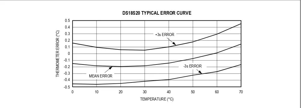
Note 3: See typical performance curve in Figure 1.
Note 4: Logic-low voltages are specified at a sink current of 4mA.
Note 5: To guarantee a presence pulse under low voltage parasite power conditions, VILMAX may have to be reduced to as
low as 0.5V.
Note 6: Logic-high voltages are specified at a source current of 1mA.
Note 7: Standby current specified up to +70°C. Standby current typically is 3µA at +125°C.
Note 8: To minimize IDDS, DQ should be within the following ranges: GND ≤ DQ ≤ GND + 0.3V or VDD – 0.3V ≤ DQ ≤ VDD.
Note 9: Active current refers to supply current during active temperature conversions or EEPROM writes.
Note 10: DQ line is high (“high-Z” state).
Note 11: Drift data is based on a 1000-hour stress test at +125°C with VDD = 5.5V.
(VDD = 3.0V to 5.5V, TA = -55°C to +125°C, unless otherwise noted.)
PARAMETER SYMBOL CONDITIONS MIN TYP MAX UNITS
Supply Voltage VDD Local Power (Note 1) +3.0 +5.5 V
Pullup Supply Voltage VPU Parasite Power (Note 1, 2) +3.0 +5.5 V
Local Power +3.0 VDD
Thermometer Error tERR -10°C to +85°C (Note 3) ±0.5 °C
-55°C to +125°C ±2
Input Logic-Low VIL (Note 1, 4, 5) -0.3 +0.8 V
Input Logic-High VIH
Local Power
(Note 1, 6)
+2.2 The lower of 5.5 or VDD
+ 0.3
V
Parasite Power +3.0
Sink Current IL VI/O = 0.4V (Note 1) 4.0 mA
Standby Current IDDS (Note 7, 8) 750 1000 nA
Active Current IDD VDD = 5V (Note 9) 1 1.5 mA
DQ Input Current IDQ (Note 10) 5 µA
Drift (Note 11) ±0.2 °C
DS18S20
High-Precision 1-Wire Digital Thermometer
Absolute Maximum Ratings
These are stress ratings only and functional operation of the device at these or any other conditions above those indicated in the operation sections of this specification is not implied. Exposure to absolute maximum rating conditions for extended periods of time may affect reliability.
(VDD = 3.0V to 5.5V, TA = -55°C to +100°C, unless otherwise noted.)
(VDD = 3.0V to 5.5V; TA = -55°C to +125°C, unless otherwise noted.)
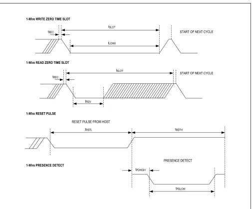
Note 12: See the timing diagrams in Figure 2.
Note 13: Under parasite power, if tRSTL > 960µs, a power-on reset may occur.
PARAMETER SYMBOL CONDITIONS MIN TYP MAX UNITS
NV Write Cycle Time tWR 2 10 ms
EEPROM Writes NEEWR -55°C to +55°C 50k writes
EEPROM Data Retention tEEDR -55°C to +55°C 10 years
PARAMETER SYMBOL CONDITIONS MIN TYP MAX UNITS
Temperature Conversion Time tCONV (Note 12) 750 ms
Time to Strong Pullup On tSPON Start Convert T Command Issued 10 µs
Time Slot tSLOT (Note 12) 60 120 µs
Recovery Time tREC (Note 12) 1 µs
Write 0 Low Time tLOW0 (Note 12) 60 120 µs
Write 1 Low Time tLOW1 (Note 12) 1 15 µs
Read Data Valid tRDV (Note 12) 15 µs
Reset Time High tRSTH (Note 12) 480 µs
Reset Time Low tRSTL (Note 12, 13) 480 µs
Presence-Detect High tPDHIGH (Note 12) 15 60 µs
Presence-Detect Low tPDLOW (Note 12) 60 240 µs
Capacitance CIN/OUT 25 pF
Figure 1. Typical Performance Curve
DS18S20 TYPICAL ERROR CURVE
0.5 0.4 0.3 0.2 0.1 0 -0.1 -0.2 -0.3 -0.4
-0.5
THERMOMETER ERROR (°C)
0 10 20 30 40 50 60 70
TEMPERATURE (°C) +3s ERROR
MEAN ERROR
-3s ERROR
AC Electrical Characteristics—NV Memory
PIN
NAME FUNCTION
TO-92 SO
1 5 GND Ground
2 4 DQ Data Input/Output. Open-drain 1-Wire interface pin. Also provides power to the device when used in parasite power mode (see the Powering the DS18S20 section.)
3 3 VDD Optional VDD. VDD must be grounded for operation in parasite power mode.
— 1, 2, 6, 7, 8 N.C. No Connection Figure 2. Timing Diagrams
START OF NEXT CYCLE
1-Wire WRITE ZERO TIME SLOT
tREC
tSLOT
tLOW0
1-Wire READ ZERO TIME SLOT
tREC
tSLOT
START OF NEXT CYCLE
tRDV
1-Wire RESET PULSE
1-Wire PRESENCE DETECT
tRSTL tRSTH
tPDHIGH
PRESENCE DETECT
tPDLOW RESET PULSE FROM HOST
DS18S20
High-Precision 1-Wire Digital Thermometer
Overview
Figure 3 shows a block diagram of the DS18S20, and pin descriptions are given in the Pin Description table. The 64-bit ROM stores the device’s unique serial code. The scratchpad memory contains the 2-byte temperature register that stores the digital output from the temperature sensor. In addition, the scratchpad provides access to the 1-byte upper and lower alarm trigger registers (TH and TL). The TH and TL registers are nonvolatile (EEPROM), so they will retain data when the device is powered down.
The DS18S20 uses Maxim’s exclusive 1-Wire bus proto-col that implements bus communication using one control signal. The control line requires a weak pullup resistor since all devices are linked to the bus via a 3-state or open-drain port (the DQ pin in the case of the DS18S20). In this bus system, the microprocessor (the master device) identifies and addresses devices on the bus using each device’s unique 64-bit code. Because each device has a unique code, the number of devices that can be addressed on one bus is virtually unlimited. The 1-Wire bus protocol, including detailed explanations of the commands and “time slots,” is covered in the 1-Wire Bus System section.
Another feature of the DS18S20 is the ability to operate without an external power supply. Power is instead sup-plied through the 1-Wire pullup resistor via the DQ pin when the bus is high. The high bus signal also charges an
internal capacitor (CPP), which then supplies power to the device when the bus is low. This method of deriving power from the 1-Wire bus is referred to as “parasite power.” As an alternative, the DS18S20 may also be powered by an external supply on VDD.
Operation—Measuring Temperature
The core functionality of the DS18S20 is its direct-to-dig-ital temperature sensor. The temperature sensor output has 9-bit resolution, which corresponds to 0.5°C steps. The DS18S20 powers-up in a low-power idle state; to initiate a temperature measurement and A-to-D conver-sion, the master must issue a Convert T [44h] command. Following the conversion, the resulting thermal data is stored in the 2-byte temperature register in the scratch-pad memory and the DS18S20 returns to its idle state. If the DS18S20 is powered by an external supply, the master can issue “read-time slots” (see the 1-Wire Bus System section) after the Convert T command and the DS18S20 will respond by transmitting 0 while the tem-perature conversion is in progress and 1 when the con-version is done. If the DS18S20 is powered with parasite power, this notification technique cannot be used since the bus must be pulled high by a strong pullup during the entire temperature conversion. The bus requirements for parasite power are explained in detail in the Powering The DS18S20 section.
Figure 3. DS18S20 Block Diagram VPU 64-BIT ROM AND 1-Wire PORT DQ VDD INTERNAL VDD CPP
PARASITE POWER CIRCUIT MEMORY
CONTROL LOGIC SCRATCHPAD 8-BIT CRC GENERATOR TEMPERATURE SENSOR
ALARM HIGH TRIGGER (TH) REGISTER (EEPROM)
ALARM LOW TRIGGER (TL) REGISTER (EEPROM) GND
DS18S20
4.7kΩ
The DS18S20 output data is calibrated in degrees cen-tigrade; for Fahrenheit applications, a lookup table or conversion routine must be used. The temperature data is stored as a 16-bit sign-extended two’s complement num-ber in the temperature register (see Figure 4). The sign bits (S) indicate if the temperature is positive or negative: for positive numbers S = 0 and for negative numbers S = 1. Table 1 gives examples of digital output data and the corresponding temperature reading.
Resolutions greater than 9 bits can be calculated using the data from the temperature, COUNT REMAIN and COUNT PER °C registers in the scratchpad. Note that the COUNT PER °C register is hard-wired to 16 (10h). After reading the scratchpad, the TEMP_READ value is obtained by truncating the 0.5°C bit (bit 0) from the temperature data (see Figure 4). The extended resolution temperature can then be calculated using the following equation:
TEMPERATURE TEMP_READ 0.25
COUNT_PER_C COUNT_REMAIN
COUNT_PER_C
= −
− +
Operation—Alarm Signaling
After the DS18S20 performs a temperature conversion, the temperature value is compared to the user-defined two’s complement alarm trigger values stored in the 1-byte TH and TL registers (see Figure 5). The sign bit (S) indicates if the value is positive or negative: for positive numbers S = 0 and for negative numbers S = 1. The TH and TL registers are nonvolatile (EEPROM) so they will retain data when the device is powered down. TH and TL can be accessed through bytes 2 and 3 of the scratchpad as explained in the Memory section.
Only bits 8 through 1 of the temperature register are used in the TH and TL comparison since TH and TL are 8-bit registers. If the measured temperature is lower than or equal to TL or higher than TH, an alarm condition exists and an alarm flag is set inside the DS18S20. This flag is updated after every temperature measurement; therefore, if the alarm condition goes away, the flag will be turned off after the next temperature conversion.
Table 1. Temperature/Data Relationship
TEMPERATURE (°C) DIGITAL OUTPUT (BINARY) DIGITAL OUTPUT (HEX)
+85.0* 0000 0000 1010 1010 00AAh
+25.0 0000 0000 0011 0010 0032h
+0.5 0000 0000 0000 0001 0001h
0 0000 0000 0000 0000 0000h
-0.5 1111 1111 1111 1111 FFFFh
-25.0 1111 1111 1100 1110 FFCEh
-55.0 1111 1111 1001 0010 FF92h
Figure 4. Temperature Register Format
Figure 5. TH and TL Register Format
BIT 7 BIT 6 BIT 5 BIT 4 BIT 3 BIT 2 BIT 1 BIT 0
LS BYTE 26 25 24 23 22 21 20 2-1
BIT 15 BIT 14 BIT 13 BIT 12 BIT 11 BIT 10 BIT 9 BIT 8
MS BYTE S S S S S S S S
S = SIGN
BIT 7 BIT 6 BIT 5 BIT 4 BIT 3 BIT 2 BIT 1 BIT 0
S 26 25 25 25 22 21 20
The master device can check the alarm flag status of all DS18S20s on the bus by issuing an Alarm Search [ECh] command. Any DS18S20s with a set alarm flag will respond to the command, so the master can determine exactly which DS18S20s have experienced an alarm condition. If an alarm condition exists and the TH or TL settings have changed, another temperature conversion should be done to validate the alarm condition.
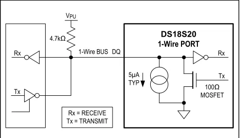
Powering The DS18S20
The DS18S20 can be powered by an external supply on the VDD pin, or it can operate in “parasite power” mode, which allows the DS18S20 to function without a local external supply. Parasite power is very useful for applica-tions that require remote temperature sensing or those with space constraints. Figure 3 shows the DS18S20’s parasite-power control circuitry, which “steals” power from the 1-Wire bus via the DQ pin when the bus is high. The stolen charge powers the DS18S20 while the bus is high, and some of the charge is stored on the parasite power capacitor (CPP) to provide power when the bus is low. When the DS18S20 is used in parasite power mode, the VDD pin must be connected to ground.
In parasite power mode, the 1-Wire bus and CPP can provide sufficient current to the DS18S20 for most opera-tions as long as the specified timing and voltage require-ments are met (see the DC Electrical Characteristics
and the AC Electrical Characteristics). However, when the DS18S20 is performing temperature conversions or copying data from the scratchpad memory to EEPROM, the operating current can be as high as 1.5mA. This current can cause an unacceptable voltage drop across the weak 1-Wire pullup resistor and is more current than can be supplied by CPP. To assure that the DS18S20 has sufficient supply current, it is necessary to provide a strong pullup on the 1-Wire bus whenever temperature
conversions are taking place or data is being copied from the scratchpad to EEPROM. This can be accomplished by using a MOSFET to pull the bus directly to the rail as shown in Figure 6. The 1-Wire bus must be switched to the strong pullup within 10µs (max) after a Convert T [44h] or Copy Scratchpad [48h] command is issued, and the bus must be held high by the pullup for the duration of the conversion (tCONV) or data transfer (tWR = 10ms). No other activity can take place on the 1-Wire bus while the pullup is enabled.
The DS18S20 can also be powered by the conventional method of connecting an external power supply to the VDD pin, as shown in Figure 7. The advantage of this method is that the MOSFET pullup is not required, and the 1-Wire bus is free to carry other traffic during the tem-perature conversion time.
The use of parasite power is not recommended for tem-peratures above 100°C since the DS18S20 may not be able to sustain communications due to the higher leak-age currents that can exist at these temperatures. For applications in which such temperatures are likely, it is strongly recommended that the DS18S20 be powered by an external power supply.
In some situations the bus master may not know whether the DS18S20s on the bus are parasite powered or pow-ered by external supplies. The master needs this informa-tion to determine if the strong bus pullup should be used during temperature conversions. To get this information, the master can issue a Skip ROM [CCh] command fol-lowed by a Read Power Supply [B4h] command folfol-lowed by a “read-time slot”. During the read-time slot, parasite powered DS18S20s will pull the bus low, and externally powered DS18S20s will let the bus remain high. If the bus is pulled low, the master knows that it must supply the strong pullup on the 1-Wire bus during temperature conversions.
Figure 6. Supplying the Parasite-Powered DS18S20 During Temperature Conversions
Figure 7. Powering the DS18S20 with an External Supply VPU
4.7kΩ VPU
1-Wire BUS
DS18S20
GND DQ VDD
TO OTHER 1-Wire DEVICES µP VDD (EXTERNAL SUPPLY) VPU 4.7kΩ 1-Wire BUS
DS18S20
GND DQ VDD
64-Bit Lasered ROM Code
Each DS18S20 contains a unique 64-bit code (see Figure 8) stored in ROM. The least significant 8 bits of the ROM code contain the DS18S20’s 1-Wire family code: 10h. The next 48 bits contain a unique serial number. The most significant 8 bits contain a cyclic redundancy check (CRC) byte that is calculated from the first 56 bits of the ROM code. A detailed explanation of the CRC bits is provided in the CRC Generation section. The 64-bit ROM code and associated ROM function control logic allow the DS18S20 to operate as a 1-Wire device using the protocol detailed in the 1-Wire Bus System section.
Memory
The DS18S20’s memory is organized as shown in Figure 9. The memory consists of an SRAM scratch-pad with nonvolatile EEPROM storage for the high and low alarm trigger registers (TH and TL). Note that if the DS18S20 alarm function is not used, the TH and TL reg-isters can serve as general-purpose memory. All mem-ory commands are described in detail in the DS18S20 Function Commands section.
Byte 0 and byte 1 of the scratchpad contain the LSB and the MSB of the temperature register, respectively. These bytes are read-only. Bytes 2 and 3 provide access to TH and TL registers. Bytes 4 and 5 are reserved for internal use by the device and cannot be overwritten; these bytes will return all 1s when read. Bytes 6 and 7 contain the COUNT REMAIN and COUNT PER ºC registers, which can be used to calculate extended resolution results as
explained in the Operation—Measuring Temperature
section.
Byte 8 of the scratchpad is read-only and contains the CRC code for bytes 0 through 7 of the scratchpad. The DS18S20 generates this CRC using the method described in the CRC Generation section.
Data is written to bytes 2 and 3 of the scratchpad using the Write Scratchpad [4Eh] command; the data must be transmitted to the DS18S20 starting with the least signifi-cant bit of byte 2. To verify data integrity, the scratchpad can be read (using the Read Scratchpad [BEh] command) after the data is written. When reading the scratchpad, data is transferred over the 1-Wire bus starting with the least significant bit of byte 0. To transfer the TH and TL data from the scratchpad to EEPROM, the master must issue the Copy Scratchpad [48h] command.
Figure 8. 64-Bit Lasered ROM Code
Figure 9. DS18S20 Memory Map
8-BIT CRC 48-BIT SERIAL NUMBER 8-BIT FAMILY CODE (10h)
MSB LSB MSB LSB MSB LSB
BYTE 0
BYTE 1
TEMPERATURE LSB (AAh)
TEMPERATURE MSB (00h) (85°C)
BYTE 2
BYTE 3
TH REGISTER OR USER BYTE 1*
TL REGISTER OR USER BYTE 2*
BYTE 4
BYTE 5
RESERVED (FFh)
RESERVED (FFh)
BYTE 6
BYTE 7
COUNT REMAIN (0Ch)
COUNT PER °C (10h)
BYTE 8 CRC*
*POWER-UP STATE DEPENDS ON VALUE(S) STORED IN EEPROM.
TH REGISTER OR USER BYTE 1
TL REGISTER OR USER BYTE 2
SCRATCHPAD (POWER-UP STATE)
EEPROM
Data in the EEPROM registers is retained when the device is powered down; at power-up the EEPROM data is reloaded into the corresponding scratchpad locations. Data can also be reloaded from EEPROM to the scratch-pad at any time using the Recall E2 [B8h] command. The master can issue “read-time slots” (see the 1-Wire Bus System section) following the Recall E2 command
and the DS18S20 will indicate the status of the recall by transmitting 0 while the recall is in progress and 1 when the recall is done.
CRC Generation
CRC bytes are provided as part of the DS18S20’s 64-bit ROM code and in the 9th byte of the scratchpad memory. The ROM code CRC is calculated from the first 56 bits of the ROM code and is contained in the most significant byte of the ROM. The scratchpad CRC is calculated from the data stored in the scratchpad, and therefore it chang-es when the data in the scratchpad changchang-es. The CRCs provide the bus master with a method of data validation when data is read from the DS18S20. To verify that data has been read correctly, the bus master must re-cal