TM 6
ISSUES TO ADDRESS...
• What types of defects arise in solids?
• Can the number and type of defects be varied and controlled?
• How do defects afect material properties?
• Are defects undesirable?
Defects in Solids
Why Study Imperfection in Solids?
1. Properties of Materials are profoundly
influenced by the presence of imperfection
2. Mechanical properties of metals
•
Solidifcation
- result of casting of molten
material
–
2 steps
• Nuclei form
• Nuclei grow to form crystals – grain structure
•
Start with a molten material – all liquid
Imperfections in Solids
Adapted from Fig.4.14 (b), Callister 7e.
• Crystals grow until they meet each other
Polycrystalline Materials
Grain Boundaries
•
regions between crystals
•
transition from lattice of
one region to that of the
other
•
slightly disordered
•
low density in grain
boundaries
– high mobility – high difusivity
– high chemical reactivity
Solidifcation
Columnar in
area with less
undercooling
Shell of
equiaxed
grains due to
rapid cooling
(greater
T
)
near wall
heat
flow
Grains can be
- equiaxed (roughly same size in all
directions)
- columnar (elongated grains)
Adapted from Fig. 4.12, Callister 7e.
Imperfections in Solids
There is no such thing as a perfect
crystal.
•
What are these imperfections?
•
Why are they important?
• Vacancy atoms
• Interstitial atoms
• Substitutional atoms
Point defects
Types of Imperfections
• Dislocations
Line defects
• Vacancies:
-vacant atomic sites in a structure.
• Self-Interstitials:
-"extra" atoms positioned between atomic sites.
Point Defects
Vacancy
distortion
of planes
self-interstitial
Boltzmann's constant
No. of defects
No. of potential defect sites.
Activation energy
Temperature
Each lattice site is a potential
vacancy site
• Equilibrium concentration varies with temperature!
• We can get Qv from
Measuring Activation Energy
• Find the equil. # of vacancies in 1 m3 of Cu at 1000C.
• Given:
A Cu = 63.5 g/mol
r = 8.4 g / cm 3
Q v = 0.9 eV/atom N A = 6.02 x 10²³ atoms/mol
Estimating Vacancy Concentration
• Low energy electron
Reprinted with permission from Nature (K.F. McCarty, J.A. Nobel, and N.C. Bartelt, "Vacancies in
Solids and the Stability of Surface Morphology", Nature, Vol. 412, pp. 622-625 (2001). Image is 5.75 mm by 5.75 mm.) Copyright (2001) Macmillan Publishers, Ltd.
Observing Equilibrium Vacancy Conc.
I
Two outcomes if impurity (B) added to host (A):
•
Solid solution
of
B
in
A
(i.e., random dist. of point
defects)
• Solid solution of
B
in
A
plus particles of a new
phase (usually for a larger amount of B)
OR
Substitutional
solid
soln.
(e.g.,
Cu
in
Ni
)
Interstitial
solid
soln.
(e.g.,
C
in
Fe
)
Second phase particle
--diferent
composition
--often diferent structure.
Imperfections in Solids
Conditions for substitutional solid
solution (S.S.)
•
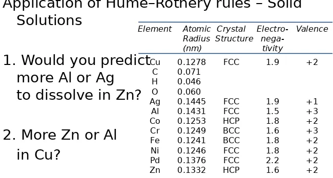
W. Hume – Rothery rule
–
1.
r
(atomic radius) < 15%
–
2. Proximity in periodic table
•
i.e., similar electronegativities
–
3. Same crystal structure for pure metals
–
4. Valency
•
All else being equal, a metal will have a greater
Imperfections in Solids
Application of Hume–Rothery rules – Solid
Solutions
1. Would you predict
more Al or Ag
to dissolve in Zn?
2. More Zn or Al
in Cu?
Table on p. 106, Callister 7e.
Element Atomic Crystal Electro- Valence Radius Structure
Imperfections in Solids
•
Specifcation of composition
–
weight percent
• are line defects,
• slip between crystal planes result when dislocations
move,
• produce permanent (plastic) deformation.
Dislocations
:
Schematic of Zinc (HCP):
• before deformation
• after tensile elongation
slip steps
Line Defects
Imperfections in Solids
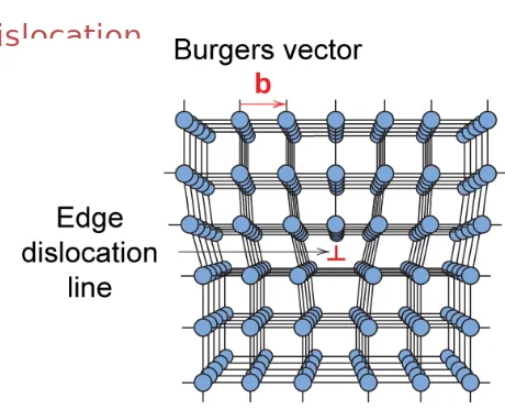
Linear Defects (
Dislocations
)
–
Are one-dimensional defects around which atoms are
misaligned
•
Edge dislocation:
–
extra half-plane of atoms inserted in a crystal
structure
–
b
to dislocation line
•
Screw dislocation:
–
spiral planar ramp resulting from shear deformation
–
b
to dislocation line
Imperfections in Solids
Fig. 4.3, Callister 7e.
• Dislocation motion requires the successive bumping of a half plane of atoms (from left to right here). • Bonds across the slipping planes are broken and remade in succession.
Atomic view of edge dislocation motion from left to right as a crystal is sheared.
Imperfections in Solids
Screw Dislocation
Adapted from Fig. 4.4, Callister 7e.
Burgers vector
b
Dislocation line
b
(a)
(b)
Edge, Screw, and Mixed Dislocations
Edge
Screw
Imperfections in Solids
Dislocations are visible in electron
micrographs
Dislocations & Crystal Structures
• Structure: close-packed
planes & directions are preferred.
view onto two close-packed planes.
close-packed plane (bottom)
close-packed plane (top)
close-packed directions
• Comparison among crystal structures:
FCC: many close-packed planes/directions;
HCP: only one plane, 3 directions;
BCC: none
• Specimens that were tensile
tested.
Mg (HCP)
Al (FCC)
Planar Defects in Solids
•One case is a twin boundary (plane)
–Essentially a reflection of atom positions across the twin plane.
•Stacking faults
–For FCC metals an error in ABCABC packing sequence
–Ex: ABCABABC
Dislocations & Materials Classes
• Covalent Ceramics
(Si, diamond): Motion hard.
-directional (angular) bonding
• Ionic Ceramics (NaCl):
Motion hard.
• Metals: Disl. motion easier.
-non-directional bonding
-close-packed directions
for slip.
electron cloud
ion cores
Dislocation Motion
Dislocations & plastic deformation
•
Cubic & hexagonal metals - plastic
deformation by
plastic shear or slip
where one
plane of atoms slides over adjacent plane by
defect motion (dislocations).
• If dislocations don't move,
Dislocation Motion
•
Dislocation moves along
slip plane
in
slip
direction
perpendicular to dislocation line
•
Slip direction same direction as
Burgers vector
Edge dislocation
Screw dislocation
34
Slip System
–
Slip plane
- plane allowing easiest slippage
• Wide interplanar spacings - highest planar densities
–
Slip direction
- direction of movement -
Highest
linear densities
–
FCC Slip occurs on {111} planes (close-packed) in
<110> directions (close-packed)
=> total of 12 slip systems in FCC
Deformation Mechanisms
Stress has units:
Elastic means reversible!
Elastic Deformation
1. Initial 2. Small load 3. Unload
F
d
bonds
stretch
return to
initial
F
d
Linear-
elastic
Plastic means permanent!
Plastic Deformation (Metals)
F
d
linear
elastic linear elastic
1. Initial 2. Small load 3. Unload
p lanes still
sheared
F
d elastic + plastic
bonds stretch
& planes shear
(at lower temperatures, i.e.
T
<
T
melt/3)
Plastic (Permanent) Deformation
• Simple tension test:
engineering stress,
s
engineering strain,
e
Elastic+Plastic
at larger stress
permanent (plastic)
after load is removed
e
pplastic strain
Elastic
initially
Stress and Dislocation Motion
• Crystals slip due to a resolved shear stress, tR. • Applied tension can produce such a stress.
slip plane normal, ns
Resolved shear
stress:
t
R=
Fs
/
As
Relation between
s
and
t
RApplied tensile
Microscopic Examination
•
Crystallites (grains) and grain
boundaries. Vary considerably in size.
Can be quite large
–
ex: Large single crystal of quartz or
diamond or Si
–
ex: Aluminum light post or garbage can -
see the individual grains
•
Crystallites (grains) can be quite small
• Useful up to 2000X magnifcation.
• Polishing removes surface features (e.g., scratches) • Etching changes reflectance, depending on crystal orientation.
Micrograph of
brass (a Cu-Zn alloy)
Optical Microscopy
Adapted from Fig. 4.13(b) and (c),
Callister 7e. (Fig. 4.13(c) is courtesy of J.E. Burke, General Electric Co.
Grain boundaries...
• are imperfections,
• are more susceptible
to etching,
and (b), Callister 7e.
(Fig. 4.14(b) is courtesy of L.C. Smith and C. Brady, the National Bureau of Standards, Washington, DC [now the National Institute of Standards and Technology,
Gaithersburg, MD].)
Optical Microscopy
ASTM grain size number
N = 2n -1
number of grains/in2
at 100x
Fe-Cr alloy
(b)
grain boundary
surface groove
polished surface
Optical Microscopy
•
Polarized light
–
metallographic scopes often use
polarized light to increase contrast
–
Also used for transparent samples
Microscopy
Optical resolution ca. 10
-7m = 0.1
m = 100
nm
For higher resolution need higher frequency
–
X-Rays? Difcult to focus.
–
Electrons
•
wavelengths ca. 3 pm (0.003 nm)
–
(Magnifcation - 1,000,000X)
•
Atomic resolution possible
• Atoms can be arranged and imaged!
Carbon monoxide
molecules
arranged on a
platinum (111)
surface.
Photos produced from the work of C.P. Lutz, Zeppenfeld, and D.M. Eigler.
Reprinted with permission from International
Business Machines Corporation,
copyright 1995.
Iron atoms
arranged on a
copper (111)
surface. These
Kanji characters
represent the word
“atom”.
• Point, Line, and Area defects exist in solids.
• The number and type of defects can be varied and controlled (e.g., T controls vacancy conc.)
• Defects afect material properties (e.g., grain boundaries control crystal slip).
• Defects may be desirable or undesirable
(e.g., dislocations may be good or bad, depending
on whether plastic deformation is desirable or not.)
R
e
fe
re
n
ISSUES TO ADDRESS...
•
What types of defects arise in solids? Calculate equilibrium
number of Vacancy and interstitial crystalline defects
• Name two types of dsolid solution, and provide a brief written defition and /or schemamtic
Can the number and type of defects be varied
and controlled
?• How do defects afect material properties?
• Are defects undesirable?