Silicon Nano-Transistors and Breaking the 10nm Physical Gate Length Barrier
Robert Chau, Brian Doyle, Mark Doczy, Suman Datta, Scott Hareland,
Ben Jin, Jack Kavalieros, and Matthew Metz
Components Research, Intel Corporation, 5200 N.E. Elam Young Parkway, Hillsboro, OR 97124 Contact: [email protected], 503-613-6141
Introduction
The tremendous effort put forth in scaling silicon transistors has led to very high levels of integration and extremely high performance in logic products. Commercial microprocessors have grown in complexity starting from several thousand transistors in the early 1970’s all the way to more than 100 million transistors in microprocessors manufactured today. This trend has followed the Moore’s Law which states that the number of transistors doubles about every 18 months. In order to facilitate this trend, transistor performance and energy-delay product have continued to improve. Towards this, the physical gate length has been scaled by approximately 30% every generation [1], with the pace quickening in recent technologies as shown in Figure 1. Current mainstream production at the 130nm technology node actually produces CMOS devices with physical LG~70nm, with 50nm devices in the 90nm technology node expected to be in production this year [2]. The LG is expected to reach 15nm by the end of this decade and 10nm early next decade. This paper explores the performance and energy-delay trends for research devices down to 10nm, and also discusses the 10nm barrier and potential ways to break it.
0.01 0.10 1.00
1990 1995 2000 2005 2010
Year
Mi
c
ro
n
Technology Node
0.5µm 0.35µm
0.25µm 0.18µm
0.13µm 90nm
65nm 45nm
30nm
0.01 0.10 1.00
1990 1995 2000 2005 2010
Year
Mi
c
ro
n
Technology Node
0.5µm 0.35µm
0.25µm 0.18µm
0.13µm 90nm
65nm 45nm
30nm
Transistor Physical Gate
Length
130nm
70nm 50nm
30nm
20nm 15nm
0.2µm
Transistor Physical Gate
Length
130nm
70nm 50nm
30nm
20nm 15nm
0.2µm
Figure 1: Logic technology node and physical LG vs. year of
introduction.
Device scaling trends and the 10nm LG barrier
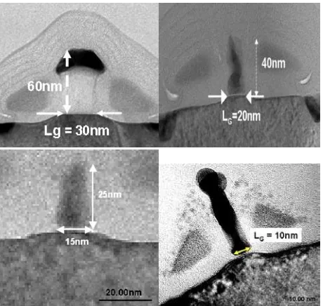
While the state-of-the-art logic products today utilize transistors with physical gate lengths ~70nm, research laboratories in industry and academia have already demonstrated experimental devices with LG < 30nm [3-7]. Figure 2 shows the TEM cross section of the 30nm, 20nm, 15nm and 10nm experimental Si transistors produced in our laboratory [3-5]. Both the physical LG and height of the polySi gate electrode have been scaled aggressively, as shown in Figure 2.
As illustrated in Figure 3, these experimental devices demonstrate the expected scaling trends of intrinsic
NMOS gate delay (measured using a CV/I metric). The data show that even the 10nm experimental device shows intrinsic gate delay of ~0.1ps despite that its design is far from optimal.
Figure 2: TEM cross-sections of the 30nm, 20nm, 15nm, and 10nm experimental devices produced in our laboratory. All the devices have SiO2 gate dielectrics.
1.E-02 1.E-01 1.E+00 1.E+01
0.001 0.01 0.1 1
LG (µm)
G
a
te
De
la
y (
p
s)
10nm 20nm 15nm
Figure 3: Gate delay vs. transistor physical gate length LG.
Improved intrinsic energy-delay product per transistor is another benefit of transistor scaling that has allowed logic technology to scale to such massive levels of integration. Figure 4 illustrates the intrinsic energy-delay product of both production and research transistors down to 10nm physical gate length. The data from 20, 15, and 10nm
experimental transistors match the projected trend which bodes well for device scaling up to early next decade.
0.E+00
Drain Voltage (V)
Dr
Figure 6: Family of Id-Vd curves for the 15nm research device.
1.E-08
Gate Voltage (V)
Id
(A
/¬
m)
`
Figure 4: Intrinsic energy-delay product vs. physical gate length for production and research devices.
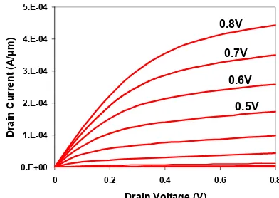
As devices are scaled, issues related to short channel control such as off-state leakage current, drain-induced-barrier-lowering (DIBL), and output conductance become increasingly important. Figures 5 and 6 show the subthreshold and family I-V characteristics respectively of the 15nm experimental device. The 15nm device shows reasonable short channel control with subthreshold slope = 95mV/decade, DIBL = 100mV/V and off-state leakage = 180nA/um at 0.8V power supply. However, as the transistor physical LG is scaled to 10nm, the subthreshold IV and output conductance characteristics show significant degradation, as shown in Figures 7 and 8. The experimental 10nm transistor shows poor short-channel control despite having intrinsic gate delay and energy-delay product that fall on the projected trends shown in figures 3 and 4.
Figure 7: Id-Vg characteristics at Vd=50mV and 0.75V for the 10nm experimental device.
0.E+00
Drain Voltage (V)
Dr
Gate Voltage (V)
Dr
S.S. = 95mV/decade DIBL = 100mV/V Ioff = 180nA/um
Gate Voltage (V)
Dr
S.S. = 95mV/decade DIBL = 100mV/V Ioff = 180nA/um 15nm NMOS
Figure 8: Family of Id-Vd curves for the 10nm research device.
The trend of continual increase in transistor off-state leakage with reducing physical LG is shown in Figure 9, for both production and research transistors. It is interesting to note that both production and research devices follow the same Ioff scaling trend. In order to control the power dissipation in future logic products, especially the ones that will use 10nm transistors, the off-state leakage trend needs to be slowed down. One potential solution is to use a fully-depleted silicon substrate to improve the short-channel performance such as subthreshold slope and DIBL.
Figure 5: Subthreshold characteristics of the experimental 15nm NMOS transistor.
Figure 9: Off-state leakage trend vs. transistor physical gate length.
Gate oxide leakage and alternative gate stacks
[
A
In addition to drain-to-source leakage, controlling gate dielectric leakage is an active area of device research. Figure 10 illustrates a TEM cross-section of a state-of-the-art SiO2 gate dielectric with a physical thickness of 0.8nm [8]. Continued improvement in device and short channel performance will require further gate oxide scaling below 0.8nm, which will require the use of an alternative gate dielectric stack, since SiO2 scaling is approaching its limit due to the increasing gate leakage with oxide scaling and the already-thin physical thickness. Figure 11 shows the gate dielectric leakage trend vs. equivalent oxide thickness for both SiO2 and a representative high-κ gate dielectric [8]. The use of high-κ gate dielectric reduces the gate oxide leakage significantly compared to SiO2 for the same EOT.
1.E-14
research data
1.E-06
Figure 11: Scaling trend of gate dielectric leakage (Jox) vs. equivalent
oxide thickness (EOT) [8].
0.0
Figure 12: Experimental CMOS devices with alternative gate dielectric stack [8].
New device architectures
Having identified off-state leakage as one of the scaling roadblocks, any future device architecture needs to address this issue. Several promising device architectures have been proposed to improve the scalability and leakage of transistors in upcoming generations, including single-gate fully depleted-substrate transistor (DST) [9], double-gate FINFET [10] and the fully-depleted tri-double-gate transistor [11], as shown in Figure 13. All three devices utilize a fully-depleted substrate and can be used to improve short-channel performance. Figure 14 shows the simulated subthreshold IV characteristics of a 30nm tri-gate NMOS. The 30nm device has excellent short channel performance with simulated subthreshold slope of 63mV/decade and DIBL of 70mV/V. In order to improve the total drive current for a given design space, the tri-gate devices can be connected in parallel with a common electrode as shown in Figure 15. The more silicon legs in a given design area, the higher the total drive current will be.
Figure 10: TEM cross-section of a 0.8nm SiO2 gate dielectric [8].
CMOS transistors with alternative gate dielectric stack has been demonstrated, as shown in Figure 12 [8]. These experimental devices use a high-κ/metal gate stack with EOT of 1.0nm and exhibit promising high-frequency device characteristics with Ft = 83GHz and Fmax = 35GHz for NMOS, and Ft = 41GHz and Fmax = 25GHz for PMOS. The use of alternative gate stack will be required to facilitate the continual scaling of silicon nano-transistors toward the 10nm regime.
Of the three fully-depleted device architectures shown in Figure 13, the tri-gate transistor has the least stringent silicon body thickness (Tsi) and width (Wsi) requirement and is the easiest to fabricate [11]. Figure 16 shows that for a given transistor physical gate length, the tri-gate device show much more relaxed TSi requirement than the
single-gate planar DST, and much more relaxed WSi requirement compared to the double-gate FINFET transistor.
0 20 40 60
Device Gate Length, Lg (nm)
Sil
Device Gate Length, Lg (nm)
Sil
Figure 16: Simulation results showing the silicon geometry requirements for planar DST, double-gate, and tri-gate devices. Tri-gate requirements are the most relaxed allowing for improved manufacturability.
Achieving fully-depleted operation in a manufacturable device will provide one avenue to improve performance while optimizing off-state leakage currents.
Figure 13: (a) planar DST, (b) double-gate, and (c) Tri-gate devices.
Vd = 0.05V
0.00 0.10 0.20 0.30 0.40 0.50
VGS (V)
0.00 0.10 0.20 0.30 0.40 0.50
VGS (V)
Based on projections, transistor physical LG will reach about 15nm before end of this decade, and 10nm early next decade. Research silicon nano-transistors with 15nm and 10nm physical LG have already been demonstrated with improved intrinsic gate delay and energy-delay product trends over devices with longer LG. However, the transistor off-state leakage increases with decreasing LG, and will need to be reduced in order to control power dissipation in future logic products. In particular, the 10nm device exhibits poor short-channel performance and very high transistor off-state leakage which need to be improved. In addition, gate oxide leakage is increasing with reducing thickness and SiO2 is running out of atoms for further scaling. The short-channel performance of future silicon transistors will be improved using new transistor architecture such as the fully-depleted Tri-gate transistor architecture and the gate oxide leakage will be reduced using alternative gate stacks.
Figure 14: simulated I-V of a 30nm Tri-gate device.
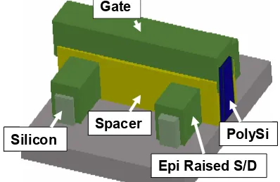
Gate
Silicon
Epi Raised S/D PolySi Spacer
Gate
Silicon
Epi Raised S/D PolySi Spacer
References:
[1] R. Chau et al., Nikkei Microdevices, p.83-88, Feb. 2002. [2] S. Thompson, IEDM, 2002, p. 61-64.
[3] R. Chau, 2001 Silicon Nanoelectronics, Kyoto, Japan, p.2-3. [4] B. Doyle et al., Intel Tech. Journal, vol. 6, no. 2, May 2002.
Figure 15: schematic of tri-gate devices showing multiple legs. [11] R. Chau et al., 2002 Int. Conf. on Solid State Devices & Materials, Nagoya, Japan, p.68-69.
![Figure 10: TEM cross-section of a 0.8nm SiO2 gate dielectric [8].](https://thumb-ap.123doks.com/thumbv2/123dok/1469866.1040882/3.612.94.285.362.532/figure-tem-cross-section-of-sio-gate-dielectric.webp)