IX. RANGKAIAN LOGIKA KOMBINASIONAL
A. PENDAHULUAN
- Suatu rangkaian diklasifkasikan sebagai kombinasional jika memiliki
sifat yaitu keluarannya ditentukan hanya oleh masukkan eksternal saja.
- Suatu rangkaian diklasifkasikan sequential jika ia memiliki sifat
Lanjutan…….
Rangkaian Logika
Kombinasional Sequential
Sinkron/Clock mode Asinkron
Rangkaian Logika
KOMBINASIONAL
Rangkaian Logika
Sequential Kombinasional
ENCODER DECODER
ADDER
MULTIPLEXER DE-MULTIPLEXER
SUBSTRACT COMPARATOR
HALF ADDER FULL ADDER
MODEL RANGKAIAN KOMBINASIONAL
Dengan :
F1 = F1 (I1, I2,…In ; t1 = F1 setelah t1 F2 = F2 (I1, I2,…In ; t2 = F2 setelah t2
- - -
Rangkaian Logika
Kombinasional (Komponen
tak ada Delay)
t1 t2
t n I1 I2 In F1 F2 Fn t1 t2
Lanjutan ……..
F ( kapital ) = Sinyal steady state dengan asumsi tidak ada delay.
t ( kecil ) = Sifat dinamis dari sinyal
yang dapat berubah selama
B. PROSEDUR PERANCANGAN
a. Pokok permasalahan sudah ditentukan yaitu jumlah input yang dibutuhkan serta jumlah output yang tertentu.
b. Susun kedalam tabel kebenaran (Truth Table).
C. DECODER
Decoder adalah rangkaian kombinasi yang akan memilih salah satu keluaran sesuai dengan
konfgurasi input. Decoder memiliki n input dan 2n output.
Blok Diagram Decoder.
Decoder
n to 2
n
IO I1
In
YO Y1
Contoh
Untuk Decoder 2 to 4
Decoder
n to 2
nIO Y
O
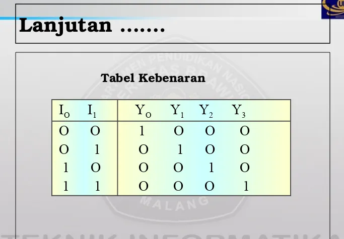
Lanjutan …….
Tabel Kebenaran
I
OI
1Y
OY
1Y
2Y
3O O
O 1
1 O
1 1
RANGKAIAN LOGIKA
I1
I0 Y
0
Y1
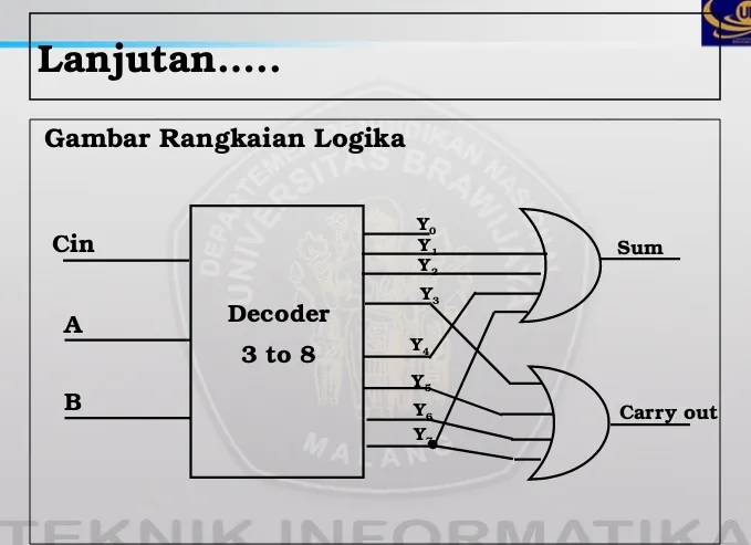
Untuk merancang rangkaian kombinasional dapat digunakan Decoder dan eksternal OR gate (rangkaian kombinasi n - input dan m– output dapat diimplementasikan dengan n to 2n line decoder dan m – OR gate).
Contoh.
Implementasikan suatu Full Adder dengan memakai Decoder dan 2 gerbang OR
Jawab :
Sum = A B Cin = Σ 1,2,4,7
Lanjutan…..
Gambar Rangkaian Logika
Decoder 3 to 8 Cin
A
B
Y1 Y0 Y2 Y3
Y4 Y5
CONTOH PERANCANGAN DECODER
Rancang BCD to Desimal Decoder untuk mengubah BCD ke seven segment ?
Catatan : Seven Segment. a
d
g b
c f
Another Code Converter Example:
BCD-to-Seven-Segment Converter
•
Seven-segment display:
–
7 LEDs (light emitting diodes), each one
controlled by an input
–
1 means “on”, 0 means “off”
–
Display digit “3”?
• Set a, b, c, d, g to 1
• Set e, f to 0
10/3 Chapter 3-ii: Combinational Logic Design (3.4 - 3.6)
d
14a
b
c
e
f
BCD-to-Seven-Segment
Converter
•
Input is a 4-bit BCD code
4 inputs (w, x,
y, z).
•
Output is a 7-bit code (a,b,c,d,e,f,g) that
allows for the decimal equivalent to be
displayed.
•
Example:
–
Input: 0000
BCD
–
Output: 1111110
(a=b=c=d=e=f=1, g=0)
10/3 1/18
15 Chapter 3-ii: Combinational Logic Design (3.4 - 3.6)
d
a
b
c
e
BCD-to-Seven-Segment (cont.)
Truth Table
Chapter 3-ii: Combinational 16
10/3
Digit wxyz abcdefg
0 0000 1111110
1 0001 0110000
2 0010 1101101
3 0011 1111001
4 0100 0110011
5 0101 1011011
6 0110 X011111
7 0111 11100X0
Digit wxyz abcdefg 8 1000 1111111
9 1001 111X011
D. ENCODER
Encoder adalah rangkaian kombinasi yang merupakan kebalikan dari Decoder yaitu manghasilkan output kode biner yang
berkorespondensi dengan nilai input. Encoder memiliki 2n input dan n output.
Tabel kebenaran Encoder 4 to 2
INPUT OUTPUT
I0 I1 I2 I3 X Y
1 0 0 0
0 1 0 0
0 0 1 0
0 0 0 1
0 0
0 1
1 0
1 1
X = I2 + I3
Encoders (cont.)
Chapter 3-ii: Combinational 18
Encoder Example
•
Example: 8-to-3 binary encoder (octal-to-binary)
Chapter 3-ii: Combinational
Logic Design (3.4 - 3.6) 19
10/3 1/18
A0 = D1 + D3 + D5 + D7
A1 = D2 + D3 + D6 + D7
Chapter 3-ii: Combinational 20
10/3
Simple Encoder Design Issues
•
There are two ambiguities associated with the
design of a simple encoder:
1. Only one input can be active at any given time. If two inputs are active simultaneously, the output
produces an undefined combination (for example, if
D3 and D6 are 1 simultaneously, the output of the
encoder will be 111.
2. An output with all 0's can be generated when all the
inputs are 0's,or when D0 is equal to 1.
Chapter 3-ii: Combinational
Logic Design (3.4 - 3.6) 21
Priority Encoders
•
Solves the ambiguities mentioned above.
•
Multiple asserted inputs are allowed; one
has priority over all others.
•
Separate indication of no asserted inputs.
Chapter 3-ii: Combinational 22
Chapter 3-ii: Combinational
Logic Design (3.4 - 3.6) 23
10/3 1/18
4-to-2 Priority Encoder (cont.)
•
The operation of the priority encoder is
such that:
•
If two or more inputs are equal to 1 at the
same time, the input in the
highest-numbered position will take precedence.
•
A
valid output indicator
, designated by
V, is set to 1 only when one or more inputs
are equal to 1. V = D
3+ D
2+ D
1+ D
0by
inspection.
Chapter 3-ii: Combinational 24
Chapter 3-ii: Combinational
Logic Design (3.4 - 3.6) 25
10/3 1/18
Chapter 3-ii: Combinational 26
10/3
A Matrix of switches = Keypad
Chapter 3-ii: Combinational
Logic Design (3.4 - 3.6) 27
10/3 1/18
C0 C1 C2 C3
R0
R1
R2
R3
Keypad Decoder IC - Encoder
Chapter 3-ii: Combinational 28
10/3
1 2 3 F
4 5 6 E
7 8 9 D
0 A B C
COL. 4-bit
ROW 4-bit
E. MULTIPLEXER ( MUX )
Blok Diagram Logika Mux.
Mux N x 1 0
1
n
A B
Input Data Output
PROSEDUR PERANCANGAN RANGKAIAN KOMBINASIONAL DENGAN MUX
1. Buat tabel kebenaran sesuai dengan kondisi input dan output serta nomor Mintermnya.
2. Salah satu variabel input digunakan sebagai Data dan sisanya dari variabel input sebagai address/selector.
3. Buat tabel Implementasi dan lingkari nomor Mintermnya yang sesuai dengan outputnya.
4. Jika 2 Mintermnya dalam satu kolom dilingkari, maka input Mux adalah 1 dan sebaliknya input Mux adalah berlogika 0
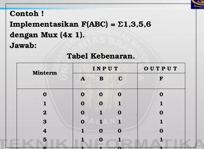
Contoh !
Implementasikan F(ABC) = Σ1,3,5,6 dengan Mux (4x 1).
Jawab:
Tabel Kebenaran.
Minterm I N P U T O U T P U T A B C F
0 1 2 3 4 5 6 7
0 0 0 0 0 1 0 1 0 0 1 1 1 0 0 1 0 1 1 1 0 1 1 1
Lanjutan………
Catatan.
Input Variabel A diambil sebagai data
sedangkan B dan C sebagai address.
Tabel Implementasi.
I
0I
1I
2I
3A
0
1
0
1
GAMBAR RANGKAIAN LOGIKA
Mux 4 X 1 I0
I1 I2 I3
B C
I
MUX implementation of
F(A,B,C) =
m(1,3,5,6)
Chapter 3-iii: Combinational 34
F.DEMULTIPLEXER (DEMUX)
Blok Diagram Logika DEMUX
DEMUX 1 x (n + 1) I
Input
Select/addressA B
Y0 Y1