527
CHAPTER
26
Balanced and
Bridged Amplifiers
B
alanced is beautiful–that’s what a mentor of mine told me many years ago. In this chapter three aspects of differential operation of power amplifiers will be dis-cussed. Single-ended power amplifiers that have balanced inputs will first be considered. These are the most common variant of differential operation in consumer audio. Most of these can also accommodate a single-ended input as well.Bridged amplifiers will next be discussed. These amplifiers are actually best referred to as bridge-connected amplifiers, as they are usually composed of a stereo pair of ampli-fiers that are fed the same signal but fed in opposite phase. Twice the voltage is available across their output terminals, so in this configuration they can supply four times the power into a given load impedance. Some of these amplifiers can be configured to accept balanced inputs as well.
Balanced amplifiers will finally be discussed. These are much like bridged amplifi-ers, and differences will be highlighted. In some cases, amplifiers that are called bal-anced amplifiers are merely what used to be called bridged amplifiers. The term balanced
is much more appealing than the term bridged.
26.1 Balanced Input Amplifiers
Most professional, and a number of hi-end audio power amplifiers incorporate bal-anced inputs using XLR connectors with pin 2 hot. This provides for improved rejection of external common mode noise.
Achieving balanced inputs for a single-ended (SE) power amplifier is not always straightforward, especially if the highest sound quality is to be maintained and if the amplifier must allow the user to operate the amplifier with either XLR balanced inputs or RCA single-ended inputs (with or without the need for a mode switch).
Gain and Input Impedance Considerations
Other important considerations include the gain of the amplifier in the two modes and the input impedance of the amplifier in the two modes. In particular, in the balanced input mode it is especially desirable that both the positive and negative inputs of the amplifier have the same input impedance so as to maintain the best possible common-mode rejection in the presence of finite driving impedances from the source.
amplifier. In high-end applications, it is sometimes frowned on to use an op-amp, which is the obvious and easy choice in implementing a balanced input capability.
Single and Triple Op-Amp Solutions
An op-amp can be used to implement a differential-to-single-ended converter, as shown in Figure 26.1a. Notice that this circuit presents different load impedance to single-ended sources on the positive and negative inputs. A single-single-ended source on the posi-tive input sees an input impedance of 20 kΩ. A single-ended source on the negaposi-tive input sees an input impedance of 10 kΩ. A common-mode source sees 20 kΩ on each side for a net of 10 kΩ. If the source impedance on both sides of the source is the same, common-mode rejection will be acceptable if resistor tolerances are tight.
In Figure 26.1b the resistor values are chosen so that the positive and negative inputs exhibit the same input impedance to a single-ended source (the resistors on the invert-ing side have been doubled to 20 kΩ). However, when a balanced signal is applied (with each of its signals referenced to ground at the source), the signal current flowing in the plus and minus inputs is not the same. Similarly, if a common-mode signal is applied to both inputs, the current flowing into the positive input is larger than the cur-rent flowing into the negative input. This happens because the virtual short at the op-amp inputs forces 1/2 of the voltage at the positive input to appear at the negative terminal of the op-amp. Because most balanced sources are symmetrically referenced to ground, this imbalance can cause undesired effects. If the positive and negative source impedances are not identical, common-mode rejection (CMRR) will suffer.
The single op-amp solution also forces a compromise between input impedance and noise. The circuit as shown has single-ended input impedances of only 20 kΩ and yet puts 20-kΩ resistors in the signal path, generating noise. The 20-kΩ input imped-ance also forces the use of large-value input-blocking capacitors if they are to be used. The three op-amp instrumentation amplifier shown in Figure 26.2 does not have these limitations. It can be used to achieve high common-mode rejection and symmetri-cal input impedances under all drive conditions. It also provides high input impedance while allowing the use of relatively low-value resistors in its implementation. However,
the circuit is more complex, and concerns about passing the signal through multiple op-amps are magnified.
The circuit is composed of unity-gain input buffers followed by a differential-SE converter with a gain of 1. Very high input impedances can be obtained by using low-noise JFET op-amps for the input buffers. The resistors surrounding the third op-amp should have 0.1% tolerance in order to maintain high CMRR.
Configuring the Power Amplifier as a Differential Amplifier
Another approach is to configure the main amplifier itself as a differential input ampli-fier in a way analogous to that of Figure 26.1a. This is illustrated in Figure 26.3a. Unfor-tunately, this results in relatively low input impedance on the inverting side because the
FIGURE 26.2 Triple op-amp instrumentation amplifier.
FIGURE 26.3 (a) Power amplifier configured as a differential amplifier. (b) With JFET input buffer on the
inverting input sides. The circuit can then be arranged so that the signal currents flowing in both buffers are made the same by equalizing the loading of the buffers. This will cause the buffers to act in a balanced, differential fashion, canceling out second harmonic distor-tion. Both of the differential inputs can have identical, high values of input impedance and both positive and negative signals encounter the same signal path for symmetry.
The discrete JFET input buffers must be run at fairly high currents to keep the distor-tion low, given the subsequent low impedances (on the order of 2.5k) that they must drive in the power amplifier’s differential-to-single-ended conversion input stage. This arrange-ment is illustrated in Figure 26.4. R7 makes the load seen by the positive-side buffer nom-inally the same as that seen by the negative-side buffer. This makes the power amplifier part of an instrumentation amplifier arrangement. The finite output impedance of the discrete JFET buffers can detract from common-mode rejection, however.
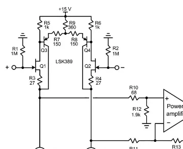
The Differential Complementary Feedback Quad (DCFQ)
The differential buffer shown in Figure 26.5 is referred to here as a differential comple-mentary feedback Quad (DCFQ). It employs two JFETs and two BJTs in a differential
arrangement analogous to a pair of JFET-bipolar CFPs. This circuit provides a low-distortion, low-impedance drive to the subsequent differential amplifier arrangement of the power amplifier.
JFETs Q1 and Q2 form a pair of source-followers that are helped by their respective complements Q3 and Q4. The BJTs are arranged as a differential pair, resulting in much-improved bias stability as compared to using two individual JFET-bipolar CFPs. R3 and R4 drop the source voltages down to 0 V to form the output signals.
THD of the DCFQ stage is less than 0.002% under all conditions of positive, nega-tive, and differential drive. This arrangement takes advantage of the good offset match-ing of the dual JFET, with pair-to-pair variations in Vgs resulting in only a common-mode offset that is ignored by the subsequent differential amplifier of the power amplifier. If desired, the common-mode level presented to the subsequent differential amplifier can be trimmed to zero with adjustment of R9. In principle, one could serve the currents in I1 and I2 to make the common-mode output DC level equal to zero.
26.2 Bridged Amplifiers
Bridged amplifiers are used widely where high power is required. This is especially so in the pro-sound arena. A simple bridged amplifier arrangement is illustrated in Figure 26.6. Two channels of a stereo amplifier are driven out of phase and the loud-speaker is connected across the hot outputs of the two amplifiers. A bridged power
amplifier can theoretically produce 4 times the power into a given load compared to its nonbridged counterpart (one channel of the stereo amplifier) using the same rail volt-ages. This is because the voltage across the loudspeaker is doubled and power goes as the square of voltage. Under these conditions, each of the two amplifiers “sees” an effective load resistance equal to half that of the loudspeaker impedance. For this rea-son, the bridged amplifier may produce somewhat less than 4 times the power.
Sound Quality
Bridged amplifiers have not always enjoyed a reputation for the highest-quality sound. This is partly because they are seeing half the impedance of the loudspeaker and the distortion of power amplifiers is virtually always higher when driving lower impedance loads. Moreover, the peak output current requirements are doubled, and some amplifiers may not be up to the task. Indeed, their protection circuits may be activating. Finally, bridged amplifiers are often abused. Each channel may not be rated to drive a 2-Ω load, but the amplifier may often be asked to drive a 4-Ω load in bridged mode.
Bridged amplifiers provide only half the damping factor into a given load because there are essentially two amplifier output impedances in series with the load. This can also detract from sound quality.
Power Supply Advantages
Amplifiers operating in bridged mode often enjoy some advantage in regard to the power supply. Single-ended amplifiers draw power from either the positive rail or the nega-tive rail on each half-cycle of the signal. This current flows through ground. The duty cycle of current flow from each rail is only 50%. In bridged-mode current is being drawn from both rails simultaneously and little or none of the output current flows through ground. Each rail is being used 100% of the time. The waveform of the current being sourced by each rail is full wave rather than half wave.
26.3 Balanced Amplifiers
Any amplifier that can accept balanced inputs and produce balanced outputs can be called a balanced amplifier. However, there are degrees of balance. A bridged amplifier with a balanced input can be called a balanced amplifier, and many so-called balanced amplifiers are made that way. For the audiophile, balanced is beautiful and bridged is brawn. That is why the term balanced is preferred when what would otherwise be a bridged amplifier is marketed to the audiophile community.
True Balanced Amplifiers
True balanced amplifiers comprise a single amplifier whose circuitry is balanced from input to output, not two separate amplifiers wired together in bridged mode. One ver-sion of an amplifier without negative feedback described in Chapter 25 was a truly balanced design. Indeed, in some ways it is easier to design a true balanced amplifier in the absence of negative feedback.
Building the differential open-loop amplifier is not difficult. It is fairly straightfor-ward to adopt a differential VAS arrangement and drive two copies of the output stage. Applying the negative feedback is where the added challenge lies.
Differential-Mode Feedback
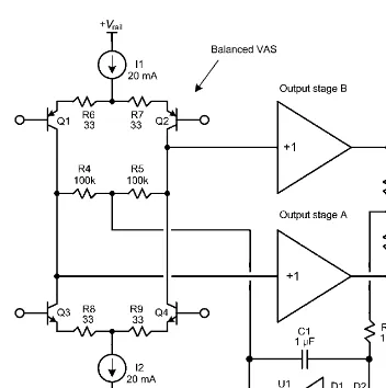
The output of a balanced amplifier is a differential (balanced) signal. The information applied to the loudspeaker is in the differential mode. That means the negative feed-back must be taken as the difference of the voltages existing across the two hot output terminals. The negative feedback must therefore be in the differential mode and be applied to the input circuits in the differential mode. One such arrangement is illus-trated in Figure 26.7. The amplifier is operated in the inverting shunt feedback configu-ration insofar as the feedback is concerned. The differential feedback creates a virtual short across the differential input terminals of the open-loop amplifier. Differential input signal current is applied to these input nodes through input resistors R1 and R2. The positive and negative halves of the balanced input signal are buffered so that the amplifier can present high impedance to the source. This differential buffering function can be implemented with the DCFQ differential buffer shown in Figure 26.5.
this reason a second feedback loop called a common-mode feedback loop is needed in most true balanced amplifiers to sense the output common-mode level and drive it to zero. However, if the differential inputs of the open-loop amplifier have high common-mode rejection, as desired, they will not be responsive to common-mode error signals fed back by the common-mode feedback. The common-mode feedback typically must be applied somewhere within the forward path of the amplifier. This feedback loop must
also obey stability criteria. However, this loop need not have high closed-loop band-width. In fact, this circuit can be just another DC servo.
Figure 26.9 shows a balanced amplifier with a common-mode DC servo. A simpli-fied version of a differential VAS is shown, and the two output stages are merely shown as gain blocks. The usual bias spreaders have been omitted for simplicity. The common-mode component of the output signal is derived by summing resistors R1 and R2 and applied to the integrator of the common-mode DC servo. The DC error signal from the servo is applied to VAS load resistors R4 and R5. If the common-mode output voltage is too high, the integrator output will go negative and pull both VAS output nodes in a negative direction to correct the error. Notice that the VAS load resistors are not unlike the load resistors employed in low-feedback amplifiers, but in this application they can have much higher values. Current sources I1 and I2 should be well matched in this approach so that the common-mode servo has adequate cor-rection range. In other IPS-VAS arrangements the common-mode corcor-rection signal can be applied to the input stage.