C h a p t e r
5
/ Imperfections in Solids
A
field ion micrograph taken at the tip of a pointed tungsten specimen. Field ion microscopy is a sophisticated and fascinating technique that permits observation of indivi-dual atoms in a solid, which are represented by white spots. The symmetry and regu-larity of the atom arrange-ments are evident from the positions of the spots in this micrograph. A disruption of this symmetry occurs along a grain boundary, which is traced by the arrows. Approximately 3,460,000ⴛ. (Photomicrograph courtesy of J. J. Hren andR. W . Newman.)
W hy Study
Imperfections in Solids?The properties of some materials are profoundly influenced by the presence of imperfections. Con-sequently, it is important to have a knowledge about the types of imperfections that exist, and the roles they play in affecting the behavior of materials. For example, the mechanical properties of pure metals experience significant alterations when alloyed (i.e., when impurity atoms are added)— e.g., sterling silver (92.5% silver- 7.5%
copper) is much harder and stronger than pure silver (Section 8.10).
Also, integrated circuit microelectronic devices found in our computers, calculators, and home appliances function because of highly controlled concentrations of specific impurities that are incorporated into small, localized regions of semiconducting materials (Sections 12.11兵and 12.14其).
L e a r n i n g O b j e c t i v e s
After stu d yin g th is ch a p ter you sh ou ld b e a b le to d o th e followin g:
1. Descr ib e b oth va ca n cy a n d self- in ter stitia l cr ys-ta llin e d efects.
2. Ca lcu la te th e eq u ilib r iu m n u m b er of va ca n cies in a m a ter ia l a t som e sp ecified tem p er a tu r e, given th e r eleva n t con sta n ts.
3. Na m e th e two typ es of solid solu tion s, a n d p r o-vid e a b r ief wr itten d efin ition a n d / or sch em a tic sk etch of ea ch .
4. Na m e a n d d escr ib e eigh t d iffer en t ion ic p oin t d e-fects th a t a r e fou n d in cer a m ic com p ou n d s. 5. Given th e m a sses a n d a tom ic weigh ts of two or
m or e elem en ts in a m eta l a lloy, ca lcu la te th e
5.1 I
NTRODUCTIONFor a crystalline solid we have tacitly assumed that perfect order exists throughout the material on an atomic scale. H owever, such an idealized solid does not exist; all contain large numbers of various defects or imperfections. A s a matter of fact, many of the properties of materials are profoundly sensitive to deviations from crystalline perfection; the influence is not always adverse, and often specific charac-teristics are deliberately fashioned by the introduction of controlled amounts or numbers of particular defects, as detailed in succeeding chapters.
By ‘‘crystalline defect’’ is meant a lattice irregularity having one or more of its dimensions on the order of an atomic diameter. Classification of crystalline imperfections is frequently made according to geometry or dimensionality of the defect. Several different imperfections are discussed in this chapter, including point defects (those associated with one or two atomic positions), linear (or one-dimen-sional) defects, as well as interfacial defects, or boundaries, which are two-dimen-sional. Impurities in solids are also discussed, since impurity atoms may exist as point defects.兵Finally, techniques for the microscopic examination of defects and the structure of materials are briefly described.其
P O I N T D E F E C T S
5.2 P
OINTD
EFECTS INM
ETALSThe simplest of the point defects is avacancy,or vacant lattice site, one normally occupied from which an atom is missing (Figure 5.1). A ll crystalline solids contain vacancies and, in fact, it is not possible to create such a material that is free of these defects. The necessity of the existence of vacancies is explained using principles of thermodynamics; in essence, the presence of vacancies increases the entropy (i.e., the randomness) of the crystal.
The equilibrium number of vacanciesNvfor a given quantity of material depends
on and increases with temperature according to
Nv⫽Nexp
冉
⫺Qv
k T
冊
(5.1)103
weigh t p er cen t a n d a tom ic p er cen t for ea ch el-em en t.6. For ea ch of ed ge, scr ew, a n d m ixed d isloca tion s: (a ) d escr ib e a n d m a k e a d r a win g of th e d
islo-ca tion ;
(b ) n ote th e loca tion of th e d isloca tion lin e; a n d (c) in d ica te th e d ir ection a lon g wh ich th e d
islo-ca tion lin e exten d s.
7. Descr ib e th e a tom ic str u ctu r e with in th e vicin ity of (a ) a gr a in b ou n d a r y, a n d (b ) a twin
In this expression,N is the total number of atomic sites,Qvis the energy required
for the formation of a vacancy,T is the absolute temperature1 in kelvins, and k is the gas or Boltzmann’s constant. The value ofk is 1.38 ⫻ 10⫺23 J /atom-K, or 8.62 ⫻ 10⫺5 eV /atom-K, depending on the units of Q
v.2 Thus, the number of
vacancies increases exponentially with temperature; that is, asT in E quation 5.1 increases, so does also the expression exp⫺(Qv/k T). For most metals, the fraction
of vacanciesNv/N just below the melting temperature is on the order of 10⫺4; that
is, one lattice site out of 10,000 will be empty. A s ensuing discussions indicate, a number of other material parameters have an exponential dependence on tempera-ture similar to that of E quation 5.1.
A self-interstitial is an atom from the crystal that is crowded into an interstitial site, a small void space that under ordinary circumstances is not occupied. This kind of defect is also represented in Figure 5.1. In metals, a self-interstitial introduces relatively large distortions in the surrounding lattice because the atom is substan-tially larger than the interstitial position in which it is situated. Consequently, the formation of this defect is not highly probable, and it exists in very small concentrations, which are significantly lower than for vacancies.
E
XAMP LEP
ROBLEM5.1
Calculate the equilibrium number of vacancies per cubic meter for copper at 1000⬚C. The energy for vacancy formation is 0.9 eV /atom; the atomic weight and density (at 1000⬚C) for copper are 63.5 g/mol and 8.40 g/cm3, respectively.
S
O L U T I O NThis problem may be solved by using E quation 5.1; it is first necessary, however, to determine the value of N, the number of atomic sites per cubic meter for 104 ● Ch a p ter 5 / Im p er fection s in Solid s
FIGURE5.1 Two-dimensional representations of a vacancy and a self-interstitial. (A dapted from W. G . Moffatt, G . W. Pearsall, and J. Wulff,T he Structure and Properties of M aterials,Vol. I,
Structure,p. 77. Copyright ©1964 by John Wiley & Sons, New York. R eprinted by permission of John Wiley & Sons, Inc.)
1A bsolute temperature in kelvins (K) is equal to⬚C⫹273.
5.3 P oin t Defects in Cer a m ics ● 105
copper, from its atomic weight ACu, its density, and A vogadro’s number NA, according to
N⫽NA
ACu (5.2)
⫽(6.023⫻10
23atoms/mol)(8.40 g/cm3)(106cm3/m3)
63.5 g/mol
⫽8.0⫻1028atoms/m3
Thus, the number of vacancies at 1000⬚C (1273 K) is equal to
Nv⫽N exp
冉
⫺Qv
kT
冊
⫽(8.0⫻1028atoms/m3) exp
冋
⫺ (0.9 eV)(8.62⫻10⫺5eV /K)(1273 K)
册
⫽2.2⫻1025vacancies/m35.3 P
OINTD
EFECTS INC
ERAMICSPoint defects also may exist in ceramic compounds. A s with metals, both vacancies and interstitials are possible; however, since ceramic materials contain ions of at least two kinds, defects for each ion type may occur. For example, in NaCl, Na interstitials and vacancies and Cl interstitials and vacancies may exist. It is highly improbable that there would be appreciable concentrations of anion (Cl⫺)
intersti-tials. The anion is relatively large, and to fit into a small interstitial position, substan-tial strains on the surrounding ions must be introduced. A nion and cation vacancies and a cation interstitial are represented in Figure 5.2.
The expression defect structure is often used to designate the types and concen-trations of atomic defects in ceramics. Because the atoms exist as charged ions, when defect structures are considered, conditions of electroneutrality must be maintained.
FIGURE5.2
E lectroneutrality is the state that exists when there are equal numbers of positive and negative charges from the ions. A s a consequence, defects in ceramics do not occur alone. O ne such type of defect involves a cation –vacancy and a cation – interstitial pair. This is called a Frenkel defect (Figure 5.3). It might be thought of as being formed by a cation leaving its normal position and moving into an interstitial site. There is no change in charge because the cation maintains the same positive charge as an interstitial.
A nother type of defect found in A X materials is a cation vacancy–anion vacancy pair known as a Schottky defect, also schematically diagrammed in Figure 5.3. This defect might be thought of as being created by removing one cation and one anion from the interior of the crystal and then placing them both at an external surface. Since both cations and anions have the same charge, and since for every anion vacancy there exists a cation vacancy, the charge neutrality of the crystal is main-tained.
The ratio of cations to anions is not altered by the formation of either a Frenkel or a Schottky defect. If no other defects are present, the material is said to be stoichiometric. Stoichiometry may be defined as a state for ionic compounds wherein there is the exact ratio of cations to anions as predicted by the chemical formula. For example, NaCl is stoichiometric if the ratio of Na⫹ions to Cl⫺ions is exactly
1 : 1. A ceramic compound is nonstoichiometric if there is any deviation from this exact ratio.
Nonstoichiometry may occur for some ceramic materials in which two valence (or ionic) states exist for one of the ion types. Iron oxide (wu¨stite, FeO ) is one such material, for the iron can be present in both Fe2⫹and Fe3⫹states; the number
of each of these ion types depends on temperature and the ambient oxygen pressure. The formation of an Fe3⫹ion disrupts the electroneutrality of the crystal by
introduc-ing an excess⫹1 charge, which must be offset by some type of defect. This may be accomplished by the formation of one Fe2⫹
vacancy (or the removal of two positive charges) for every two Fe3⫹
ions that are formed (Figure 5.4). The crystal is no longer stoichiometric because there is one more O ion than Fe ion; however, the crystal remains electrically neutral. This phenomenon is fairly common in iron oxide, and, in fact, its chemical formula is often written as Fe1⫺xO (where x is some 106 ● Ch a p ter 5 / l in Solid s
5.4 Im p u r ities in Solid s ● 107
small and variable fraction substantially less than unity) to indicate a condition of nonstoichiometry with a deficiency of Fe.
5.4 I
MPURITIES INS
OLIDSIMP URITIES IN METALS
A pure metal consisting of only one type of atom just isn’t possible; impurity or foreign atoms will always be present, and some will exist as crystalline point defects. In fact, even with relatively sophisticated techniques, it is difficult to refine metals to a purity in excess of 99.9999%. A t this level, on the order of 1022to 1023impurity atoms will be present in one cubic meter of material. Most familiar metals are not highly pure; rather, they are alloys, in which impurity atoms have been added intentionally to impart specific characteristics to the material. O rdinarily alloying is used in metals to improve mechanical strength and corrosion resistance. For example, sterling silver is a 92.5% silver –7.5% copper alloy. In normal ambient environments, pure silver is highly corrosion resistant, but also very soft. A lloying with copper enhances the mechanical strength significantly, without depreciating the corrosion resistance appreciably.
The addition of impurity atoms to a metal will result in the formation of a solid solution and /or a new second phase, depending on the kinds of impurity, their concentrations, and the temperature of the alloy. The present discussion is con-cerned with the notion of a solid solution; treatment of the formation of a new phase is deferred to Chapter 10.
Several terms relating to impurities and solid solutions deserve mention. With regard to alloys, solute and solvent are terms that are commonly employed. ‘‘Sol-vent’’ represents the element or compound that is present in the greatest amount; on occasion, solvent atoms are also called host atoms. ‘‘Solute’’ is used to denote an element or compound present in a minor concentration.
SOLID SOLUTIONS
A solid solution forms when, as the solute atoms are added to the host material, the crystal structure is maintained, and no new structures are formed. Perhaps it is useful to draw an analogy with a liquid solution. If two liquids, soluble in each other (such as water and alcohol) are combined, a liquid solution is produced as the molecules intermix, and its composition is homogeneous throughout. A solid solution is also compositionally homogeneous; the impurity atoms are randomly and uniformly dispersed within the solid.
FIGURE5.4 Schematic representation of an Fe2⫹
Impurity point defects are found in solid solutions, of which there are two types: substitutional and interstitial. For substitutional, solute or impurity atoms replace or substitute for the host atoms (Figure 5.5). There are several features of the solute and solvent atoms that determine the degree to which the former dissolves in the latter; these are as follows:
1. Atomic size factor. A ppreciable quantities of a solute may be accommo-dated in this type of solid solution only when the difference in atomic radii between the two atom types is less than about ⫾15%. O therwise the solute atoms will create substantial lattice distortions and a new phase will form.
2. Crystal structure. For appreciable solid solubility the crystal structures for metals of both atom types must be the same.
3. E lectronegativity. The more electropositive one element and the more electronegative the other, the greater is the likelihood that they will form an intermetallic compound instead of a substitutional solid solution. 4. Valences. O ther factors being equal, a metal will have more of a ten-dency to dissolve another metal of higher valency than one of a lower va-lency.
A n example of a substitutional solid solution is found for copper and nickel. These two elements are completely soluble in one another at all proportions. With regard to the aforementioned rules that govern degree of solubility, the atomic radii for copper and nickel are 0.128 and 0.125 nm, respectively, both have the FCC crystal structure, and their electronegativities are 1.9 and 1.8 (Figure 2.7); finally, the most common valences are ⫹1 for copper (although it sometimes can be ⫹2) and ⫹2 for nickel.
For interstitial solid solutions, impurity atoms fill the voids or interstices among the host atoms (see Figure 5.5). For metallic materials that have relatively high atomic packing factors, these interstitial positions are relatively small. Consequently, the atomic diameter of an interstitial impurity must be substantially smaller than that of the host atoms. Normally, the maximum allowable concentration of interstitial impurity atoms is low (less than 10%). E ven very small impurity atoms are ordinarily 108 ● Ch a p ter 5 / Im p er fection s in Solid s
5.4 Im p u r ities in Solid s ● 109
larger than the interstitial sites, and as a consequence they introduce some lattice strains on the adjacent host atoms. Problem 5.9 calls for determination of the radii of impurity atoms (in terms of R, the host atom radius) that will just fit into interstitial positions without introducing any lattice strains for both FCC and BCC crystal structures.
Carbon forms an interstitial solid solution when added to iron; the maximum concentration of carbon is about 2%. The atomic radius of the carbon atom is much less than that for iron: 0.071 nm versus 0.124 nm.
IMP URITIES IN CERAMICS
Impurity atoms can form solid solutions in ceramic materials much as they do in metals. Solid solutions of both substitutional and interstitial types are possible. For an interstitial, the ionic radius of the impurity must be relatively small in comparison to the anion. Since there are both anions and cations, a substitutional impurity will substitute for the host ion to which it is most similar in an electrical sense: if the impurity atom normally forms a cation in a ceramic material, it most probably will substitute for a host cation. For example, in sodium chloride, impurity Ca2⫹ and
O2⫺ions would most likely substitute for Na⫹and Cl⫺ions, respectively. Schematic
representations for cation and anion substitutional as well as interstitial impurities are shown in Figure 5.6. To achieve any appreciable solid solubility of substituting impurity atoms, the ionic size and charge must be very nearly the same as those of one of the host ions. For an impurity ion having a charge different from the host ion for which it substitutes, the crystal must compensate for this difference in charge so that electroneutrality is maintained with the solid. O ne way this is accomplished is by the formation of lattice defects—vacancies or interstitials of both ion types, as discussed above.
Interstitial impurity atom
Substitutional impurity ions
E
XAMP LEP
ROBLEM5.2
If electroneutrality is to be preserved, what point defects are possible in NaCl when a Ca2⫹
substitutes for an Na⫹
ion? H ow many of these defects exist for every Ca2⫹ion?
S
O L U T I O NR eplacement of an Na⫹ by a Ca2⫹ ion introduces one extra positive charge.
E lectroneutrality is maintained when either a single positive charge is eliminated or another single negative charge is added. R emoval of a positive charge is accomplished by the formation of one Na⫹vacancy. A lternatively, a Cl⫺
intersti-tial will supply an additional negative charge, negating the effect of each Ca2⫹
ion. H owever, as mentioned above, the formation of this defect is highly un-likely.
5.5 P
OINTD
EFECTS INP
OLYMERSIt should be noted that the defect concept is different in polymers (than in metals and ceramics) as a consequence of the chainlike macromolecules and the nature of the crystalline state for polymers. Point defects similar to those found in metals have been observed in crystalline regions of polymeric materials; these include vacancies and interstitial atoms and ions. Chain ends are considered to be defects inasmuch as they are chemically dissimilar to normal chain units; vacancies are also associated with the chain ends. Impurity atoms/ions or groups of atoms/ions may be incorporated in the molecular structure as interstitials; they may also be associ-ated with main chains or as short side branches.
5.6 S
P ECIFICATION OFC
OMP OSITIONIt is often necessary to express the composition (or concentration )3of an alloy in terms of its constituent elements. The two most common ways to specify composition are weight (or mass) percent and atom percent. The basis for weight percent (wt%) is the weight of a particular element relative to the total alloy weight. For an alloy that contains two hypothetical atoms denoted by 1 and 2, the concentration of 1 in wt%, C1, is defined as
C1⫽ m1 m1⫹m2
⫻100 (5.3)
where m1and m2represent the weight (or mass) of elements 1 and 2, respectively. The concentration of 2 would be computed in an analogous manner.
The basis for atom percent (at%) calculations is the number of moles of an element in relation to the total moles of the elements in the alloy. The number of moles in some specified mass of a hypothetical element 1, nm 1, may be computed 110 ● Ch a p ter 5 / Im p er fection s in Solid s
5.7 Disloca tion s—Lin ea r Defects ● 111
as follows:
nm 1⫽ m⬘1
A1
(5.4)
H ere, m⬘1and A1denote the mass (in grams) and atomic weight, respectively, for element 1.
Concentration in terms of atom percent of element 1 in an alloy containing 1 and 2 atoms, C⬘1, is defined by4
C⬘1⫽ nm 1 nm 1⫹nm 2
⫻100 (5.5)
In like manner, the atom percent of 2 may be determined.
A tom percent computations also can be carried out on the basis of the number of atoms instead of moles, since one mole of all substances contains the same number of atoms.
COMP OSITION CONVERSIONS (CD- ROM)
M I S C E L L A N E O U S I M P E R F E C T I O N S
5.7 D
ISLOCATIONS—L
INEARD
EFECTSA dislocation is a linear or one-dimensional defect around which some of the atoms are misaligned. O ne type of dislocation is represented in Figure 5.7: an extra portion
Edge dislocation
line
Burgers vector b
FIGURE5.7 The atom positions around an edge dislocation; extra half-plane of atoms shown in perspective. (A dapted from A . G . G uy, E ssentials of Materials Science, McG raw-H ill Book Company, New York, 1976, p. 153.)
of a plane of atoms, or half-plane, the edge of which terminates within the crystal. This is termed anedge dislocation; it is a linear defect that centers around the line that is defined along the end of the extra half-plane of atoms. This is sometimes termed thedislocation line,which, for the edge dislocation in Figure 5.7, is perpen-dicular to the plane of the page. Within the region around the dislocation line there is some localized lattice distortion. The atoms above the dislocation line in Figure 5.7 are squeezed together, and those below are pulled apart; this is reflected in the slight curvature for the vertical planes of atoms as they bend around this extra half-plane. The magnitude of this distortion decreases with distance away from the dislocation line; at positions far removed, the crystal lattice is virtually perfect. Sometimes the edge dislocation in Figure 5.7 is represented by the symbol⬜, which also indicates the position of the dislocation line. A n edge dislocation may also be formed by an extra half-plane of atoms that is included in the bottom portion of the crystal; its designation is a ⬜ .
A nother type of dislocation, called a screw dislocation, exists, which may be thought of as being formed by a shear stress that is applied to produce the distortion shown in Figure 5.8a: the upper front region of the crystal is shifted one atomic distance to the right relative to the bottom portion. The atomic distortion associated with a screw dislocation is also linear and along a dislocation line, lineA Bin Figure 5.8b. The screw dislocation derives its name from the spiral or helical path or ramp that is traced around the dislocation line by the atomic planes of atoms. Sometimes the symbol is used to designate a screw dislocation.
Most dislocations found in crystalline materials are probably neither pure edge nor pure screw, but exhibit components of both types; these are termed mixed dislocations.A ll three dislocation types are represented schematically in Figure 5.9; the lattice distortion that is produced away from the two faces is mixed, having varying degrees of screw and edge character.
The magnitude and direction of the lattice distortion associated with a disloca-tion is expressed in terms of a Burgers vector, denoted by a b. Burgers vectors are indicated in Figures 5.7 and 5.8 for edge and screw dislocations, respectively. Furthermore, the nature of a dislocation (i.e., edge, screw, or mixed) is defined by the relative orientations of dislocation line and Burgers vector. For an edge, they are perpendicular (Figure 5.7), whereas for a screw, they are parallel (Figure 5.8); they are neither perpendicular nor parallel for a mixed dislocation. A lso, even though a dislocation changes direction and nature within a crystal (e.g., from edge to mixed to screw), the Burgers vector will be the same at all points along its line. For example, all positions of the curved dislocation in Figure 5.9 will have the Burgers vector shown. For metallic materials, the Burgers vector for a dislocation will point in a close-packed crystallographic direction and will be of magnitude equal to the interatomic spacing.
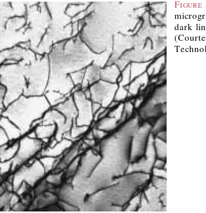
D islocations can be observed in crystalline materials using electron-microscopic techniques. In Figure 5.10, a high-magnification transmission electron micrograph, the dark lines are the dislocations.
Virtually all crystalline materials contain some dislocations that were introduced during solidification, during plastic deformation, and as a consequence of thermal stresses that result from rapid cooling. D islocations are involved in the plastic deformation of these materials, as discussed in Chapter 8. D islocations have been observed in polymeric materials; however, some controversy exists as to the nature of dislocation structures in polymers and the mechanism(s) by which polymers plastically deform.
5.7 Dislocations— Linear Defects ● 113
Dislocation line
Burgers vector b
D
C
(a)
A B
C D
(b) A
b
FIGURE5.8 (a) A
(a)
(b)
b
b
B
C A
B
b
b
A
C
b 114 ● Ch a p ter 5 / Im p er fection s in Solid s
5.8 In ter fa cia l Defects ● 115
5.8 I
NTERFACIALD
EFECTSInterfacial defects are boundaries that have two dimensions and normally separate regions of the materials that have different crystal structures and /or crystallographic orientations. These imperfections include external surfaces, grain boundaries, twin boundaries, stacking faults, and phase boundaries.
EXTERNAL SURFACES
O ne of the most obvious boundaries is the external surface, along which the crystal structure terminates. Surface atoms are not bonded to the maximum number of nearest neighbors, and are therefore in a higher energy state than the atoms at interior positions. The bonds of these surface atoms that are not satisfied give rise to a surface energy, expressed in units of energy per unit area (J /m2 or erg/cm2). To reduce this energy, materials tend to minimize, if at all possible, the total surface area. For example, liquids assume a shape having a minimum area —the droplets become spherical. O f course, this is not possible with solids, which are mechani-cally rigid.
GRAIN BOUNDARIES
A nother interfacial defect, the grain boundary, was introduced in Section 3.17 as the boundary separating two small grains or crystals having different crystallographic orientations in polycrystalline materials. A grain boundary is represented schemati-cally from an atomic perspective in Figure 5.11. Within the boundary region, which is probably just several atom distances wide, there is some atomic mismatch in a transition from the crystalline orientation of one grain to that of an adjacent one. Various degrees of crystallographic misalignment between adjacent grains are possible (Figure 5.11). When this orientation mismatch is slight, on the order of a few degrees, then the term small- (or low-) angle grain boundary is used. These boundaries can be described in terms of dislocation arrays. O ne simple small-angle grain boundary is formed when edge dislocations are aligned in the manner of Figure 5.12. This type is called a tilt boundary; the angle of misorientation, , is
also indicated in the figure. When the angle of misorientation is parallel to the boundary, a twist boundary results, which can be described by an array of screw dislo-cations.
The atoms are bonded less regularly along a grain boundary (e.g., bond angles are longer), and consequently, there is an interfacial or grain boundary energy 116 ● Ch a p ter 5 / Im p er fection s in Solid s
Angle of misalignment Angle of misalignment
Low-angle grain boundary
High-angle grain boundary
FIGURE5.11 Schematic diagram showing low-and high-angle grain boundaries and the adjacent atom positions.
FIGURE5.12 D emonstration of how a tilt boundary having an angle of misorientationresults from an alignment of edge dislocations.
5.8 In ter fa cia l Defects ● 117
similar to the surface energy described above. The magnitude of this energy is a function of the degree of misorientation, being larger for high-angle boundaries. G rain boundaries are more chemically reactive than the grains themselves as a consequence of this boundary energy. Furthermore, impurity atoms often preferen-tially segregate along these boundaries because of their higher energy state. The total interfacial energy is lower in large or coarse-grained materials than in fine-grained ones, since there is less total boundary area in the former. G rains grow at elevated temperatures to reduce the total boundary energy, a phenomenon ex-plained in Section 8.14.
In spite of this disordered arrangement of atoms and lack of regular bond-ing along grain boundaries, a polycrystalline material is still very strong; cohesive forces within and across the boundary are present. Furthermore, the density of a polycrystalline specimen is virtually identical to that of a single crystal of the same material.
TWIN BOUNDARIES
A twin boundary is a special type of grain boundary across which there is a specific mirror lattice symmetry; that is, atoms on one side of the boundary are located in mirror image positions of the atoms on the other side (Figure 5.13). The region of material between these boundaries is appropriately termed a twin. Twins result from atomic displacements that are produced from applied mechanical shear forces (mechanical twins), and also during annealing heat treatments following deforma-tion (annealing twins). Twinning occurs on a definite crystallographic plane and in a specific direction, both of which depend on the crystal structure. A nnealing twins are typically found in metals that have the FCC crystal structure, while mechanical twins are observed in BCC and H CP metals.兵The role of mechanical twins in the deformation process is discussed in Section 8.8. A nnealing twins may be observed in the photomicrograph of the polycrystalline brass specimen shown in Figure 5.15c. The twins correspond to those regions having relatively straight and parallel sides and a different visual contrast than the untwinned regions of the grains within which they reside. A n explanation for the variety of textural contrasts in this photomicrograph is provided in Section 5.12.其
MISCELLANEOUS INTERFACIAL DEFECTS
O ther possible interfacial defects include stacking faults, phase boundaries, and ferromagnetic domain walls. Stacking faults are found in FCC metals when there is an interruption in the ABCABCABC . . . stacking sequence of close-packed planes (Section 3.15). Phase boundaries exist in multiphase materials (Section 10.3)
across which there is a sudden change in physical and /or chemical characteristics. 兵For ferromagnetic and ferrimagnetic materials, the boundary that separates regions having different directions of magnetization is termed a domain wall, which is discussed in Section 18.7.其
With regard to polymeric materials, the surfaces of chain-folded layers (Figure 4.14) are considered to be interfacial defects, as are boundaries between two adjacent crystalline regions.
A ssociated with each of the defects discussed in this section is an interfacial energy, the magnitude of which depends on boundary type, and which will vary from material to material. Normally, the interfacial energy will be greatest for external surfaces and least for domain walls.
5.9 B
ULK ORV
OLUMED
EFECTSO ther defects exist in all solid materials that are much larger than those heretofore discussed. These include pores, cracks, foreign inclusions, and other phases. They are normally introduced during processing and fabrication steps. Some of these defects and their effects on the properties of materials are discussed in subse-quent chapters.
5.10 A
TOMICV
IBRATIONSE very atom in a solid material is vibrating very rapidly about its lattice position within the crystal. In a sense, these vibrations may be thought of as imperfections or defects. A t any instant of time not all atoms vibrate at the same frequency and amplitude, nor with the same energy. A t a given temperature there will exist a distribution of energies for the constituent atoms about an average energy. O ver time the vibrational energy of any specific atom will also vary in a random manner. With rising temperature, this average energy increases, and, in fact, the temperature of a solid is really just a measure of the average vibrational activity of atoms and molecules. A t room temperature, a typical vibrational frequency is on the order of 1013vibrations per second, whereas the amplitude is a few thousandths of a nano-meter.
Many properties and processes in solids are manifestations of this vibrational atomic motion. For example, melting occurs when the vibrations are vigorous enough to rupture large numbers of atomic bonds.兵A more detailed discussion of atomic vibrations and their influence on the properties of materials is presented in Chapter 17.其
M I C R O S C O P I C E X A M I N A T I O N
5.11 G
ENERAL5.13 Gr a in Size Deter m in a tion ● 119
grains are of microscopic dimensions, having diameters that may be on the order of microns,5and their details must be investigated using some type of microscope. G rain size and shape are only two features of what is termed the microstructure; these and other microstructural characteristics are discussed in subsequent chapters. O ptical, electron, and scanning probe microscopes are commonly used in mi-croscopy. These instruments aid in investigations of the microstructural features of all material types. Some of these techniques employ photographic equipment in conjunction with the microscope; the photograph on which the image is recorded is called a photomicrograph. In addition, some microstructural images are computer generated and /or enhanced.
Microscopic examination is an extremely useful tool in the study and character-ization of materials. Several important applications of microstructural examinations are as follows: to ensure that the associations between the properties and structure (and defects) are properly understood; to predict the properties of materials once these relationships have been established; to design alloys with new property combi-nations; to determine whether or not a material has been correctly heat treated; and to ascertain the mode of mechanical fracture. 兵Several techniques that are commonly used in such investigations are discussed next.其
5.12 M
ICROSCOPICT
ECHNIQUES(CD-ROM)
5.13 G
RAINS
IZED
ETERMINATIONThe grain size is often determined when the properties of a polycrystalline material are under consideration. In this regard, there exist a number of techniques by which size is specified in terms of average grain volume, diameter, or area. G rain size may be estimated by using an intercept method, described as follows. Straight lines all the same length are drawn through several photomicrographs that show the
FIGURE5.14 H igh-purity polycrystalline lead ingot in which the individual grains may be discerned. 0.7⫻. (R eproduced with permission from Metals H andbook, Vol. 9, 9th edition, Metallography and Microstructures, A merican Society for Metals, Metals Park, O H , 1985.)
5A micron (
grain structure. The grains intersected by each line segment are counted; the line length is then divided by an average of the number of grains intersected, taken over all the line segments. The average grain diameter is found by dividing this result by the linear magnification of the photomicrographs.
Probably the most common method utilized, however, is that devised by the A merican Society for Testing and Materials (A STM).6 The A STM has prepared several standard comparison charts, all having different average grain sizes. To each is assigned a number ranging from 1 to 10, which is termed the grain siz e num ber;the larger this number, the smaller the grains. A specimen must be properly prepared to reveal the grain structure, which is photographed at a magnification of 100⫻. G rain size is expressed as the grain size number of the chart that most nearly matches the grains in the micrograph. Thus, a relatively simple and convenient visual determination of grain size number is possible. G rain size number is used extensively in the specification of steels.
The rationale behind the assignment of the grain size number to these various charts is as follows. Let n represent the grain size number, and N the average number of grains per square inch at a magnification of 100⫻. These two parameters are related to each other through the expression
N⫽2n⫺1 (5.16)
S U M M A R Y
A ll solid materials contain large numbers of imperfections or deviations from crystal-line perfection. The several types of imperfection are categorized on the basis of their geometry and size. Point defects are those associated with one or two atomic positions; in metals these include vacancies (or vacant lattice sites), self-interstitials (host atoms that occupy interstitial sites), and impurity atoms.
With regard to atomic point defects in ceramics, interstitials and vacancies for each anion and cation type are possible. These imperfections often occur in pairs as Frenkel and Schottky defects to ensure that crystal electroneutrality is maintained. A solid solution may form when impurity atoms are added to a solid, in which case the original crystal structure is retained and no new phases are formed. For substitutional solid solutions, impurity atoms substitute for host atoms, and apprecia-ble solubility is possiapprecia-ble only when atomic diameters and electronegativities for both atom types are similar, when both elements have the same crystal structure, and when the impurity atoms have a valence that is the same as or less than the host material. Interstitial solid solutions form for relatively small impurity atoms that occupy interstitial sites among the host atoms.
For ceramic materials, the addition of impurity atoms may result in the forma-tion of substituforma-tional or interstitial solid soluforma-tions. A ny charge imbalance created by the impurity ions may be compensated by the generation of host ion vacancies or interstitials.
Composition of an alloy may be specified in weight percent or atom percent. The basis for weight percent computations is the weight (or mass) of each alloy constituent relative to the total alloy weight. A tom percents are calculated in terms of the number of moles for each constituent relative to the total moles of all the
120 ● Chapter 5 / Imperfections in Solids
References ● 121
elements in the alloy.兵E quations were provided for the conversion of one composi-tion scheme to another.其
D islocations are one-dimensional crystalline defects of which there are two pure types: edge and screw. A n edge may be thought of in terms of the lattice distortion along the end of an extra half-plane of atoms; a screw, as a helical planar ramp. For mixed dislocations, components of both pure edge and screw are found. The magnitude and direction of lattice distortion associated with a dislocation is specified by its Burgers vector. The relative orientations of Burgers vector and dislocation line are (1) perpendicular for edge, (2) parallel for screw, and (3) neither perpendicular nor parallel for mixed.
O ther imperfections include interfacial defects [external surfaces, grain bound-aries (both small- and high-angle), twin boundbound-aries, etc.], volume defects (cracks, pores, etc.), and atomic vibrations. E ach type of imperfection has some influence on the properties of a material.
Many of the important defects and structural elements of materials are of microscopic dimensions, and observation is possible only with the aid of a micro-scope.兵Both optical and electron microscopes are employed, usually in conjunction with photographic equipment. Transmissive and reflective modes are possible for each microscope type; preference is dictated by the nature of the specimen as well as the structural element or defect to be examined.其
兵More recent scanning probe microscopic techniques have been developed that generate topographical maps representing the surface features and characteristics of the specimen. E xaminations on the atomic and molecular levels are possible using these techniques.其
G rain size of polycrystalline materials is frequently determined using photomi-crographic techniques. Two methods are commonly employed: intercept and stan-dard comparison charts.
ASM H andbook, Vol. 9, Metallography and Micro-structures, A SM International, Materials Park, O H , 1985.
122 ● Chapter 5 / Imperfections in Solids
Chiang, Y. M., D . P. Birnie, III, and W. D . Kingery, P hysical Ceramics: P rinciples for Ceramic Sci-ence and E ngineering, John Wiley & Sons, Inc., New York, 1997.
Kingery, W. D ., H . K. Bowen, and D . R . U hlmann, Introduction to Ceramics, 2nd edition, John Wiley & Sons, New York, 1976. Chapters 4 and 5.
Moffatt, W. G ., G . W. Pearsall, and J. Wulff, The Structure and P roperties of Materials, Vol. 1, Structure, John Wiley & Sons, New York, 1964.
Phillips, V. A ., Modern Metallographic Techniques and Their Applications, Wiley-Interscience, New York, 1971.
Van Bueren, H . G ., Imperfections in Crystals, North-H olland Publishing Co., A msterdam (Wiley-Interscience, New York), 1960. Vander Voort, G . F., Metallography, P rinciples and
P ractice, McG raw-H ill Book Co., New York, 1984.
Q U E S T I O N S A N D P R O B L E M S
Note: To solve those problems having an asterisk (*) by their numbers, consultation of supplementary topics [appearing only on the CD -ROM (and not in print)] will probably be necessary.
5.1 Calculate the fraction of atom sites that are vacant for lead at its melting temperature of 327⬚C (600⬚F). A ssume an energy for va-cancy formation of 0.55 eV /atom.
5.2 Calculate the number of vacancies per cubic meter in iron at 850⬚C. The energy for va-cancy formation is 1.08 eV /atom. Further-more, the density and atomic weight for Fe are 7.65 g/cm3and 55.85 g/mol, respectively.
5.3 Calculate the energy for vacancy formation in silver, given that the equilibrium number of vacancies at 800⬚C (1073 K) is 3.6⫻1023 m⫺3. The atomic weight and density (at 800⬚C) for silver are, respectively, 107.9 g/ mol and 9.5 g/cm3.
5.4 Calculate the number of atoms per cubic me-ter in aluminum.
5.5 Would you expect Frenkel defects for anions to exist in ionic ceramics in relatively large concentrations? Why or why not?
5.6 In your own words, briefly define the term ‘‘stoichiometric.’’
5.7 If cupric oxide (CuO ) is exposed to reducing atmospheres at elevated temperatures, some of the Cu2⫹ions will become Cu⫹.
(a) U nder these conditions, name one crys-talline defect that you would expect to form in order to maintain charge neutrality. (b) H ow many Cu⫹
ions are required for the creation of each defect?
(c) H ow would you express the chemical formula for this nonstoichiometric material?
5.8 Below, atomic radius, crystal structure, elec-tronegativity, and the most common valence are tabulated, for several elements; for those that are nonmetals, only atomic radii are in-dicated.
Atomic Electro-Radius Cry stal
nega-Element (nm) Structure tivity Valence
Cu 0.1278 FCC 1.9 ⫹2
Which of these elements would you expect to form the following with copper:
(a) A substitutional solid solution having complete solubility?
(b) A substitutional solid solution of incom-plete solubility?
Qu estion s a n d P r ob lem s ● 123
5.9 For both FCC and BCC crystal structures, there are two different types of interstitial sites. In each case, one site is larger than the other, which site is normally occupied by impurity atoms. For FCC, this larger one is located at the center of each edge of the unit cell; it is termed an octahedral interstitial site. O n the other hand, with BCC the larger site type is found at 0,,positions—that is, lying on 兵100其 faces, and situated midway between two unit cell edges on this face and one-quarter of the distance between the other two unit cell edges; it is termed a tetra-hedral interstitial site. For both FCC and BCC crystal structures, compute the radius r of an impurity atom that will just fit into one of these sites in terms of the atomic radius R of the host atom.
5.10 (a) Suppose that Li2O is added as an impu-rity to CaO . If the Li⫹
substitutes for Ca2⫹
, what kind of vacancies would you expect to form? H ow many of these vacancies are created for every Li⫹added?
(b) Suppose that CaCl2is added as an impu-rity to CaO . If the Cl⫺
substitutes for O2⫺
, what kind of vacancies would you expect to form? H ow many of the vacancies are cre-ated for every Cl⫺
added?
5.11 What point defects are possible for MgO as an impurity in A l2O3? H ow many Mg2⫹ions must be added to form each of these defects?
5.12 What is the composition, in atom percent, of an alloy that consists of 30 wt% Z n and 70 wt% Cu?
5.13 What is the composition, in weight percent, of an alloy that consists of 6 at% Pb and 94 at% Sn?
5.14 Calculate the composition, in weight per-cent, of an alloy that contains 218.0 kg tita-nium, 14.6 kg of aluminum, and 9.7 kg of va-nadium.
5.15 What is the composition, in atom percent, of an alloy that contains 98 g tin and 65 g of lead?
5.16 What is the composition, in atom percent, of an alloy that contains 99.7 lbmcopper, 102 lbmzinc, and 2.1 lbmlead?
5.17* D erive the following equations: (a) E quation 5.7a.
(b) E quation 5.9a. (c) E quation 5.10a. (d) E quation 5.11b.
5.18* What is the composition, in atom percent, of an alloy that consists of 97 wt% Fe and 3 wt% Si?
5.19* Convert the atom percent composition in Problem 5.16 to weight percent.
5.20* The concentration of carbon in an iron-car-bon alloy is 0.15 wt%. What is the concentra-tion in kilograms of carbon per cubic meter of alloy?
5.21* D etermine the approximate density of a high-leaded brass that has a composition of 64.5 wt% Cu, 33.5 wt% Z n, and 2 wt% Pb.
5.22* For a solid solution consisting of two ele-ments (designated as 1 and 2), sometimes it is desirable to determine the number of atoms per cubic centimeter of one element in a solid solution, N1, given the concentra-tion of that element specified in weight per-cent, C1. This computation is possible using the following expression: A1⫽the atomic weight of element 1
D erive E quation 5.17 using E quation 5.2 and expressions contained in Section 5.3.
5.23 G old forms a substitutional solid solution with silver. Compute the number of gold atoms per cubic centimeter for a silver-gold alloy that contains 10 wt% A u and 90 wt% A g. The densities of pure gold and silver are 19.32 and 10.49 g/cm3, respectively.
124 ● Ch a p ter 5 / Im p er fection s in Solid s
a germanium-silicon alloy that contains 15 wt% G e and 85 wt% Si. The densities of pure germanium and silicon are 5.32 and 2.33 g/ cm3, respectively.
5.25* Sometimes it is desirable to be able to deter-mine the weight percent of one element, C1, that will produce a specified concentration in terms of the number of atoms per cubic centimeter, N1, for an alloy composed of two types of atoms. This computation is possible using the following expression:
D erive E quation 5.18 using E quation 5.2 and expressions contained in Section 5.3.
5.26 Molybdenum forms a substitutional solid so-lution with tungsten. Compute the weight percent of molybdenum that must be added to tungsten to yield an alloy that contains 1.0 ⫻ 1022Mo atoms per cubic centimeter. The densities of pure Mo and W are 10.22 and 19.30 g/cm3, respectively.
5.27 Niobium forms a substitutional solid solution with vanadium. Compute the weight percent of niobium that must be added to vanadium to yield an alloy that contains 1.55 ⫻ 1022 Nb atoms per cubic centimeter. The densities of pure Nb and V are 8.57 and 6.10 g/cm3, re-spectively.
5.28 Copper and platinum both have the FCC crystal structure and Cu forms a substitu-tional solid solution for concentrations up to approximately 6 wt% Cu at room tempera-ture. Compute the unit cell edge length for a 95 wt% Pt-5 wt% Cu alloy.
5.29 Cite the relative Burgers vector –dislocation line orientations for edge, screw, and mixed dislocations.
5.30 For both FCC and BCC crystal structures, the Burgers vector b may be expressed as
b⫽a
2[hkl ]
where a is the unit cell edge length and [hkl ] is the crystallographic direction having the greatest linear atomic density.
(a) What are the Burgers vector representa-tions for FCC, BCC, and simple cubic crystal structures? See Problems 3.70 and 3.71 at the end of Chapter 3.
(b) If the magnitude of the Burgers vector 兩b兩is
兩b兩⫽a
2(h
2⫹k2⫹l2)1/2
determine the values of兩b兩for aluminum and tungsten. You may want to consult Table 3.1.
5.31 (a) The surface energy of a single crystal depends on the crystallographic orientation with respect to the surface. E xplain why this is so.
(b) For an FCC crystal, such as aluminum, would you expect the surface energy for a (100) plane to be greater or less than that for a (111) plane? Why?
5.32 (a) For a given material, would you expect the surface energy to be greater than, the same as, or less than the grain boundary en-ergy? Why?
(b) The grain boundary energy of a low-angle grain boundary is less than for a high-angle one. Why is this so?
5.33 (a) Briefly describe a twin and a twin bound-ary.
(b) Cite the difference between mechanical and annealing twins.
5.34 For each of the following stacking sequences found in FCC metals, cite the type of planar defect that exists:
(a) . . . A B C A B C B A C B A . . . (b) . . . A B C A B C B C A B C . . . Now, copy the stacking sequences and indi-cate the position(s) of planar defect(s) with a vertical dashed line.
spec-Qu estion s a n d P r ob lem s ● 125
imen whose microstructure is shown in Fig-ure 5.16b; assume that the magnification is 100⫻, and use at least seven straight-line seg-ments.
5.36 E mploying the intercept technique, deter-mine the average grain size for the steel spec-imen whose microstructure is shown in Fig-ure 10.27a; use at least seven straight-line segments.
5.37* (a) For an A STM grain size of 4, approxi-mately how many grains would there be per square inch in a micrograph taken at a mag-nification of 100⫻?
(b) E stimate the grain size number for the photomicrograph in Figure 5.16b, assuming a magnification of 100⫻.
5.38 A photomicrograph was taken of some metal at a magnification of 100⫻and it was deter-mined that the average number of grains per
square inch is 10. Compute the A STM grain size number for this alloy.
Design P r oblems
5.D 1* A luminum-lithium alloys have been devel-oped by the aircraft industry in order to reduce the weight and improve the perfor-mance of its aircraft. A commercial aircraft skin material having a density of 2.55 g/cm3 is desired. Compute the concentration of Li (in wt%) that is required.