IEEE ELECTRON DEVICE LETTERS, VOL. 24, NO. 4, APRIL 2003 263
High Performance Fully-Depleted
Tri-Gate CMOS Transistors
B. S. Doyle, S. Datta, M. Doczy, S. Hareland, B. Jin, J. Kavalieros, T. Linton
, Member, IEEE
, A. Murthy,
R. Rios
, Member, IEEE
, and R. Chau
, Senior Member, IEEE
Abstract—Fully-depleted (FD) tri-gate CMOS transistors
with 60 nm physical gate lengths on SOI substrates have been fabricated. These devices consist of a top and two side gates on an insulating layer. The transistors show near-ideal subthreshold gradient and excellent DIBL behavior, and have drive current characteristics greater than any non-planar devices reported so far, for correctly-targeted threshold voltages. The tri-gate devices also demonstrate full depletion at silicon body dimensions approximately 1.5–2 times greater than either single gate SOI or non-planar double-gate SOI for similar gate lengths, indicating that these devices are easier to fabricate using the conventional fabrication tools. Comparing tri-gate transistors to conventional bulk CMOS device at the same technology node, these non-planar devices are found to be competitive with similarly-sized bulk CMOS transistors. Furthermore, three–dimensional (3-D) simu-lations of tri-gate transistors with transistor gate lengths down to 30 nm show that the 30 nm tri-gate device remains fully depleted, with near-ideal subthreshold swing and excellent short channel characteristics, suggesting that the tri-gate transistor could pose a viable alternative to bulk transistors in the near future.
Index Terms—CMOSFET logic devices, CMOSFETs, MOS
de-vices, MOSFET logic dede-vices, MOSFETs.
I. INTRODUCTION
O
NE of the challenges facing continued scaling of fully-de-pleted (FD) SOI transistor is the scaling of the dimensions of the active silicon channel region. In the case of single-gate FDSOI devices, the silicon body thickness ( ) needs to be about a third to a half of the electrical gate length in order to maintain full substrate depletion under gate control ([1], [2] – see Fig. 1). Scaling this device to 30 nm gate length dimen-sions, for example, requires a 3- thickness uniformity of 1 nm on a silicon film thickness of 10 nm, which is presently hard to achieve. For non-planar double-gate FinFET devices, the tran-sistor structure most often considered for future scaled transis-tors [3], the thickness requirement for the silicon between the two gates ( - see Fig. 1) is relaxed to approximately the elec-trical gate length, or two-thirds the physical gate length since each gate controls half the body thickness [4]. However, since is smaller than the physical gate length, the most critical lithography step in printing the double-gate transistor becomesManuscript received January 2, 2003; revised February 3, 2003. The review of this letter was arranged by Editor A. Chatteree.
B. S. Doyle, S. Datta, M. Doczy, S. Hareland, B. Jin, J. Kavalieros, A. Murthy and R. Chau are with the Components Research, Logic Tech-nology Development, Intel Corporation, Hillsboro, OR 97124 USA (e-mail: [email protected]).
T. Linton and R. Rios are with the TCAD, Logic Technology Development, Intel Corporation, Hillsboro, OR 97124 USA.
Digital Object Identifier 10.1109/LED.2003.810888
the patterning of the Fin, rather than the physical gate length patterning [4]. More importantly, the tall vertical structure of the FinFET device presents significant challenges to device fabrica-tion, since the transistor is fabricated vertical to the wafer plane on processing tools developed largely for planar horizontal de-vices.
Recently, non-planar tri-gate transistors were simulated [5] and they have also been reported to show fully depleted behavior at thickness dimensions greater than those of the single-gate FD SOI and double-gate FinFET [6].
In this letter, we report on the experimental results of tri-gate CMOS transistors with 60 nm physical gate lengths ( ).
nm was chosen because the technology is mature enough to make a valid comparison with bulk devices—at gate lengths sig-nificantly shorter than 60 nm, research devices are unoptimized, and it becomes difficult to compare the benefits offered by var-ious transistor architectures. We find that these devices show the highest ever reported performance for non-planar MOS de-vices for both n- and p-channel transistors for scaled threshold voltages ( ). We find also that tri-gates are competitive with a similarly-scaled, aggressive bulk CMOS technology at the same technology node. We further present three-dimensional (3-D) simulations of tri-gate transistor structures that show fully de-pleted behavior at gate lengths of 30 nm. These devices thus show excellent potential as candidates for future scaled CMOS technologies.
II. DEVICEFABRICATION ANDMEASUREMENT
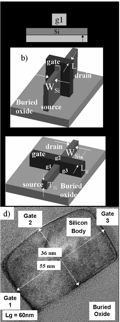
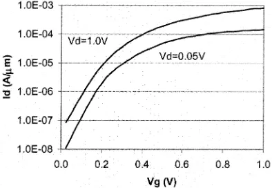
Fig. 1(a)–(c) shows schematics of the different types of FD transistor. Fig. 1(d) shows a TEM cross-section through the silicon body of a typical tri-gate transistor. The devices were fabricated as follows: the fin bodies were first fabricated by treating the body in a similar manner to polysilicon, using aggressive gate lithography techniques to get fin widths equal to gate lengths. The fins were then doped to obtain acceptable using conventional boron (for nMOS) or arsenic (for pMOS) implants. No halo implants were used for setting , nor were there any angled implants used anywhere in the process. This is in contrast to double-gate [7], and it is possible since the tri-gate very much resembles the bulk transistor from the processing point-of-view. The gate stack included polysilicon gates, and a conventional physical oxide thickness of 15 Å. Raised source/drains were used to reduce parasitic resistances [2]. Fig. 2 shows the – characteristics of an NMOS transistor whose TEM is shown in Fig. 1(d), while Fig. 3 shows the – characteristics of the same device. The transistor has physical
264 IEEE ELECTRON DEVICE LETTERS, VOL. 24, NO. 4, APRIL 2003
Fig. 1. Illustration of (a) single-gate, (b) double-gate, and (c) tri-gate transistor structures. (d) TEM cross section of the silicon body of the tri-gate NMOS device of Fig. 2.
nm, a height nm, and a width nm. This transistor exhibits excellent short channel effects with drain induced barrier lowering mV V (defined
as V V
where is taken at A m) and subthreshold slope mV dec.. The complete absence of any kink effect indicates that the device is fully depleted. The transistor also has a drive current (at V) equal to 1.14 mA m, and an off-current (at V) of 70 nA m.
Fig. 2. I –V characteristics of 60 nm gate length NMOS and PMOS transistors. The currentI is normalized to the width (Z) in all cases, where
Z = 2 3 T + W .
Fig. 3. I –V characteristics of the 60 nm N- and P-MOS devices of Fig. 2. The gate voltage was ramped to 1.3 V in increments of 0.1 V.
The width ( ) in all cases is taken to be , representing the top and the two sides of the tri-gate device. This drive current value is the highest reported for non-planar n-channel silicon devices with scaled threshold voltage (other devices have higher – e.g., [7] but the is many orders of magnitude higher). Fig. 2 also shows the – character-istics of the nm tri-gate PMOS device, which has A m and nA m at V, as well as mV V and mV dec.. These drive current values are also the highest reported for non-planar scaled p-channel silicon devices.
From Fig. 1(d), it can be seen that the silicon height ( 36 nm) for this tri-gate device is twice as large as that re-quired for full depletion in single-gate SOI devices at this gate length dimension [2]. The width of the silicon body ( 55 nm) is also approximately 50% greater than that required for full pletion in double-gate SOI transistors [4]. Thus, the tri-gate de-vices offer relaxed constraints in body dimensions over other FD transistor options (note that gate-all-around (GAA) [8] or wrap-around (WW) [9] gate devices are not considered here, due to the as-yet unresolved manufacturing difficulty of aligning the bottom gate without high overlap capacitance issues.)
DOYLEet al.: HIGH PERFORMANCE FD TRI-GATE CMOS TRANSISTORS 265
Fig. 4. I –V characteristics of a simulated NMOS tri-gate transistor, with
L = W = T = 30nm, showing subthreshold gradients of 73 mV/decade, and DIBL of 62 mV/V.
to the 1.14 and 0.52 mA m current values obtained for the tri-gates (Fig. 2), with a lower supply voltage (1.3 V), and a lower ( 70 nA m).
In order to study the scalability of these devices to smaller gate lengths, 3-D simulations were performed on tri-gate de-vices, using DESSIS [11]. This simulation extends the work of Leobandunget al.[9], taking it down to
nm. Similarly to Leobandunget al., the proximity of the
three gates in the tri-gate device was found to play an impor-tant role in controlling current conduction in the body of the de-vice, in contrast to the case of the planar dede-vice, where only the top surface is inverted. Fig. 4 shows the simulated - char-acteristics of the 30 nm device. It can be seen that the device shows near-ideal FD device performance with good DIBL and a steep subthreshold gradient. The simulations also show that the edge device turns on slightly before the bulk of the transistor. Since the edge is a significant proportion of the device width, the “hump” in the log - characteristics sometimes seen in narrow bulk devices is not seen in these tri-gate transistors.
These results suggest not only that the tri-gate concept is scal-able to future CMOS technology generations, but, given that the subthreshold gradient of bulk devices continues to degrade with shrinking gate length, the tri-gate transistor is a good candidate to replace bulk transistors in the near future.
III. SUMMARY
FD tri-gate CMOS transistors with gate lengths of 60 nm have been fabricated and compared to well-optimized bulk CMOS transistors at these dimensions. The tri-gate NMOS de-vice has a subthreshold slope mV decade, mV V, mA m and
nA m at V. The PMOS device shows mV decade, mV V, A m and nA m at V. To our knowledge, this is the highest performing non-planar CMOS devices with correctly targeted threshold voltages, and they compare well with optimized production-like bulk CMOS transistors with similar dimensions and processing.
The tri-gate devices show full depletion for much more relaxed silicon body dimensions than those required for single-gate or double-gate FD transistors, with full deple-tion achieved for a silicon body thickness ( nm) approximately double that required for single-gate, and a body width ( nm) approximately 1.5 times that required for double-gate SOI transistors at nm. Three–dimensional simulations of the tri-gate transistor with nm show that the tri-gate device main-tains full depletion at these dimensions, and exhibit excellent short channel performance, and suggest that this transistor design could supplant bulk CMOS transistors in the near future.
REFERENCES
[1] R. H. Yuan, A. Ourmazd, and K. Lee, “Scaling the Si MOSFET: From bulk to SOI to bulk,”IEEE Trans. Electron Devices, vol. 39, pp.
1704–1710, 1993.
[2] R. Chau, J. Kavalieros, B. Doyle, A. Murthy, N. Paulsen, D. Lionberger, D. Barlage, R. Arghavani, B. Roberds, and M. Doczy, “A 50 nm de-pleted-substrate CMOS transistor (DST),” inIEDM Tech. Dig., 2001,
pp. 621–624.
[3] H.-S. P. Wong, D. J. Frank, and P. M. Solomon, “Device design consid-erations for double-gate, ground-plane, and single-gated ultra-thin SOI MOSFET’s at the 25 nm channel length generation,” inIEDM Tech. Dig., 1998, pp. 407–410.
[4] N. Lindert, L. Chang, Y.-K. Cho, E. H. Anderson, W.-C. Lee, T.-J. King, J. Bokor, and C.-M. Hu, “Sub-60-nm quasiplanar FinFET’s fabricated using a simplified process,”IEEE Electron Device Lett., vol. 22, pp. 487–489, 2001.
[5] J.-T. Park, J.-P. Colinge, and C. H. Diaz, “Pi-Gate SOI MOSFET,”IEEE Electron Device Lett., vol. 22, pp. 405–406, 2001.
[6] R. Chau, B. Doyle, J. Kavalieros, D. Barlage, A. Murthy, M. Doczy, R. Arghavani, and S. Datta, “Advanced depleted-substrate transistors: Single-gate, double-gate and tri-gate,” inExt. Abst. 2002 Int. Conf. Solid State Devices & Materials, Nagoya, Japan, pp. 68–69.
[7] J. Kedzierskiet al., “High-Performance symmetric-gate and
CMOS-compatibleV tasymmetric-gate FinFET devices,” inIEDM Tech. Dig.,
2001, pp. 437–440.
[8] J.-P. Colinge, M. H. Gao, A. Romano-Rodriguez, H. Maes, and C. Claeys, “Silicon-on-Insulator gate-all-around device,” inIEDM Tech. Dig., 1990, pp. 595–598.
[9] E. Leobandung, J. Gu, L. Guo, and S.-Y. Chou, “Wire-channel and wrap-around-gate metal-oxide-semiconductor field-effect transistors with a significant reduction of short channel effects,”J. Vac. Sci. Technol. B,
vol. 15, pp. 2791–2794, 1997.
[10] S. Thompsonet al., “An enhanced 130 nm generation logic technology