Analog Interfacing to Embedded
Microprocessors
Analog Interfacing to Embedded
Microprocessors
Real World Design
Stuart Ball
Newnes is an imprint of Butterworth–Heinemann.
Copyright © 2001 by Butterworth–Heinemann A member of the Reed Elsevier group All rights reserved.
No part of this publication may be reproduced, stored in a retrieval system, or transmitted in any form or by any means, electronic, mechanical, photocopying, recording, or otherwise, without the prior written permission of the publisher.
Recognizing the importance of preserving what has been written, Butterworth–Heinemann prints its books on acid-free paper whenever possible.
Library of Congress Cataloging-in-Publication Data Ball, Stuart R., 1956–
Analog interfacing to embedded microprocessors : real world design / Stuart Ball. p. cm.
ISBN 0-7506-7339-7 (pbk. : alk. paper)
1. Embedded computer systems—Design and construction. 2. Microprocessors. I. Title.
TK7895.E42 .B33 2001
004.16—dc21 00-051961
British Library Cataloguing-in-Publication Data
A catalogue record for this book is available from the British Library.
The publisher offers special discounts on bulk orders of this book. For information, please contact:
Manager of Special Sales Butterworth-Heinemann 225 Wildwood Avenue Woburn, MA 01801-2041 Tel: 781-904-2500 Fax: 781-904-2620
For information on all Newnes publications available, contact our World Wide Web home page at: http://www.newnespress.com
10 9 8 7 6 5 4 3 2 1
Preface ix
Introduction xi
1 System Design 1
Dynamic Range 1 Calibration 2 Bandwidth 5
Processor Throughput 6 Avoiding Excess Speed 7 Other System Considerations 8 Sample Rate and Aliasing 11
2 Digital-to-Analog Converters 13
Analog-to-Digital Converters 15 Types of ADCs 17
Sample and Hold 26 Real Parts 29
Microprocessor Interfacing 30 Serial Interfaces 36
Multichannel ADCs 41
Internal Microcontroller ADCs 41
Codecs 42
Interrupt Rate 43
Dual-Function Pins on Microcontrollers 43 Design Checklist 45
3 Sensors 47
Measuring Period versus Frequency 95 Mixing 97
Voltage-to-Frequency Converters 99 Clock Resolution 102
5 Output Control Methods 103
Open-Loop Control 103
Negative Feedback and Control 103 Microprocessor-Based Systems 104 On-Off Control 105
Proportional Control 108 PID Control 110
Motor Control 123
Measuring and Analyzing Control Loops 130
6 Solenoids, Relays, and Other Analog Outputs 137
8 EMI 203
Ground Loops 203
ESD 208
9 High-Precision Applications 213
Input Offset Voltage 215 Input Resistance 216
Frequency Characteristics 217 Temperature Effects in Resistors 218 Voltage References 219
Temperature Effects in General 221 Noise and Grounding 222
Supply-Based References 227
10 Standard Interfaces 229
IEEE 1451.2 229
4-20 ma Current Loop 231
Appendix A: Opamp Basics 233
Four Opamp Configurations 233 General Opamp Design Equations 237 Reversing the Inputs 238
Comparators 239
Instrumentation Amplifiers 243
Appendix B: PWM 245
Why PWM? 245
Real Parts 250
Audio Applications 252
Appendix C: Some Useful URLs 255
Glossary 257
There often seems to be a division between the analog and digital worlds. Digital designers usually do not like to delve into analog, and analog design-ers tend to avoid the digital realm. The two groups often do not even use the same buzzwords.
Even though microprocessors have become increasingly faster and more capable, the real world remains analog in nature. The digital designers who attempt to control or measure the real world must somehow connect this analog environment to their digital machines. There are books about analog design and books about microprocessor design. This book attempts to get at the problems encountered in connecting the two together.
This book came about because of a comment made by someone about my first book (Embedded Microprocessor Systems: Real World Design): “it needs more analog interfacing information.” I felt that adding this material to that book would cause the book to lose focus. However, the more I thought about it, the more I thought that a book aimed at interfacing the real world to micro-processors could prove valuable. This book is the result. I hope it proves useful.
Modern electronic systems are increasingly digital: digital microprocessors, digital logic, digital interfaces. Digital logic is easier to design and understand, and it is much more flexible than the equivalent analog circuitry would be. As an example, imagine trying to implement any kind of sophisticated micro-processor with analog parts. Digital electronics lets the PC on your desk execute different programs at different times, perform complex calculations, and communicate via the World Wide Web.
While the electronic world is nearly all digital, the real world is not. The temperature in your office is not just hot or cold, but varies over a wide range. You can use a thermometer to determine what the temperature is, but how do you convert the temperature to a digital value for use in a microprocessor-controlled thermostat? The ignition control microprocessor in your car has to measure the engine speed to generate a spark at the right time. A micro-processor-controlled machining tool has to position the cutting bit in the right place to cut a piece of steel.
This book provides coverage of practical control applications and gives some opamp examples; however, its focus is neither control theory nor opamp theory. Primarily, its coverage includes measurement and control of analog quantities in embedded systems that are required to interface with the real world. Whether measuring a signal from a satellite or the temperature of a toaster, embedded systems must measure, analyze, and control analog values. That’s what this book is about—connecting analog input and output devices to microprocessors for embedded applications.
System Design
1
Most embedded microprocessor designs involve processing some kind of input to produce some kind of output, and one or both of these is usually analog. The digital portions of an analog system, such as the microprocessor-to-memory interface, are outside the scope of this book. However, there are some system considerations in any design that must interface to the real world, and these will be considered here.
Dynamic Range
Before a system can be designed, the dynamic range of the inputs and outputs must be known. The dynamic range defines the precision that must be applied to measuring the inputs or generating the outputs. This in turn drives other parts of the design, such as allowable noise and the precision that is required of the components.
A simple microprocessor-based system might read an analog input voltage and convert it to a digital value (how this happens will be examined in Chapter 2, “Digital-to-Analog Converters”). Dynamic range is usually expressed in db because it is usually a measurement of relative power or voltage. However, this does not cover all the things that a microprocessor-based system might want to measure. In simplest terms, the dynamic range can be thought of as the largest value that must be measured compared to (or divided by) the small-est. In most cases, the essential number that needs to be known is the number of bits of precision required to measure or control something.
same temperature range with .1°C accuracy? Now we need 100/.1, or 1000 discrete values, and that means a 10-bit ADC (which can produce 1024 dis-crete values).
Voltage Precision
The number of bits required to measure our example temperature range is dependent on the range of what we are measuring (temperature, voltage, light intensity, pressure, etc.) and not on a specific voltage range. In fact, our 0-to-100°C range might be converted to a 0-to-5 volt swing or a 0-to-1 volt swing. In either case, the dynamic range that we have to measure is the same. However, the 0-to-5V range uses 19.5 mV steps (5v/256) for 1°C accuracy and 4.8 mV steps (5v/1024) for .1°C accuracy. If we use a 0-to-1V swing, we have step sizes of 3.9 mV and 976mV. This affects the ADC choices, the selection of opamps, and other considerations. These will be examined in more detail in later chapters. The important point is that the dynamic range of the system determines how many bits of precision are needed to measure or control something; how that range is translated into analog and then into digital values further constrains the design.
Calibration
Dynamic range brings with it calibration issues. A certain dynamic range implies a certain number of bits of precision. But real parts that are used to measure real-world things have real tolerances. A 10K resistor can be between 9900 and 10,100 ohms if it has a 1% tolerance, or between 9990 and 10,010 ohms if it has .1% tolerance. In addition, the resistance varies with temperature. All the other parts in the system, including the sensors them-selves, have similar variations. While these will be addressed in more detail in Chapter 9, “High-Precision Applications,” the important thing from a system point of view is this: how will the required accuracy be achieved?
For example, say we’re still trying to measure that 0-to-100°C temperature range. Measurement with 1°C accuracy may be achievable without adjust-ments. However, you might find that the .1°C figure requires some kind of calibration because you can’t get a temperature sensor in your price range with that accuracy. You may have to include an adjustment in the design to compensate for this variation.
in the field? Will he be able to do the calibration? Will it really be cheaper, in production, to add a calibration step to the assembly procedure than to purchase a more accurate sensor?
In many cases where an adjustment is needed, the resulting calibration parameters can be calculated in software and stored. For example, you might bring the system (or just the sensor) to a known temperature and measure the output. You know that an ideal sensor should produce an output voltage X for temperature T, but the real sensor produces an output voltage Y for temperature T. By measuring the output at several temperatures, you can build up a table of information that relates the output of that specific sensorto temperature. This information can be stored in memory. When the micro-processor reads the sensor, it looks in the memory (or does a calculation) to determine the actual temperature.
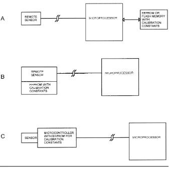
You would want to look at storing this calibration with the sensor if it is not physically located with the microprocessor. This way, the sensor can be changed without recalibrating. Figure 1.1 shows three means of handling this calibration.
In diagram A, a microprocessor connects to a remote sensor via a cable. The microprocessor stores the calibration information in its EEPROM or flash memory. The tradeoffs for this method are:
• Once the system is calibrated, the sensor has to stay with that micro-processor board. If either the sensor or the micromicro-processor is changed, the system has to be recalibrated.
• If the sensor or microprocessor is changed and recalibration is not performed, the results will be incorrect, but there is no way to know that the results are incorrect unless the microprocessor has a means to identify specific sensors.
• Data for all the sensors can be stored in one place, requiring less memory than other methods. In addition, if the calibration is performed by calcula-tion instead of by table lookup, all sensors that are the same can use the same software routines, each sensor just having different calibration constants.
Diagram B shows an alternate method of handling a remote sensor, where the EEPROM that contains the calibration data is located on the board with the sensor. This EEPROM could be a small IC that is accessed with an I2C or
microwire interface (more about those in Chapter 2, “Digital-to-Analog Conversion”). The tradeoffs here are:
• Since each sensor carries its own calibration information, sensors and microprocessor boards can be interchanged at will without affecting results. Spare sensors can be calibrated and stocked without having to be matched to a specific system.
Finally, diagram C takes this concept a step further, adding a micro-controller to the sensor board, with the micromicro-controller performing the cal-ibration and storing calcal-ibration data in an internal EEPROM or flash memory. The tradeoffs here are:
• More processors and more firmware to maintain. In some applications with rigorous software documentation requirements (medical, military) this may be a significant development cost.
• No calibration effort required by main microprocessor. For a given real-world condition, such as temperature, it will always get the same value, regardless of the sensor output variation.
• If a sensor becomes unavailable or otherwise has to be changed in pro-duction, the change can be made transparent to the main microprocessor Figure 1.1
code, with all the new characteristics of the new sensor handled in the remote microcontroller.
Another factor to consider in calibration is the human element. If a system requires calibration of a sensor in the field, does the field technician need arms twelve feet long to hold the calibration card in place and simultaneously reach the “ENTER” key on the keyboard? Should a switch be placed near the sensor so calibration can be accomplished without walking repeatedly around a table to hit a key or view the results on the display? Can the adjustment process be automated to minimize the number of manual steps required? The more manual adjustments that are needed, the more opportunities there are for mistakes.
Bandwidth
Several years ago, I worked on an imaging application. This system was to capture data using a CCD (Charge Coupled Device) image sensor. We were capturing 1024 pixels per scan. We had to capture items moving 150 inches per second at a resolution of 200 pixels per inch. Each pixel was converted with an 8-bit ADC, resulting in 1 byte per pixel. The data rate was therefore 150 ¥1024 ¥200, or 30,720,000 bytes per second.
We planned to use the VME bus as the basis for the system. Each scan from the CCD had to be read, normalized, filtered, and then converted to 1-bit-per-pixel monochrome. During the meetings that were held to establish the system architecture, one of the engineers insisted that we pass all the data through the VME bus. In those days, the VME bus had a maximum bandwidth specification of 40 megabytes per second, and very few systems could achieve the maximum theoretical bandwidth. The bandwidth we needed looked like this:
Read data from camera into system: 30.72 Mbytes/sec Pass data to normalizer: 30.72 Mbytes/sec
Pass data to filter: 30.72 Mbytes/sec
Pass data to monochrome converter: 30.72 Mbytes/sec Pass monochrome data to output: 3.84 Mbytes/sec
how much data you have to push around and what buses or data paths you are going to use. If you are using a standard interface such as Ethernet or Firewire, be sure it will support the total bandwidth required.
Processor Throughput
In many applications, the processor throughput is an important considera-tion. In the imaging example just mentioned, most of the functionality was performed in hardware because the available microprocessors could not keep up. As processor speeds increase, more functionality is pushed into the soft-ware. The key factors that you must consider to determine your throughput requirements are:
Interrupts
How often must the interrupts occur, and how much processing must be per-formed in each ISR (interrupt service routine)? What is the maximum allow-able latency for servicing an interrupt? Will interrupts need to be turned off for an extended length of time, and how will that affect the latency of other interrupts? You may find that you need two (or more) processors—one to handle high-speed interrupts with short latency requirements but low com-plexity processing needs, and another to handle low-rate interrupts with more complex processing requirements.
Interfaces
What must the system talk to? How will the data be passed around or get to the outside world? How much hardware support will there be for the inter-face and how much of the functionality will be performed in software? To take a simple example, an I2C interface that is implemented on a microcontroller by flipping bits in software will impact overall throughput more than an I2C interface that is implemented in hardware. This issue will likely be related to the interrupt considerations, because the interface will probably use inter-rupts. (If you don’t know what I2C is, it will be covered in Chapter 2, “Digital-to-Analog Converters.”)
Hardware Support
move the data in software but that has some kind of block-move instruction in the hardware will probably be faster than one that has to have a series of instructions to construct a loop. Similarly, if the CPU has an on-chip FPU (floating point coprocessor), then floating point operations will be much faster than if they have to be executed in software.
Processing Requirements
If you are working on an imaging application, having a processor move the data from one process (such as the camera interface logic) to another (such as filtering logic) takes some degree of processing. If the processor has to actu-ally implement the filtering algorithm in software, this takes a lot more pro-cessing horsepower. It is amazing how often systems are designed with little or no analysis of the amount of processing the CPU actually has to do.
Operating System Requirements
If you use an operating system (OS), how long will interrupts be turned off? Is this compatible with the interrupt latency requirements? What if the OS occasionally stops processing to spend a few seconds thrashing the hard disk? Will this cause data to be lost?
Language/Compiler
If you plan to use an object-oriented language such as C++, what happens when the CPU has to do garbage collection on the memory? Will data be lost? Does choosing this approach mean you have to go from a 100 MHz processor to a 500 MHz processor just to keep the garbage collection interval short?
Avoiding Excess Speed
Choosing a bus architecture and a processor that is fast enough to do the job is important, but it can also be important to avoid too much speed. It may not seem obvious that you wouldn’t always want the fastest bus and the fastest microprocessor, but there are applications where that is exactly the case. There are two basic reasons for this: cost and EMC (electromagnetic compatibility).
Cost
similar to the ISA bus used in personal computers and is capable of data trans-fers in the 5 Mbytes/sec range. Many CPU boards also have the PC/104 Plus bus, which has characteristics similar to the much faster (133 Mbytes/sec) PCI bus. Although it might seem that the faster bus is always preferred, it is often less expensive to design a peripheral board for the PC/104 bus than for the PC/104 Plus. PC/104, due to the slower clock rates, allows longer traces and simpler logic. If you have a relatively large analog I/O board plugged into a PC/104 CPU board, the relaxed timing constraints of PC/104 may make layout easier. Many low-volume products simply do not sell enough units to justify the higher development costs associated with PC/104 Plus. Of course, this assumes that the PC/104 bus will support the necessary data rates. Similar considerations apply to other buses, such as PCI and Compact PCI.
EMC
Almost every microprocessor-based design will have to undergo EMC (elec-tromagnetic compatibility) testing before it can be sold in the United States or Europe. EMC regulations limit the amount of energy the product can emit, to prevent interference with other equipment such as televisions and radios. Generally, the higher the clock rates are, the more emissions the equipment generates. Current EMC standards test radiated emissions in the frequency range between 30 MHz and 1 GHz. A processor running with a 6 MHz clock will not have any fundamental emissions in this range; the only frequencies in the test range will be those from the fifth and higher harmonics of the proces-sor clock. The higher harmonics typically have less energy. On the other hand, a 33 MHz processor will produce energy in the test band from its fundamen-tal frequency and higher. In addition, a faster processor clock rate means faster logic with faster edges and correspondingly higher energy in the harmonics. Although using a 6 MHz example in an era of 1000 MHz Pentiums may seem archaic, it does illustrate the point. EMC concerns are a valid reason to limit bus and processor speeds only to what is actually needed for the appli-cation. The caution here is not to limit the design too much. If the processor can just barely keep up with the application, there is no margin left to fix problems or add enhancements.
Other System Considerations
Peripheral Hardware
traced to the disk drive, where the drive would just stop accepting data for a while and the image buffers would overflow. It turned out that this particu-lar drive had a thermal compensation feature that required the on-drive CPU to “go away” for a few tens of milliseconds every so often. The application required continuous access to the drive. Be sure the peripheral hardware is compatible with your application and does not introduce problems.
Shared Interfaces
What is the impact of shared interfaces? For example, if you are continuously buffering data from two different image cameras on two disk drives, a single IDE interface may not be fast enough. You may need separate IDE interfaces for the two drives so they can operate independently, or you may need to go to a higher-performance interface. Similarly, will 10-baseT Ethernet handle all your data, or will you need 100-baseT? Look at allthe data on all the inter-faces and make sure the bandwidth you need is there.
Task Priorities
The IBM PC architecture has been used for all number of applications. It is a well-documented standard with an enormous number of compatible soft-ware packages available. But it has some drawbacks, including the non-real-time nature of the standard Windows operating system. You have probably experienced having your PC stop responding for a few seconds while it thrashes the hard disk for some unknown reason. If you are typing a docu-ment on a word processor, this is a minor annoyance—whatever you typed is captured (as long as it isn’t too many characters) and shows up on the screen whenever the operating system gets back to processing the keyboard.
What happens if you are getting a continuous stream of data from an audio or video device when this happens? If your system isn’t constructed to permit your data stream to have a high priority, some data may be lost. If you are using a PC-like architecture, be sure the hardware and operating system soft-ware will support the things you need to do.
Hardware Requirements
Do you need a floating-point processor to do calculations on the data you will be processing? If so, you won’t be able to use a simple 8-bit processor, you will need at least a 486-class machine. Does the data rate require a processor with a DMA controller in order to keep up? This limits your potential CPU selec-tions to just a few. In some cases, you can make system adaptaselec-tions that will lower hardware costs, as the following example will illustrate.
speeds and the processor has to schedule some event, such as activating a sole-noid to open a valve, some number of degrees after the interrupt occurs.
The 20° interrupts will occur 3.3 ms apart if the wheel spins at 1000 rpm, and 666mS apart if the wheel spins at 5000 RPM. If the processor uses a timer to measure the rotation speed (time between interrupts), and if the timer runs at 1 MHz, then the timer will increment 3300 counts between interrupts at 1000 RPM, and 666 counts at 5000 RPM.
Say that the CPU has to open our hypothetical solenoid when the wheel has rotated 5° past one of the interrupts, as shown in Figure 1.2. The formula for calculating the timer value (how much must be added to the current count for a 5° delay) looks like this:
So at 1000 RPM, the 5° delay is 825 timer counts, and at 5000 RPM, the delay is 166 counts. The problem with this approach in an embedded system is the need to divide by 20 in the formula. Division is a time-consuming task to perform in software, and this approach might require that you choose a processor with a hardware divide instruction.
If we change our measurement system so that the 20° divisions are divided into binary values, the math gets easier. Say that we decide to divide the 20° divisions into 32 equal parts, each part being .625 degrees. We’ll call these increments units just so we have a name for them. The 5° increment is now 5/.625 or 8 units. Now our formula looks like this:
Timer increment value = 5 degrees delay
20 degrees interrupt ¥Number of timer counts per interrupt Figure 1.2
This gives us the same result as before (825 at 1000 RPM, 166 at 5000 RPM), but division by 32 can be performed with a simple shift operation instead of a complex software algorithm. A change such as this may make the difference between a simple 8-bit microcontroller and a more complex and expensive microprocessor. All we did was change measuring degrees of rotation to mea-suring something that is easier to calculate.
Word Width
If you are connecting a processor to a 12-bit ADC, you will probably want a 16-bit processor instead of an 8-bit processor. While you can perform 16-bit operations on an 8-bit CPU, it usually requires multiple instructions and has other limitations. Unless the processor is simply passing the data on to some other part of the system, you will want to match the CPU to the devices with which it must interface. Similarly, if you will be performing calculations to 32-bit accuracy, you will want to consider a CPU with at least 16- and probably 32-bit word width to make computation easier and faster.
Interfaces
Be sure that interface conditions that are unusual but normal don’t cause damage to any part of the system. For instance, a microprocessor board may connect to a motor control board with a cable. What happens if the service engineer leaves the cable unplugged and turns the system on? Will the motors remain stationary, or will they run out of control? Make sure that issues like this are addressed.
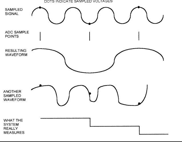
Sample Rate and Aliasing
Figure 1.3 shows a sinusoidal input signal and an ADC that is sampling slower than the signal is changing. If the system measuring this system assumed it was measuring a sinusoid of some frequency, it would conclude that it was measuring a sinusoid exactly half the frequency of the real input. This is called aliasing. Aliasing can occur any time that the input frequency is a multiple of the sample frequency.
Also shown in Figure 1.3 is another input waveform that is not a sinusoid. In this case, the system doesn’t assume it is sampling a sine, so it just stores
Timer increment value = 8 units
the samples as they are read. As you can see, the resulting pattern of data values does not match the input at all.
Any system must be designed so that it can keep up with whatever it is mea-suring. This includes the speed at which the ADC can collect samples and the speed at which the microprocessor can process them. If the input frequency will be greater than the measurement capability of the system, there are three ways to handle it:
1. Speed up the system to match the input.
2. Filter out high-frequency components with external hardware ahead of the ADC measuring the signal.
3. Filter out or ignore high-frequency components in software. This sounds silly—how do you filter something faster than you can measure? But if the valid input range is known, such as the number of cars entering a parking lot over any given time, then bogus inputs may be detectable. In this example, any input frequency greater than a couple per second can be assumed to be the result of noise or a faulty sensor—real cars don’t enter parking lots that fast.
Good system design depends on choosing the right tradeoffs between processor speed, system cost, and ease of manufacture.
Digital-to-Analog Converters
2
Although this chapter is primarily about analog-to-digital converters (ADCs), an understanding of digital-to-analog converters (DACs) is important to understanding how ADCs work.
Figure 2.1 shows a simple resistor ladder with three switches. The resistors are arranged in an R/2R configuration. The actual values of the resistors are unimportant; R could be 10K or 100K or almost any other value.
Each switch, S0–S2, can switch one end of one 2R resistor between ground and the reference input voltage, VR. The figure shows what happens when switch S2 is ON (connected to VR) and S1 and S2 are OFF (connected to ground). By calculating the resulting series/parallel resistor network, the final output voltage (VO) turns out to be .5 ¥VR. If we similarly calculate VO for all the other switch combinations, we get this:
S2 S1 S0 VO
OFF OFF OFF 0
OFF OFF ON .125 ¥VR (1/8 ¥VR)
OFF ON OFF .25 ¥VR (2/8 ¥VR)
OFF ON ON .375 ¥VR (3/8 ¥VR)
ON OFF OFF .5 ¥VR (4/8 ¥VR)
ON OFF ON .625 ¥VR (5/8 ¥VR)
ON ON OFF .75 ¥VR (6/8 ¥VR)
ON ON ON .875 ¥VR (7/8 ¥VR)
EQUIVALENT LOGIC
S0–S2 ON/OFF STATE STATE
NUMERIC S2 S1 S0 S2 S1 S0 EQUIVALENT
OFF OFF OFF 0 0 0 0
The output voltage is a representation of the switch value. Each additional table entry adds VR/8 to the total voltage. Or, put another way, the output voltage is equal to the binary, numeric value of S0–S2, times VR/8. This 3-switch DAC has 8 possible states and each voltage step is VR/8.
We could add another R/2R pair and another switch to the circuit, making a 4-switch circuit with 16 steps of VR/16 volts each. An 8-switch circuit would have 256 steps of VR/256 volts each. Finally, we can replace the mechan-ical switches in the schematic with electronic switches to make a true DAC.
Analog-to-Digital Converters
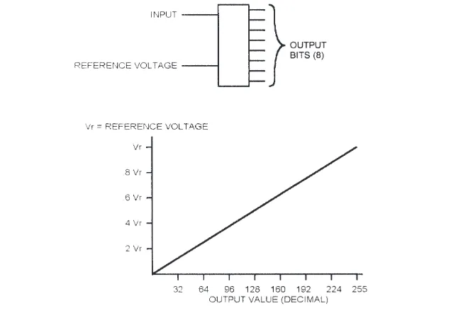
The usual method of bringing analog inputs into a microprocessor is to use an analog-to-digital converter (ADC). An ADC accepts an analog input, a voltage or a current, and converts it to a digital word that can be read by a microprocessor. Figure 2.2 shows a simple ADC. This hypothetical part has two inputs: a reference and the signal to be measured. It has one output, an 8-bit digital word that represents, in digital form, the input value. For the moment, ignore the problem of getting this digital word into the microprocessor.
Reference Voltage
This is the step size of the converter. It also defines the converter’s resolution.
Output Word
Our 8-bit converter represents the analog input as a digital word. The most significant bit of this word indicates whether the input voltage is greater than half the reference (2.5v, with a 5v reference). Each succeeding bit represents half of the previous bit, like this:
Bit: Bit 7 Bit 6 Bit 5 Bit 4 Bit 3 Bit 2 Bit 1 Bit 0
Volts: 2.5 1.25 .625 .3125 .156 .078 .039 .0195
So a digital word of 0010 1100 represents this: Reference Voltage 5V
256 V, or 19.5mv for a 5V reference
256 = =.0195
Bit: Bit 7 Bit 6 Bit 5 Bit 4 Bit 3 Bit 2 Bit 1 Bit 0
Volts: 2.5 1.25 .625 .3125 .156 .078 .039 .0195 Output
Value 0 0 1 0 1 1 0 0
Adding the voltages corresponding to each bit, we get:
.625 +.156 +.078 =.859 volts
Resolution
The resolution of an ADC is determined by the reference input and by the word width. The resolution defines the smallest voltage change that can be measured by the ADC. As mentioned earlier, the resolution is the same as the smallest step size, and can be calculated by dividing the reference voltage by the number of possible conversion values.
For the example we’ve been using so far, an 8-bit ADC with a 5v reference, the resolution is .0195 v (19.5 mv). This means that any input voltage below 19.5 mv will result in an output of 0. Input voltages between 19.5 and 39 mv will result in an output of 1. Between 39 mv and 58.6 mv, the output will be 3. Resolution can be improved by reducing the reference input. Changing from 5v to 2.5v gives a resolution of 2.5/256, or 9.7 mv. However, the maximum voltage that can be measured is now 2.5v instead of 5v.
The only way to increase resolution without changing the reference is to use an ADC with more bits. A 10-bit ADC using a 5v reference has 210, or 1024 possible output codes. So the resolution is 5v/1024, or 4.88 mv.
Types of ADCs
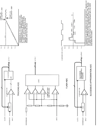
ADCs come in various speeds, use different interfaces, and provide differing degrees of accuracy. Three types of ADCs are illustrated in Figure 2.3.
Tracking ADC
The DAC input is connected to the counter output. Say the reference voltage is 5v. This would mean that the converter can convert voltages between 0v and 5v. If the most significant bit of the DAC input is “1,” the output voltage is 2.5v. If the next bit is “1,” 1.25v is added, making the result 3.75v. Each suc-cessive bit adds half the voltage of the previous bit, so the DAC input bits correspond to the following voltages:
Bit: Bit 7 Bit 6 Bit 5 Bit 4 Bit 3 Bit 2 Bit 1 Bit 0
Volts: 2.5 1.25 .625 .3125 .156 .078 .039 .0195
Figure 2.3 shows how the tracking ADC resolves an input voltage of .37v. The counter starts at zero, so the comparator output will be high. The counter counts up, once for every clock pulse, stepping the DAC output voltage up. When the counter passes the binary value that represents the input voltage, the comparator output will switch and the counter will count down. The counter will eventually oscillate around the value that represents the input voltage.
The primary drawback to the tracking ADC is speed—a conversion can take up to 256 clocks for an 8-bit output, 1024 clocks for a 10-bit value, and so on. In addition, the conversion speed varies with the input voltage. If the voltage in this example were .18v, the conversion would take only half as many clocks as the .37v example.
The maximum clock speed of a tracking ADC depends on the propagation delay of the DAC and the comparator. After every clock, the counter output has to propagate through the DAC and appear at the output. The compara-tor then takes some amount of time to respond to the change in DAC voltage, producing a new up/down control input to the counter.
Tracking ADCs are not commonly available; in looking at the parts avail-able from Analog Devices, Maxim, and Burr-Brown (all three are manufac-turers of ADC components), not one tracking ADC is shown. This only makes sense: a successive approximation ADC with the same number of bits is faster. However, there is one case where a tracking ADC can be useful. If the input signal changes slowly with respect to the sampling clock, a tracking ADC may produce an output in fewer clocks than a successive approximation ADC. I saw a design once that implemented a tracking ADC in discrete hardware in exactly this situation.
Flash ADC
256 comparators. One input of all the comparators is connected to the input to be measured.
The other input of each comparator is connected to one point in a string of resistors. As you move up the resistor string, each comparator trips at a higher voltage. All of the comparator outputs connect to a block of logic that determines the output based on which comparators are low and which are high.
The conversion speed of the flash ADC is the sum of the comparator delays and the logic delay (the logic delay is usually negligible). Flash ADCs are very fast, but take enormous amounts of IC real estate to implement. Because of the number of comparators required, they tend to be power hogs, drawing significant current. A 10-bit flash ADC IC may use half an amp.
Successive Approximation Converter
The successive approximation converter is similar to the tracking ADC in that a DAC/counter drives one side of a comparator while the input drives the other. The difference is that the successive approximation register performs a binary search instead of just counting up or down by one.
As shown in Figure 2.3, say we start with an input of 3v, using a 5v refer-ence. The successive approximation register would perform the conversion like this:
Set MSB of SAR, DAC voltage =2.5v.
Comparator output high, so leave MSB set
Result =1000 0000
Set bit 6 of SAR, DAC voltage =3.75v (2.5 +1.25)
Comparator output low, reset bit 6
Result =1000 0000
Set bit 5 of SAR, DAC voltage =3.125v (2.5 +.625)
Comparator output low, reset bit 5
Result =1000 0000
Set bit 4 of SAR, DAC voltage =2.8125v (2.5 +.3125)
Comparator output high, leave bit 4 set
Result =1001 0000
Set bit 3 of SAR, DAC voltage =2.968v (2.8125 +.15625)
Comparator output high, leave bit 3 set
Set bit 2 of SAR, DAC voltage =3.04v (2.968 +.078125)
Comparator output low, reset bit 2
Result =1001 1000
Set bit 1 of SAR, DAC voltage =3.007v (2.8125 +.039)
Comparator output low, reset bit 1
Result =1001 1000
Set bit 0 of SAR, DAC voltage =2.988v (2.8125 +.0195)
Comparator output high, leave bit 0 set
Final result =1001 1001
Using the 0-to-5v, 8-bit DAC, this corresponds to:
2.5 +.3125 +.15625 +.0195 or 2.98828 volts
This is not exactly 3v, but it is as close as we can get with an 8-bit converter and a 5v reference.
An 8-bit successive approximation ADC can do a conversion in 8 clocks, regardless of the input voltage. More logic is required than for the tracking ADC, but the conversion speed is consistent and usually faster.
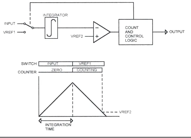
Dual-Slope (Integrating) ADC
A dual-slope converter (Figure 2.4) uses an integrator followed by a com-parator, followed by counting logic. The integrator input is first switched to the input signal, and the integrator output charges toward the input voltage. After a specified number of clock cycles, the integrator input is switched to a reference voltage (VREF1 in Figure 2.4) and the integrator charges down toward this value.
When the switch occurs to VREF1, a counter is started, and it counts using the same clock that determined the original integration time. When the inte-grator output falls past a second reference voltage (VREF2 in Figure 2.4), the comparator output goes high, the counter stops, and the count represents the analog input voltage.
Higher input voltages will allow the integrator to charge to a higher voltage during the input time, taking longer to charge down to VREF2, and resulting in a higher count at the output. Lower input voltages result in a lower inte-grator output and a smaller count.
since the same clock is used for charging and incrementing the counter. Note that clock jitter or drift within a single conversion will affect accuracy.
The dual-slope converter takes a relatively long time to perform a conver-sion, but the inherent filtering action of the integrator eliminates noise.
Sigma-Delta
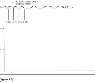
Before describing the sigma-delta converter, we need to look at how oversam-pling works, since it is key to understanding the sigma-delta architecture. Figure 2.5 shows a noisy 3v signal, with .2v peak-to-peak of noise. As shown in the figure, we can sample this signal at regular intervals. Four samples are shown in the figure; by averaging these we can filter out the noise:
Obviously this example is a little contrived, but it illustrates the point. If our system can sample the signal four times faster than data is actually needed, we can average four samples. If we can sample ten times faster, we can average ten samples for an even better result. The more samples we can average, the closer we get to the actual input value. The catch, of course, is that we have to run the ADC faster than we actually need the data, and have software to do the averaging.
3 05. v+3 1. V+2 9. V+2 95. V 4 3V
( ) =
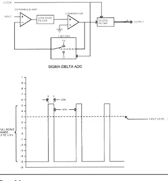
Figure 2.6 shows how a sigma-delta converter works. The input signal passes through one side of a differential amp, through a low-pass filter (integrator), and on to a comparator. The output of the comparator drives a digital filter and a 1-bit DAC. The DAC output can switch between +V and -V. In the example shown in Figure 2.6, +V is .5v, and -V is -.5V.
The output of the DAC drives the other side of the differential amp, so the output of the differential amp is the difference between the input voltage and the DAC output. In the example shown, the input is .3v, so the output of the differential amp is either .8v (when the DAC output is -.5v) or -.2v (when the DAC output is .5v).
The output of the low-pass filter drives one side of the comparator, and the other side of the comparator is grounded. So any time the filter output is above ground, the comparator output will be high, and any time the filter output is below ground, the comparator output will be low. The thing to remember is that the circuit tries to keep the filter output at 0v.
As shown in Figure 2.6, the duty cycle of the DAC output represents the input level; with an input of .3v (80% of the -.5 to .5v range), the DAC output has a duty cycle of 80%. The digital filter converts this signal to a binary digital value.
The input range of the sigma-delta converter is the plus-and-minus DAC voltage. The example in Figure 2.6 uses .5 and -.5v for the DAC, so the input range is -.5v to .5v, or 1v total. For ±1v DAC outputs, the range would be ±1v, or 2v total.
The primary advantage of the sigma-delta converter is high resolution. Since the duty cycle feedback can be adjusted with a resolution of one clock, the resolution is limited only by the clock rate. Faster clock = higher resolution.
All of the other types of ADCs use some type of resistor ladder or string. In the flash ADC the resistor string provides a reference for each compara-tor. On the tracking and successive approximation ADCs, the ladder is part Figure 2.6
of the DAC in the feedback path. The problem with the resistor ladder is that the accuracy of the resistors directly affects the accuracy of the conversion result. Although modern ADCs use very precise, laser-trimmed resistor networks (or sometimes capacitor networks), there are still some inaccuracies in the resistor ladders. The sigma-delta converter does not have a resistor ladder; the DAC in the feedback path is a single-bit DAC, with the output swinging between the two reference endpoints. This provides a more accu-rate result.
The primary disadvantage of the sigma-delta converter is speed. Because the converter works by oversampling the input, the conversion takes many clocks. For a given clock rate, the sigma-delta converter is slower than other converter types. Or, to put it another way, for a given conversion rate, the sigma-delta converter requires a faster clock.
Another disadvantage of the sigma-delta converter is the complexity of the digital filter that converts the duty cycle information to a digital output word. The sigma-delta converter has become more commonly available with the ability to add a digital filter or DSP to the IC die.
Half-Flash
Figure 2.7 shows a block diagram of a half-flash converter. This example implements an 8-bit ADC with 32 comparators, instead of 256. The half-flash converter has a 4-bit (16 comparators) flash converter to generate the MSB of the result. The output of this flash converter then drives a 4-bit DAC to generate the voltage represented by the 4-bit result. The output of the DAC is subtracted from the input signal, leaving a remainder that is converted by another 4-bit flash to produce the LS 4 bits of the result.
Figure 2.7
If the converter shown in Figure 2.7 were a 0–5v converter, converting a 3.1v input, then the conversion would look like this:
Upper flash converter output =9
Subtracter output =3.1v -2.8125v =.2875v
Half-flash converters can also use three stages instead of two; a 12-bit converter might have three stages of 4 bits each. The result of the MS 4 bits would be subtracted from the input voltage and applied to the middle 4-bit state. The result of the middle stage would be subtracted from its input and applied to the least significant 4-bit stage. A half-flash converter is slower than an equivalent flash converter, but uses fewer comparators, so it draws less current.
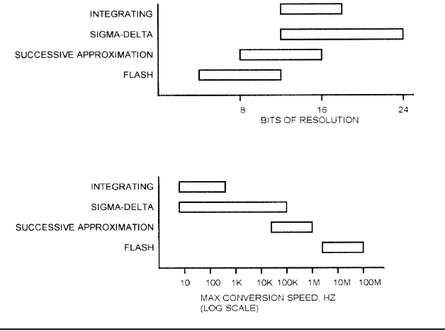
ADC Comparison
Figure 2.8 shows the range of resolutions available for integrating, sigma-delta, successive approximation, and flash converters. The maximum conversion speed for each type is shown as well. As you can see, the speed of available sigma-delta ADCs reaches into the range of the SAR ADCs, but is not as fast as even the slowest flash ADCs. What these charts do not show is tradeoffs between speed and accuracy. For instance, while you can get SAR ADCs that range from 8 to 16 bits, you won’t find the 16-bit version to be the fastest in a given family of parts. The fastest flash ADC won’t be the 12-bit part, it will be a 6- or 8-bit part.
These charts are a snapshot of the current state of the technology. As CMOS processes have improved, SAR conversion times have moved from tens of microseconds to microseconds. Not all technology improvements affect all types of converters; CMOS process improvements speed up all families of con-verters, but the ability to put increasingly sophisticated DSP functionality on the ADC chip doesn’t improve SAR converters. It does improve sigma-delta types.
Sample and Hold
ADC operation is straightforward when a DC signal is being converted. What happens when the signal is changing? Figure 2.9 shows a
Figure 2.8 ADC comparison.
Figure 2.9
ADC inaccuracy caused by a changing input.
ending up with a final result of 12710(7F16). The actual voltage at the end of the conversion is 2.8v, corresponding to a code of 14310(8F16).
The final code out of the ADC (127d) corresponds to a voltage of 2.48V. This is neither the starting voltage (2.3v) nor the ending voltage (2.8v). This example used a relatively fast input to show the effect; a slowly changing input has the same effect, but the error will be smaller.
One way to reduce these errors is to place a low-pass filter ahead of the ADC. The filter parameters are selected to insure that the ADC input does not change appreciably within a conversion cycle.
Another way to handle changing inputs is to add a sample-and-hold(S/H) circuit ahead of the ADC. Figure 2.10 shows how a sample-and-hold circuit works. The S/H circuit has an analog (solid state) switch with a control input. When the switch is closed, the input signal is connected to the hold capaci-tor and the output of the buffer follows the input. When the switch is open, the input is disconnected from the capacitor.
Figure 2.10 shows the waveform for S/H operation. A slowly rising signal is connected to the S/H input. While the control signal is low (sample), the output follows the input. When the control signal goes high (hold), discon-necting the hold capacitor from the input, the output stays at the value the input had when the S/H switched to hold mode. When the switch closes again, the capacitor charges quickly and the output again follows the input. Typically, the S/H will be switched to hold mode just before the ADC
version starts, and switched back to sample mode after the conversion is complete.
In a perfect world, the hold capacitor would have no leakage and the buffer amplifier would have infinite input impedance, so the output would remain stable forever. In the real world, the hold capacitor will leak and the buffer amplifier input impedance is finite, so the output level will slowly drift down toward ground as the capacitor discharges.
The ability of an S/H to maintain the output in hold mode is dependent on the quality of the hold capacitor, the characteristics of the buffer ampli-fier (primarily input impedance), and the quality of the sample/hold switch (real electronic switches have some leakage when open). The amount of drift exhibited by the output when in hold mode is called the droop rate, and is spec-ified in millivolts per second, microvolts per microsecond, or millivolts per microsecond.
A real S/H also has finite input impedance, because the electronic switch isn’t perfect. This means that, in sample mode, the hold capacitor is charged through some resistance. This limits the speed with which the S/H can acquire an input. The time that the S/H must remain in sample mode in order to acquire a full-scale input is called the acquisition time, and is specified in nanoseconds or microseconds.
Since there is some impedance in series with the hold capacitor when sam-pling, the effect is the same as a low-pass R-C filter. This limits the maximum frequency that the S/H can acquire. This is called the full power bandwidth, specified in kHz or MHz.
As mentioned, the electronic switch is imperfect and some of the input signal appears at the output, even in hold mode. This is called feedthrough, and is typically specified in db.
The output offset is the voltage difference between the input and the output. S/H datasheets typically show a hold mode offset and sample mode offset, in millivolts.
Real Parts
Real ADC ICs come with a few real-world limitations and some added features.
Input Levels
can be configured so that this 10v range is either 0 to 10v or -5v to +5v, using one pin. Of course, the device needs a negative voltage supply. Other common input voltage ranges are ±2.5v and ±3v.
With the trend toward lower-powered devices and small consumer equip-ment, the trend in ADC devices is to lower voltage, single-supply operation. Traditional single-supply ADCs have operated from +5V and had an input range between 0v and 5v. Newer parts often operate at 3.3 or 2.7v, and have an input range somewhere between 0v and the supply.
Internal Reference
Many ADCs provide an internal reference voltage. The Analog Devices AD872 is a typical device with an internal 2.5v reference. The internal reference voltage is brought out to a pin and the reference input to the device is also connected to a pin. To use the internal reference, the two pins are connected together. To use your own external reference, connect it to the reference input instead of the internal reference.
Reference Bypassing
Although the reference input is usually high impedance, with low DC current requirements, many ADCs will draw current from the reference briefly while a conversion is in process. This is especially true of successive approximation ADCs, which draw a momentary spike of current each time the analog switch network is changed. Consequently, most ADCs require that the reference input be bypassed with a capacitor of .1mf or so.
Internal S/H
Many ADCs, such as the Maxim MAX191, include an internal S/H. An ADC with an internal S/H may have a separate pin that controls whether the S/H is in sample or hold mode, or the switch to hold mode may occur automati-cally when a conversion is started.
Microprocessor Interfacing
Output Coding
2’s complement value. A few ADCs output values in BCD. Obviously this requires more bits for a given range; a 12-bit binary output can represent values from 0 to 4095, but a 12-bit BCD output can only represent values from 0 to 999.
Parallel Interfaces
ADCs come in a variety of interfaces, intended to operate with multiple processors. Some parts include more than one type of interface to make them compatible with as many processor families as possible.
The Maxim MAX151 is a typical 10-bit ADC with an 8-bit “universal” par-allel interface. As shown in Figure 2.11, the processor interface on the MAX151 has 8 data bits, a chip select (-CS), a read strobe (-RD), and a -BUSY output.
The MAX151 includes an internal S/H. On the falling edge of -RD and -CS, the S/H is placed into hold mode and a conversion is started. If -CS and -RD do not go low at the same time, the last falling edge starts a con-version. In most systems, -CS is connected to an address decode and will go low before -RD. As soon as the conversion starts, the ADC drives -BUSY low (active). -BUSY remains low until the conversion is complete.
In the first mode of operation, which Maxim calls Slow Memory Mode, the processor waits, holding -RD and -CS low, until the conversion is com-plete. In such a system, the -BUSY signal would typically be connected to the processor -RDY or -WAIT signal. This holds the processor in a wait state until the conversion is complete. The maximum conversion time for the MAX151 is 2.5ms.
The second mode of operation is called ROM mode. Here the processor performs a read cycle, which places the S/H in hold mode and starts a con-version. During this read, the processor reads the results of the previous conversion. The -BUSY signal is not used to extend the read cycle. Instead, -BUSY is connected to an interrupt, or is polled by the processor to indicate when the conversion is complete. When -BUSY goes high, the processor does another read to get the result and start another conversion.
Although the data sheets refer to two different modes of operation, the ADC works the same way in both cases:
• Falling edge of -RD and -CS starts a conversion
• Current result is available on bus after read access time has elapsed
• As long as -RD and -CS stay low, current result remains available on bus
The MAX151 is designed to interface to most microprocessors. Actually interfacing to a specific processor requires analysis of the MAX151 timing and how it relates to the microprocessor timing.
Data Access Time
The MAX151 specifies a maximum access time of 180 ns over the full tem-perature range (see Figure 2.12). This means that the result of a conversion Figure 2.11
will be available on the bus no more than 180 ns after the falling edge of -RD (assuming -CS is already low when -RD goes low). The processor will need the data to be stable some time before the rising edge of -RD. If there is a data bus buffer between the MAX151 and the processor, the propagation delay through the buffer must be included. This means that the processor bus Figure 2.12
cycle (the time that -RD is low) must be at least as long as the access time of the MAX151, plus the processor data setup time, plus any bus buffer delays.
-BUSY Output
The -BUSY output of the MAX151 goes low a maximum of 200 ns after the falling edge of -RD. This is too long for the signal to directly drive most micro-processors if you want to use the slow memory mode. Most micromicro-processors require that the RDY or -WAIT signal be driven low earlier in the bus cycle than this. Some require the wait request signal to be low one clock after -RD goes low.
The only solution to this problem is to artificially insert wait states to the bus cycle until the -BUSY signal goes low. Some microprocessors, such as the 80188 family, have internal wait state generators that can add wait states to a bus cycle. The 80188 wait-state generator can be programmed to add 0, 1, 2, or 3 wait states.
As shown in Figure 2.12, in Slow Memory mode the -BUSY signal goes high just before the new conversion result is available; according to the datasheet, this time is a maximum of 50 ns. For some processors, this means that the wait request must be held active for an additional clock cycle after -BUSY goes high to insure that the correct data is read at the end of the bus cycle.
Bus Relinquish
The MAX151 has a maximum bus relinquish time of 100 ns. This means that the MAX151 can drive the data bus up to 100 ns after the -RD signal goes high. If the processor tries to start another cycle immediately after reading the MAX151 result, this may result in bus contention. A typical example would be the 80186 processor, which multiplexes the data bus with the address bus; at the start of a bus cycle the data bus is not tristated, but the processor drives the address onto the data bus. If the MAX151 is still driving the bus, this can result in an incorrect bus address being latched.
Coupling
The MAX151 has an additional specification, not found on some ADCs, that involves coupling of the bus control signals into the ADC. Because modern ADCs are built as a monolithic IC, the part shares some internal components, such as the power supply pins and the substrate on which the IC die is con-structed. It is sometimes difficult to keep the noise generated by the micro-processor data bus and control signals from coupling into the ADC and affecting the result of a conversion.
To minimize the effect of coupling, the MAX151 has a specification that the -RD signal be no more than 300 ns wide when using ROM mode. This prevents the rising edge of -RD from affecting the conversion.
Delay between Conversions
When the MAX151 S/H is in sampling mode, the hold capacitor is connected to the input. This capacitance is about 150 pf. When a conversion starts, this capacitor is disconnected from the input. When a conversion ends, the capac-itor is again connected to the input, and it must charge up to the value of the input pin before another conversion can start. In addition, there is an inter-nal 150 ohm resistor in series with the input capacitor. Consequently, the MAX151 specifies a delay between conversions of at least 500 ns if the source impedance driving the input is less than 50W. If the source impedance is more than 1 KW, the delay must be at least 1.5ms. This delay is the time from the rising edge of -BUSY to the falling edge of -RD.
LSB Errors
In theory, of course, an infinite amount of time is required for the capacitor to charge up, because the charging curve is exponential and the capacitor never reaches the input voltage. In practice, the capacitor does stop charg-ing. More importantly, the capacitor only has to charge to within 1 bit (called 1 LSB) of the input voltage; for a 10v converter with a ±4v input range, this is 8v/1024, or 7.8 mv.
This is an important concept that we will take a closer look at later, in Chapter 9, “High-Precision Applications.” To simplify the concept, errors that fall within one bit of resolution have no effect on conversion accuracy. The other side of that coin is that the accumulation of errors (opamp offsets, gain errors, etc.) cannot exceed one bit of resolution or they willaffect the result.
Clocked Interfaces
proces-sor on a clock edge, rather than on the rising edge of a control signal such as -RD. These buses are often implemented on very fast processors and are usually capable of high-speed burst operation.
Shown in Figure 2.13 is a normal bus cycle without wait states. This bus cycle would be accessing a memory or peripheral that can operate at the full bus speed. The address and status information is provided on one clock, and the CPU reads the data on the next clock.
Following this cycle is an access to the MAX151. As can be seen, the MAX151 is much slower than the CPU, so the bus cycle must be extended with wait states (either internally or externally generated). This diagram is an example; the actual number of wait states that must be added depends on the processor clock rate. The bus relinquish time of the MAX151 will interfere with the next CPU cycle, so a buffer is necessary. Finally, since the CPU does not generate a -RD signal, one must be synthesized by the logic that decodes the address bus and generates timing signals to memory and peripherals.
The normal method of interfacing an ADC like this to a fast processor is to use the ROM mode. Slow Memory mode holds the CPU in a wait state for a long time—the 2.5ms conversion time of the MAX151 would be 82 clocks on a 33 MHz 80960. This is time that could be spent executing code.
Serial Interfaces
SPI/Microwire
SPI is a serial interface that uses a clock, chip select, data in, and data out bits. Data is read from a serial ADC a bit at a time (Figure 2.14). Each device on the SPI bus requires a separate chip select (-CS) signal.
Figure 2.13
The Maxim MAX1242 is a typical SPI ADC. The MAX1242 is a 10-bit suc-cessive approximation ADC with an internal S/H, in an 8-pin package. Figure 2.15 shows the MAX1242 interface timing. The falling edge of -CS starts a conversion, which takes a maximum of 7.5ms. When -CS goes low, the MAX1242 drives its data output pin low. After the conversion is complete, the MAX1242 drives the data output pin high. The processor can then read the data a bit at a time by toggling the clock line and monitoring the MAX1242 data output pin.
After the 10 bits are read, the MAX1242 provides two sub-bits, S1 and S0. If further clock transitions occur after the 13 clocks, the MAX1242 outputs zeros.
Figure 2.15 shows how a MAX1242 would be connected to a microcon-troller with an on-chip SPI/Microwire interface. The SCLK signal goes to the SPI SCLK signal on the microcontroller, and the MAX1242 DOUT signal con-nects to the SPI data input pin on the microcontroller. One of the micro-controller port bits generates the -CS signal to the MAX1242.
Note that the -CS signal starts the conversion and must remain low until the conversion is complete. This means that the SPI bus is unavailable for com-municating with other peripherals until the conversion is finished and the result has been read. If there are interrupt service routines that communicate with SPI devices in the system, they must be disabled during the conversion.
To avoid this problem, the MAX1242 could communicate with the controller over a dedicated SPI bus. This would use 3 more pins on the micro-controller. Since most microcontrollers that have on-chip SPI have only one, the second port would have to be implemented in software.
Finally, it is possible to generate an interrupt to the microcontroller when the ADC conversion is complete. An extra connection is shown in Figure 2.15, from the MAX1242 DOUT pin to an interrupt on the microcontroller. When -CS is low and the conversion is completed, DOUT will go high, interrupt-ing the microcontroller. To use this method, the firmware must ignore the interrupt except when a conversion is in process.
Another ADC with an SPI-compatible interface is the Analog Devices AD7823. Like the MAX1242, the AD7823 uses 3 pins: SCLK, DOUT, and -CONVST. The AD7823 is an 8-bit successive approximation ADC with inter-Figure 2.14
Figure 2.15
Maxim MAX1242 interface.
nal S/H. A conversion is started on the falling edge of -CONVST, and takes 5.5ms. The rising edge of -CONVST enables the serial interface.
Unlike the MAX1242, the AD7823 does not drive the data pin until the microcontroller reads the result, so the SPI bus can be used to communicate with other devices while the conversion is in process. However, there is no indication to the microprocessor when the conversion is complete—the processor must start the conversion, then wait until the conversion has had time to complete before reading the result. One way to handle this is with a regular timer interrupt: on each interrupt, the result of the previous conver-sion is read and a new converconver-sion is started.
I2C Bus
The I2C bus uses only two pins: SCL (SCLock) and SDA (SDAta). SCL is gen-erated by the processor to clock data into and out of the peripheral device. SDA is a bidirectional line that serially transmits all data into and out of the peripheral. The SDA signal is open-collector so several peripherals can share the same 2-wire bus.
peripher-als on the bus will interpret this as a START condition. SDA going high while SCL is high is a STOP or END condition.
Figure 2.16 illustrates a typical data transfer. The processor initiates the START condition, then sends the peripheral address, which is 7 bits long and tells the devices on the bus which one is to be selected. This is followed by a read/write bit (1 for read, 0 for write).
After the read/write bit, the processor programs the I/O pin connected to the SDA bit to be an input and clocks an acknowledge bit in. The selected peripheral will drive the SDA line low to indicate that it has received the address and read/write information.
After the acknowledge bit, the processor sends another address, which is the internal address within the peripheral that the processor wants to access. The length of this field varies with the peripheral. After this is another acknowledge, then the data is sent. For a write operation, the processor clocks out 8 data bits; for a read operation, the processor treats the SDA pin as an input and clocks in 8 bits. After the data comes another acknowledge.
Some peripherals permit multiple bytes to be read or written in one trans-fer. The processor repeats the data/acknowledge sequence until all the bytes are transferred. The peripheral will increment its internal address after each transfer.
One drawback to the I2C bus is speed—the clock rate is limited to about 100 KHz. A newer Fast-mode I2C bus that operates to 400 Kbits/sec is also avail-able, and a high-speed mode that goes to 3.4 Mbits/sec is also available. High-speed and fast-mode both support a 10-bit address field so up to 1024 locations can be addressed. High-speed and fast-mode devices are capable of operating in the older system, but older peripherals are not useable in a higher-speed system. The faster interfaces have some limitations, such as the need for active pullups and limits on bus capacitance. Of course, the faster modes of operation require hardware support and are not suitable for a software-controlled implementation.
A typical ADC using I2C is the Philips PCF8591. This part includes both an ADC and a DAC. Like many I2C devices, the 8591 has three pins: A0, A1, and A2. These can be connected to either “1” or “0” to select which address the device responds to. When the peripheral address is decoded, the PCF8591 will respond to address 1001xxx, where xxx matches the value of the A2, A1, and A0 pins. This allows up to eight PCF8591 devices to share a single I2C bus.
Proprietary Serial Interfaces
Some ADCs have a proprietary interface. The Maxim MAX1101 is a typical device. This is an 8-bit ADC that is optimized for interfacing to CCDs (charge-coupled devices). The MAX1101 uses four pins: MODE, LOAD, DATA, and SCLK. The MODE pin determines whether data is being written or read (1 =read, 0 =write). The DATA pin is a bidirectional signal, the SCLK signal clocks data into and out of the device, and the LOAD pin is used after a write to clock the write data into the internal registers.
The clocked serial interface of the MAX1101 is similar to SPI, but since there is no chip select signal, multiple devices cannot share the same data/clock bus. Each MAX1101 (or similar device), needs 4 signals from the processor for the interface.
Many proprietary serial interfaces are intended to be used with microcon-trollers that have on-chip hardware to implement synchronous serial I/O. The 8031 family, for example, has a serial interface that can be configured as either an asynchronous interface or as a synchronous interface. Many ADCs can connect directly to these types of microprocessors.
The problem with any serial interface on an ADC is that it limits conver-sion speed. In addition, the type of interface limits speed as well. Since every I2C exchanges involves at least 20 bits, an I2C device will never be as fast as an equivalent SPI or proprietary device. For this reason, there are many more ADCs available with SPI/Microwire than with I2C interfaces.
The required throughput of the serial interface drives the design. If you need a conversion speed of 100,000 8-bit samples per second and you plan to implement an SPI-type interface in software, then your processor will not be able to spend more than 1/(100,000 ¥8) or 1.25mS transferring each bit. This may be impractical if the processor has any other tasks to perform, so you may want to use an ADC with a parallel interface or choose a processor with hardware support for the SPI.