This content has been downloaded from IOPscience. Please scroll down to see the full text.
Download details:
IP Address: 101.203.171.4
This content was downloaded on 08/06/2017 at 06:28
Please note that terms and conditions apply.
Crystal Structure, Optical, and Electrical Properties of SnSe and SnS Semiconductor Thin
Films Prepared by Vacuum Evaporation Techniques for Solar Cell Applications
View the table of contents for this issue, or go to the journal homepage for more
1234567890
The 4th International Conference on Advanced Materials Science and Technology IOP Publishing IOP Conf. Series: Materials Science and Engineering 202 (2017) 012042 doi:10.1088/1757-899X/202/1/012042
Crystal Structure, Optical, and Electrical Properties of SnSe
and SnS Semiconductor Thin Films Prepared by Vacuum
Evaporation Techniques for Solar Cell Applications
Ariswan1, H Sutrisno2 and R Prasetyawati1 1
Department of Physics Education, Faculty of Mathematics and Natural Sciences, Yogyakarta State University, Kampus Karangmalang, Jl. Colombo 1, Yogyakarta, 55281, Indonesia
2
Department of Chemistry Education, Faculty of Mathematics and Natural Sciences, Yogyakarta State University, Kampus Karangmalang, Jl. Colombo 1, Yogyakarta, 55281, Indonesia
Email: [email protected]
Abstract. Thin films of SnSe and SnS semiconductors had been prepared by vacuum evaporation techniques. All prepared samples were characterized on their structure, optical, and electrical properties in order to know their application in technology. The crystal structure of SnSe and SnS was determined by X-Ray Diffraction (XRD) instrument. The morphology and chemical composition were obtained by Scanning Electron Microscopy (SEM) coupled with Energy Dispersive of X-Ray Analysis (EDAX). The optical property such as band gap was determined by DR-UV-Vis (Diffuse Reflectance-Ultra Violet-Visible) spectroscopy, while the electrical properties were determined by measuring the conductivity by four probes method.The characterization results indicated that both SnSe and SnS thin films were polycrystalline. SnSe crystallized in an orthorhombic crystal system with the lattice parameters of a = 11.47 Å, b = 4.152 Å and c = 4.439 Å, while SnS had an orthorhombic crystal system with lattice parameters of a = 4.317 Å, b = 11.647 Å and c = 3.981 Å. Band gaps (Eg) of SnSe and SnS were 1.63 eV and 1.35 eV, respectively. Chemical compositions of both thin films were non-stoichiometric. Molar ratio of Sn : S was close to ideal which was 1 : 0.96, while molar ratio of Sn : S was 1 : 0.84. The surface morphology described the arrangement of the grains on the surface of the thin film with sizes ranging from 0.2 to 0.5 microns. Color similarity on the surface of the SEM images proved a homogenous thin layer.
Keywords: Vacuum evaporation, solar cell, SnSe semiconductor, SnS semiconductor.
1.Introduction
2 1234567890
The 4th International Conference on Advanced Materials Science and Technology IOP Publishing IOP Conf. Series: Materials Science and Engineering 202 (2017) 012042 doi:10.1088/1757-899X/202/1/012042
obtained SnSe using Aqueous Solution Method [3], and had also been reported that SnSe thin film were prepared by photoelectrochemical techniques deposition [4]. Research on SnS thin film had also been successfully produced by spray pyrolysis method [5], electrodeposition technique [6] and of course with other techniques.
2.Experimental Procedure
2.1 Preparation of SnSe and SnS Semiconductors
At first, the vacuum system equipment consisting of a primary pump in the form of rotary van pump
capable of suppressing the pressure up to 10-3 Torr was prepared. The primary pump was connected to
the secondary pump in the form of diffusion pumps which were capable of decreasing the pressure of evaporator chamber at 10-6 Torr. Evaporator was equipped with boat-shaped crucible made of molybdenum (Mo) and connected to a power supply system that can generate electrical currents of up to 300 A. Crucible was mounted above the support where the substrates can be put and equipped with electrodes that can be connected to a power supply to set the substrate temperature.
SnSe powder was placed on the crucible, and then heated by slowly flowing current to crucible until the temperature reached above 1000 °C. The powder reached the point of vapor and deposited on the substrate at a temperature of 500 oC. After the deposition,the thin layers were left for 12 hours and then the evaporator was opened and a number of thin films were obtained. An equal treatment was
Bragg configuration using Cu Kα radiation (λ = 1.5406 Å). The XRD instrument ran at 40 kV and 15
mA. The intensities were determined in the 2θ interval ranging from 3° to 90°. The surface
morphology and chemical composition of SnSe and SnS thin films were investigated byScanning Electron Microscopy (SEM) coupled with Energy Dispersive Analysis of X-Ray (EDAX). To calculate the energy gap of the prepared samples, Diffuse Reflectance UV-Vis-UV 1700 Pharmaspec Spectroscopy at wavelengths ranged from 200 nm up to 900 nm was used. To specify the electrical properties such as conductivity and resistivity of the thin films, four-point probe technique was used.
3.Results and Discussion
SnSe and SnS thin films have been successfully obtained by vacuum evaporation techniques through the implementation of following variables variation. Variable control include vacuum pressure, the mass of material, and the temperature source (crucible) and the distance between the crucible and substrate, while the independent variables in this study were four variations of the temperature of the substrate, namely without heating, 250, 350, 500 and 550 oC [7]. In this article, only substrate temperature at 500 oC was reported to get the best values of the physical parameters after the characterization had been done. The characterization includes the structure and parameters of the crystal, the composition of the sample, optical properties and electrical properties of the thin film prepared using vacuum evaporation techniques.
3.1 XRD spectra of SnSe and SnS thin films
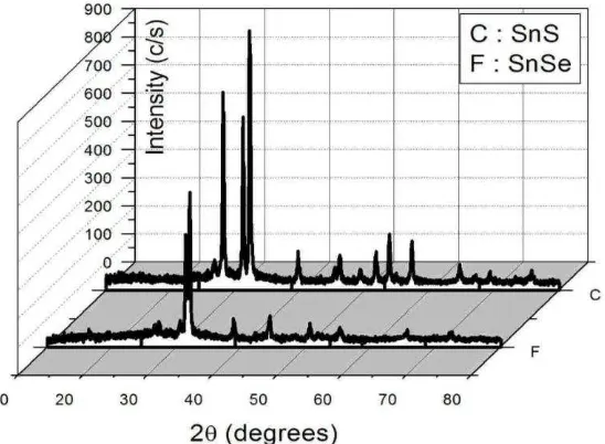
XRD (X-Ray Diffraction) can be used to determine the crystal lattice parameters and the structure of thin films. The data obtained from XRD analysis were in the form of a graph of intensity (I) and the spectrum of diffraction angle (2θ). Diffractogram displays spectral peaks that appeared in the samples. XRD analysis showed the distance among the crystal planes hkl (dhkl). Diffraction patterns obtained
1234567890
The 4th International Conference on Advanced Materials Science and Technology IOP Publishing IOP Conf. Series: Materials Science and Engineering 202 (2017) 012042 doi:10.1088/1757-899X/202/1/012042
The calculation of parameters can also be done once the crystal structure was known. Figure 1 shows the diffractogram of SnSe and SnS samples. The lattice parameters of orthorhombic crystal system can be calculated using the following equation [8].
2d sin θ = nλ
d , so the following relationship can be applied:
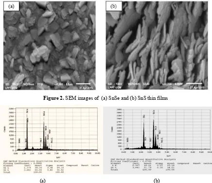
electron beams. The results of SEM characterization were images that depicted the surface of a crystal. The surface morphology characterization of SnSe and SnS samples with 40,000 times magnification is shown in Figure 2.
4 1234567890
The 4th International Conference on Advanced Materials Science and Technology IOP Publishing IOP Conf. Series: Materials Science and Engineering 202 (2017) 012042 doi:10.1088/1757-899X/202/1/012042
Figure 2. SEM images of (a) SnSe and (b) SnS thin films
(a) (b)
Figure 3. EDAX on chemical compositions of (a) SnSe and (b) SnS samples
Based on the morphological images resulted from the characterization by SEM as in Figure 2, it appears that there is homogeneity of Se and S crystals in the thin film. The SEM images showed that the structures of the sample are in bead and angled beam shapes and scattered on a regular basis. The granular form according to orthorhombic crystal structure which has an axis perpendicular to each other and had one parameter longer compared with the two other lattice parameters. The chemical composition of the thin films analyzed by EDAX can be seen in Figure 3.
1234567890
The 4th International Conference on Advanced Materials Science and Technology IOP Publishing IOP Conf. Series: Materials Science and Engineering 202 (2017) 012042 doi:10.1088/1757-899X/202/1/012042
3.3 Optical and electrical properties
The sample characterization for optical properties was carried out by UV-VIS spectroscopy with a wavelength ranged from 200 nm up to 900 nm. This equipment was not perfect because it could not reach up to the NIR with a wavelength of about 4000 nm. However, specifically for SnSe and SnS materials, it can be used to show the band gap width of both materials in the wavelength range of the spectrum. The absorption of wavelength can occur when radiation passes through the band gap of the material.
The phenomenon arose when inside the energy is passed so that the absorbance is very smalla band gap. When a photon of energy was equal to or greater than the band gap, the absorption will occur so
that the absorbance (A) would go up significantly. The absorbance spectrum as a function of photon
energy can be shown in Figure 4.
The calculation of the band gap of materials can be done using the formulation as follows. Absorption coefficient α is proportional to the absorbance A, so it can be stated that α = 2.303A/d, where d is the thickness of the thin films. Then the relationship between α and the photon energy hν
for direct band gap semiconductor material was given by the equation of
,h
2 B2
hvEg
, where B is a constant between 105 and 106 cm-1eV-1 [11]. The result of this calculation produced the width of SnSe and SnS band gaps of 1.63 eV and 1.35 eV respectively. The results are consistent with the results obtained by other researchers [12,13].The data, such as shown in Figure 4, can be processed to produce (α, hν)2 as a function of photon energy hν as shown in Figure 5. Based on the measurement of electrical properties, it can be seen that all SnSe and SnS samples hadthe same conductivity type,which is p-type, with average specific resistivity of 4.6 10-2 ohm-cm and 4.4 x 10⁻² ohm-cm, respectively. Both samples were prepared atthe same substrate temperature which was 500 oC. This result was in accordance with the range of resistance values of semiconductor materials.
6 1234567890
The 4th International Conference on Advanced Materials Science and Technology IOP Publishing IOP Conf. Series: Materials Science and Engineering 202 (2017) 012042 doi:10.1088/1757-899X/202/1/012042
Figure 5. (.h)2 as a function of photon energy h of SnS and SnSe thin layers
4.Conclusion
SnSe and SnS semiconductor thin films had been successfully prepared by vacuum evaporation techniques. The thin films were composed of atoms in orthorhombic crystal structure with the lattice parameters of a = 11.47 Å; b= 4.152 Å and c = 4.439 Å for SnSe, and a= 4.317 Å, b = 11.647 Å and c
= 3.981 Å for SnS. The observations from EDAX indicated that SnSe and SnS samples were both non-stoichiometric with molar ratio of Sn:Se = 1:0.96 and Sn:S = 1:0.84. Electrical and optical properties of SnSe and SnS indicated that both materials have p-type conductivity with an average of resistivity of 4.6 10-2 ohm-cm and 4.4 × 10⁻²ohm-cmand with band gaps of (Eg) of 1.63 eV and 1.35 eV, respectively.
5.References
[1] Kumar N, Sharma V, Parihar U, Sachdewa R, Padha N and Panchal C J 2011 J. of Nano Electron. Physics3 117-126
[2] Okereke N A and Ekpunobi A J 2010 Journal of Chalcogenide Letters 7(9) 531
1234567890
The 4th International Conference on Advanced Materials Science and Technology IOP Publishing IOP Conf. Series: Materials Science and Engineering 202 (2017) 012042 doi:10.1088/1757-899X/202/1/012042
[4] Sunyoung H A M, Choi S, Chae Y, Lee W J, Paeng K J, Kim W G and Bull N M 2010 Korean
Chem Soc 31(11) 3043-3046
[5] Helal M O A and Boshta 2012 Journal of American science8(8) 61-63
[6] Maripan R, Ragavendar M and Ponnuswamy V 2011 Optica ApplicataXLI(4) 989-997
[7] Zouaoui A, Lachab M, Hidalgo M L, Chaffa A, Llinares C and Kesri N 1999 Thin Solid Films
339 10
[8] Suryanarayana C and Norton M G 1998 X- Ray Diffraction A Practical Approach Plenum
Press- New York and London
[9] Salgado E B, Nair M T S and Nair P K 2014 ECS Journal of Solid State Science and Technology3(8) 169- 175
[10] Yanuar, Guastavino F and Llinares C 2001 Jurnal of Materials Sciences
[11] Sakata H and Ogawa H 2000 Solar Energy Materials and Solar Cells63 25
[12] Kumar N, Parihar U, Kumar R, Patel K J, Panchal C J, Padha N 2012 American Journal of Materials Science2(1) 41-45
[13] Ogah O E, Zoppi G, Forbes I, Milles R W 200 Properties of Thin Films of Tin Sulphide Produced Using The Thermal Evaporation Method 23rd European Photovoltac Solar Energy Conference
Acknowledgments
Researchers would like to thank to Yogyakarta State University (UNY) that has funded this research.
Also, thanks to the technical expert of Chemistry Department’s Laboratory, Gadjah Mada University,