CMOS IMAGING SENSOR TECHNOLOGY FOR AERIAL MAPPING CAMERAS
Klaus Neumann a * , Martin Welzenbach b, Martin Timm c
a
Leica Geosystems Technologies GmbH, 73430 Aalen Germany – klaus.neumann@leica-geosystems.com b
Leica Geosystems Technologies GmbH, 73430 Aalen Germany – martin.welzenbach@leica-geosystems.com c
Leica Geosystems Technologies GmbH, 73430 Aalen Germany – martin.timm@leica-geosystems.com
KEY WORDS: Camera, Aerial Sensor, Photogrammetry, Acquisition, Orthophoto, CCD, CMOS
ABSTRACT:
In June 2015 Leica Geosystems launched the first large format aerial mapping camera using CMOS sensor technology, the Leica DMC III. This paper describes the motivation to change from CCD sensor technology to CMOS for the development of this new aerial mapping camera.
In 2002 the DMC first generation was developed by Z/I Imaging. It was the first large format digital frame sensor designed for mapping applications. In 2009 Z/I Imaging designed the DMC II which was the first digital aerial mapping camera using a single ultra large CCD sensor to avoid stitching of smaller CCDs. The DMC III is now the third generation of large format frame sensor developed by Z/I Imaging and Leica Geosystems for the DMC camera family. It is an evolution of the DMC II using the same system design with one large monolithic PAN sensor and four multi spectral camera heads for R,G, B and NIR. For the first time a 391 Megapixel large CMOS sensor had been used as PAN chromatic sensor, which is an industry record. Along with CMOS technology goes a range of technical benefits. The dynamic range of the CMOS sensor is approx. twice the range of a comparable CCD sensor and the signal to noise ratio is significantly better than with CCDs.
Finally results from the first DMC III customer installations and test flights will be presented and compared with other CCD based aerial sensors.
1. INTRODUCTION
In 2003 the DMC Digital Mapping Camera was released by Z/I Imaging. It was the first large format digital frame sensor designed for mapping applications. The DMC included 8 camera heads, four PAN cameras and four multispectral cameras (RGB and NIR). The four PAN cameras had been stitched to generate a large frame. From 2003 to 2010 more than 120 DMC camera systems had been sold worldwide.
In 2010 Z/I Imaging released the DMC II which was the first digital aerial mapping camera using a single ultra large CCD frame sensor for the PAN camera head. By this, sensor stitching became obsolete, which included several advantages for the user. Data post processing became simpler and faster, radiometric image quality had been increased and the high geometric accuracy of the DMC had been further improved. From 2010 to 2015 more than 60 DMC II had been sold worldwide.
In June 2015 Leica Geosystems launched the first large format aerial mapping camera using CMOS frame sensor technology, the Leica DMC III. It is an evolution of the DMC II using the same system design with one large monolithic PAN sensor and four multi spectral RGBN camera heads. For the first time a CMOS sensor large had been used with 391 Megapixel as PAN chromatic sensor, which is an industry record. Integrating a CMOS sensor for an aerial camera did come along with a new set of challenges for the development team. Also the design and the manufacturing of such a large imaging sensor chip was a very demanding and complex task.
__________________________________
* Corresponding author
For any new aerial camera development there are a few simple goals to achieve:
• a larger swath width to reduce data acquisition cost • maintain or increase geometric accuracy, in particular
height accuracy
• higher resolution for either smaller GSD or higher flying height to maintain GSD
• higher sensitivity to increase operating envelope or to increase possible flying time per day
2. IMAGING SENSOR TECHNOLOGY
2.1 Important Imaging Sensor Parameters
Any imaging sensor has a specific set pf parameter, which tells the user about its potential performance and which allows to compare the performance of sensors. The most important imaging sensor parameters are:
• Quantum efficiency
Number of collected electrons divided by the number of impinging photons
• Dynamic range
This is the range of image information, from very dark (smallest input signal) to very bright areas (largest non-saturated input signal), which can be detected by the sensor.
• Fill factor
The fill factor is the active area of a pixel divided by the total area of a pixel. The fill factor can be The International Archives of the Photogrammetry, Remote Sensing and Spatial Information Sciences, Volume XLI-B1, 2016
XXIII ISPRS Congress, 12–19 July 2016, Prague, Czech Republic
This contribution has been peer-reviewed.
improved by using micro lenses on top of each pixel.
• Signal to noise ratio SNR
The SNR defines the performance of a sensor. It is the ratio of the measured signal to the combined noise. Sources of noise can be dark noise, read noise and photon noise
2.2 CDD Sensors
The first CCD Imaging sensor had been developed at the AT&T Bell labs in 1969. In 1981 the Sony Corporation produced the first digital video camera using CCD imaging sensors. CCD imaging sensor technology became mature and the image quality was very good. CCD sensors had been used as standard sensor technology for digital cameras over many decades. But it required a specialized semiconductor manufacturing process which is very cost intensive compared to production cost of other integrated circuits.
CCD sensors have high power consumption which requires additional design effort for temperature management to avoid high readout noise.
The A/D signal conversion has always to be done by an external electronic design, which increases the overall size, complexity and power consumption for the camera electronic.
2.3 CMOS Imaging Sensor Technology
CMOS stands for Complementary Metal Oxide Semiconductor. The first CMOS imaging sensor (active pixel sensor) had been developed in 1992 in the Jet propulsion Lab in USA. This sensor had a low light sensitivity and bad signal to noise ratio. But it had already some benefits compared to CCDs (Charge Coupled Device) which were lower power requirements, higher integration, smaller form factor and lower cost. Development and improvements had mainly been driven by the mobile phone camera market. CMOS imaging sensor designers had been focusing development efforts to overcome some of the performance disadvantages as i.e. quantum efficiency, dynamic range and signal to noise to a level where the image quality generated by CMOS sensors got comparable to the image quality of CCDs or even got better.
CCD technology had always been a niche market for the semiconductor industry for special applications and with low volumes compared to other semiconductor devices. To manufacture a CCD requires a special process. The mainstream process to develop and produce semiconductor chips had been and is the CMOS technology. As CMOS imaging sensor got better and better the CMOS imaging processes got also more and more optimized and specialized, but still there are benefits from evolving standard CMOS processes. As an example CMOS production processes can use larger wafers (the substrate for integrated circuits) and finer structures (below 100nm) compared to the CCD manufacturing process. This allows designing larger sensors with smaller pixel sizes compared to CCD.
Together with the huge grow of the CMOS imaging market the cost for a CMOS sensor compared to a CCD of the same size is less.
2.4 Benefits of CMOS Imaging Sensors
Today CMOS technology comes with a range of technical benefits for imaging sensors. The dynamic range of a CMOS sensor is approx. twice the dynamic range of a comparable CCD. A typical CCD sensor has a dynamic range of 70 dB to 72 dB where CMOS imaging sensors can go up to 84 dB which
is more than twice the dynamic range of CCDs. One of the reasons for this is that CMOS sensors have a very low noise which means they can detect low signals where CCD camera would detect only noise.
The dynamic range is calculated by the following equation:
DR = 20 log10 (Imax / Imin) (1)
where Imax = largest nonsaturating signal Imin = smallest detectable signal
Another benefit of CMOS sensor is that additional features can be integrated on the chip. For CCDs there is a practical limit for the number of readout channels because of the needed supporting electronics (A/D-Converters, driver, etct.) on the PCB where for CMOS sensors one readout channel per pixel column can be integrated on the chip. This provides fast readout time or high frame rate even for very large imaging sensors. There is no external electronic design required for A/D signal conversion, it can be integrated on the chip which reduces complexity for a camera design and improves signal quality. Advanced lithography technology improved the fill factor which is important for smaller pixel sizes. In combination with micro lenses, a very high light sensitivity can be implemented for a CMOS imaging sensor.
CMOS imaging sensors systems have a lower power consumption compared to CCD systems which reduced the temperature of a sensor and thus the noise, which is an improvement for the image quality.
CMOS sensors do not show blooming. This is an image artefact which occurs for CCDs in saturated areas where charge will leak into neighbour pixels and destroys image information. Pixel saturation is caused by i.e. a total reflexion on objects in the scene which cannot be avoided during aerial data collection. But CMOS sensors will limit the saturation to only those pixels which will be directly affected by the total reflection.
3. DMC III DEVELOPMENT
3.1 Design Considerations
Because of the big success of the DMC II camera and to provide a simple upgrade path to customers the proposal was to continue with the same design approach for the next generation of DMC, one large PAN camera head and four multispectral RGBN camera heads. The idea was also to continue with the same optics modules for PAN and MS camera heads which looked the specs in for the maximum size of the PAN focal plane. The DMC II PAN camera used a 250 MP CCD sensor with 5.6 micron pixel size. The focal plane had a dimension of 96 mm x 82 mm. The size of one pixel had to come down to 4 microns to significantly increase the number of pixels for the PAN sensor. At the time the development project of the DMC III started, such a CCD technology had not been available with the required performance. Therefore the development team searched for alternatives and decided to go for CMOS sensor technology.
3.2 CMOS Sensor Design
To design a new sensor for the DMC III Leica Geosystems made an agreement with an external partner to develop a 391 Megapixel CMOS imaging sensor with 26456 pixel x 15072 pixel at a 3.9 micron pixel size. This is now the largest The International Archives of the Photogrammetry, Remote Sensing and Spatial Information Sciences, Volume XLI-B1, 2016
XXIII ISPRS Congress, 12–19 July 2016, Prague, Czech Republic
This contribution has been peer-reviewed.
commercial imaging sensor worldwide. The design of this sensor was based on proven pixel CMOS technology which had been used for other imaging sensor applications before. Production of this sensor is done using 12” wafer technology which provides 6 sensors per wafer.
3.2.1 Technical data of the 391 MP CMOS sensor
• 26112 x 15000 active pixel • 3.9 micron x 3.9 micron pixel size • 113.6 mm x 100 mm chip size • 26456 on chip 14 bit A/D converter
• 1 fps (frames per second) @ 150 MHz internal clock frequency
• 360 nm to 900 nm wavelength (at 10% sensitivity point)
3.3 Forward Motion Compensation
Different to CCDs there is no TDI (Time Delay Integration) feature available. TDI is used to implement forward motion compensation for digital aerial cameras and it is a mandatory feature for high precision aerial mapping cameras. Therefore a highly precise mechanical FMC had been designed and implemented. Requirements for this mechanical FMC had been extreme. There is a range of 100 micron to accelerate the FMC to full speed which requires a motor rotation of 28000 rpm. The active range is 400 micron and the position accuracy is 1 micron which is 1/40 of a human hair. Customer benefits of the mechanical FMC are a large compensation range of more than 100 pixels and 1 micron sub pixel accuracy, which is better than TDI for CCDs. A FMC based on TDI can shift only whole pixel.
3.4 System Design
The DMC III camera design includes 5 camera heads, four multi spectral heads for red, green, blue and near infrared using a 60 Megapixel CCD at 6 micron pixel size. The MS cameras have the same optics as the DMC II with 45 mm focal length. The DMC III includes on PAN camera head using the new designed 391 Megapixel CMOS sensor. The PAN camera head is using optics with 92 mm focal length, the same optics as for the DMC II 140 and DMC II 230.
Figure 1 DMC III camera system
The DMC III has an integrated sensor management system and an integrated GNSS/IMU system which reduce size and weight of the camera system. The airborne data storage is based on four
MM30 SSD cartridges, each with 2.4 Terabytes capacity which provides 9.6 Terabytes total storage capacity which is equivalent to store 7900 images.
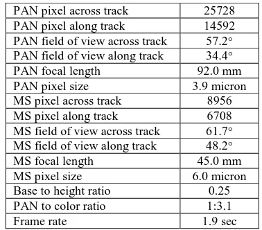
The most important camera parameters are listed in Table 1 below. The fast readout speed for the CMOS sensor provides a high frame rate which allows flying the DMC III at 150 knots speed over ground at 80% forward overlap and 6 cm GSD.
PAN pixel across track 25728 PAN pixel along track 14592 PAN field of view across track 57.2° PAN field of view along track 34.4°
PAN focal length 92.0 mm
PAN pixel size 3.9 micron
MS pixel across track 8956
MS pixel along track 6708
MS field of view across track 61.7° MS field of view along track 48.2°
Table 1 DMC III camera specification
4. TEST FLIGHT RESULTS
To finish the DMC III development project and in preparation of the first customer deliveries a series of test flights had been executed. The camera had been flown at different altitudes over various terrains which included urban areas, rural areas, forestry and water (lakes).
It is very visible in the PAN image that the CMOS sensor has a significant lower noise, especially in dark shadow areas. Also the higher dynamic range was noticeable in the images. The higher image quality is a big improvement for manual point measurements during Aero-Triangulation, especially in dark areas. Pass points are better visible for the operator and measurements of object edges are more precise. Figure 2 shows an example for a pass point in a shadow area.
Figure 2 manual point measurement in shadow areas
The CMOS sensor does not have a higher sensitivity than CCDs but because of the higher dynamic range even slightly underexposed images capture all image details in shadow areas. This looks very promising to enhance flying time per day and flying days per year.
During the test flights it could be also verified that the CMOS sensor does not show any blooming around areas of saturated pixels.
To verify the geometric accuracy of the DMC III a test flight was executed over the test area Fredrikstad, Norway. In total 136 images had been flow lap in 8 flight lines at 14 cm GSD, 80% end lap and 64% side. The RMS of the check points had The International Archives of the Photogrammetry, Remote Sensing and Spatial Information Sciences, Volume XLI-B1, 2016
XXIII ISPRS Congress, 12–19 July 2016, Prague, Czech Republic
This contribution has been peer-reviewed.
been 0.4 of a pixel for X, Y and 0.7 of a pixel for Z which even exceeded the high geometric accuracy we had achieved with DMC II.
5. CONCLUSIONS
The use of CMOS imaging sensor technology for aerial cameras provides new possibilities for systems vendors and users. It had been proven that the image quality of an aerial camera using CMOS sensors is better compared to cameras using CCDs. Especially the higher dynamic range allows to capture more information in dark areas or at lower light conditions. The significant lower noise in images generated with CMOS sensors is an advantage for feature collection and stereo mapping. Features can be seen more clearly and can be measures more precisely. These advantages can also be used to enlarge the operating envelop of the camera and to fly more hours per day and more days per year and still producing good quality image data.
REFERENCESS
Fossum, E. , 2008, CMOS Active Pixel Image Sensors: Past, Present, and Future
Sony Corporation, 2011, Advantage of the CMOS Sensor
Welzenbach, M., 2015 CMOS & CCD in Airborne Image Sensors, presentation at the ifP, Univeristy of Stuttgart
The International Archives of the Photogrammetry, Remote Sensing and Spatial Information Sciences, Volume XLI-B1, 2016 XXIII ISPRS Congress, 12–19 July 2016, Prague, Czech Republic
This contribution has been peer-reviewed.