Power MOSFET
FEATURES
• Dynamic dV/dt Rating
• Repetitive Avalanche Rated
• Isolated Central Mounting Hole
• Fast Switching
• Ease of Paralleling
• Simple Drive Requirements
• Lead (Pb)-free Available
DESCRIPTION
Third generation Power MOSFETs from Vishay provide the
designer with the best combination of fast switching,
ruggedized device design, low on-resistance and
cost-effectiveness.
The TO-247 package is preferred for commercial-industrial
applications where higher power levels preclude the use of
TO-220 devices. The TO-247 is similar but superior to the
earlier TO-218 package because its isolated mounting hole.
It also provides greater creepage distances between pins to
meet the requirements of most safety specifications.
Notes
a. Repetitive rating; pulse width limited by maximum junction temperature (see fig. 11). b. VDD = 50 V, starting TJ = 25 °C, L = 4.3 mH, RG = 25 Ω, IAS = 20 A (see fig. 12). c. ISD≤ 20 A, dI/dt ≤ 160 A/µs, VDD≤ VDS, TJ≤ 150 °C.
PRODUCT SUMMARY
VDS (V) 500
RDS(on) (Ω) VGS = 10 V 0.27
Qg (Max.) (nC) 210
Qgs (nC) 29
Qgd (nC) 110
Configuration Single
N-Channel MOSFET G
D
S TO-247
GD
S
Available
RoHS*
COMPLIANT
ORDERING INFORMATION
Package TO-247
Lead (Pb)-free IRFP460PbF
SiHFP460-E3
SnPb IRFP460
SiHFP460
ABSOLUTE MAXIMUM RATINGS
T
C= 25 °C, unless otherwise noted
PARAMETER SYMBOL LIMIT UNIT
Drain-Source Voltage VDS 500
V
Gate-Source Voltage VGS ± 20
Continuous Drain Current VGS at 10 V
TC = 25 °C
ID
20
A
TC = 100 °C 13
Pulsed Drain Currenta I
DM 80
Linear Derating Factor 2.2 W/°C
Single Pulse Avalanche Energyb E
AS 960 mJ
Repetitive Avalanche Currenta I
AR 20 A
Repetitive Avalanche Energya E
AR 28 mJ
Maximum Power Dissipation TC = 25 °C PD 280 W
Peak Diode Recovery dV/dtc dV/dt 3.5 V/ns
Operating Junction and Storage Temperature Range TJ, Tstg - 55 to + 150 °C
Soldering Recommendations (Peak Temperature) for 10 s 300d
Mounting Torque 6-32 or M3 screw 10 lbf · in
THERMAL RESISTANCE RATINGS
PARAMETER SYMBOL TYP. MAX. UNIT
Maximum Junction-to-Ambient RthJA - 40
°C/W
Case-to-Sink, Flat, Greased Surface RthCS 0.24
-Maximum Junction-to-Case (Drain) RthJC - 0.45
SPECIFICATIONS
T
J= 25 °C, unless otherwise noted
PARAMETER SYMBOL TEST CONDITIONS MIN. TYP. MAX. UNIT
Static
Drain-Source Breakdown Voltage VDS VGS = 0 V, ID = 250 µA 500 - - V VDS Temperature Coefficient ΔVDS/TJ Reference to 25 °C, ID = 1 mA - 0.63 - V/°C Gate-Source Threshold Voltage VGS(th) VDS = VGS, ID = 250 µA 2.0 - 4.0 V
Gate-Source Leakage IGSS VGS = ± 20 V - - ± 100 nA
Zero Gate Voltage Drain Current IDSS
VDS = 500 V, VGS = 0 V - - 25
µA VDS = 400 V, VGS = 0 V, TJ = 125 °C - - 250 Drain-Source On-State Resistance RDS(on) VGS = 10 V ID = 12 Ab - - 0.27 Ω
Forward Transconductance gfs VDS = 50 V, ID = 12 Ab 13 - - S
Dynamic
Input Capacitance Ciss V
GS = 0 V, VDS = 25 V, f = 1.0 MHz, see fig. 5
- 4200
-pF
Output Capacitance Coss - 870
-Reverse Transfer Capacitance Crss - 350
-Total Gate Charge Qg
VGS = 10 V ID = 20 A, Vsee fig. 6 and 13DS = 400 V b
- - 210
nC
Gate-Source Charge Qgs - - 29
Gate-Drain Charge Qgd - - 110
Turn-On Delay Time td(on)
VDD = 250 V, ID = 20 A , RG = 4.3 Ω, RD = 13 Ω, see fig. 10b
- 18
-ns
Rise Time tr - 59
-Turn-Off Delay Time td(off) - 110
-Fall Time tf - 58
-Internal Drain Inductance LD Between lead,6 mm (0.25") from package and center of die contact
- 5.0
-nH
Internal Source Inductance LS - 13
-Drain-Source Body Diode Characteristics
Continuous Source-Drain Diode Current IS
MOSFET symbol
- - 20
D
S G
TYPICAL CHARACTERISTICS
25 °C, unless otherwise noted
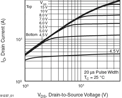
Fig. 1 - Typical Output Characteristics, TC = 25 °C
Fig. 2 - Typical Output Characteristics, TC = 150 °C
Fig. 3 - Typical Transfer Characteristics
Fig. 4 - Normalized On-Resistance vs. Temperature
VDS, Drain-to-Source Voltage (V) ID
, Dr
ain C
u
rrent (A)
20 µs Pulse Width TC = 25 °C
4.5 V 101
100
100 101
Bottom Top V15 VGS
10 V 8.0 V 7.0 V 6.0 V 5.5 V 5.0 V 4.5 V
91237_01
4.5 V
Bottom Top
VGS
15 V 10 V 8.0 V 7.0 V 6.0 V 5.5 V 5.0 V 4.5 V
20 µs Pulse Width TC = 150 °C
101
100
100 101
ID
, Dr
ain C
u
rrent (A)
91237_02 VDS, Drain-to-Source Voltage (V)
91237_03
25 °C 150 °C
20 µs Pulse Width VDS = 50 V
101
100
ID
, Dr
ain C
u
rrent (A)
VGS, Gate-to-Source Voltage (V)
5 6 7 8 9 10
4
91237_04
ID= 20 A
VGS= 10 V 3.5
0.0 0.5 1.0 1.5 2.0 2.5
- 60 - 40 - 20 0 20 40 60 80 100 120 140 160
TJ, Junction Temperature (°C) RDS(on)
, Dr
ain-to-So
u
rce On Resistance
(
N
or
maliz
ed)
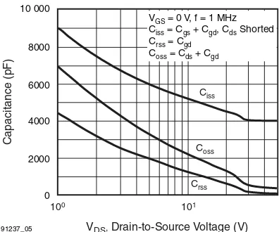
Fig. 5 - Typical Capacitance vs. Drain-to-Source Voltage
Fig. 6 - Typical Gate Charge vs. Gate-to-Source Voltage
Fig. 7 - Typical Source-Drain Diode Forward Voltage
Fig. 8 - Maximum Safe Operating Area 91237_05
10 000
8000
6000
4000
0 2000
100 101
Capacitance (pF)
VDS, Drain-to-Source Voltage (V) Ciss
Crss
Coss
VGS = 0 V, f = 1 MHz
Ciss = Cgs + Cgd, Cds Shorted
Crss = Cgd
Coss = Cds + Cgd
91237_06
ID = 20 A
VDS = 250 V
For test circuit see figure 13 VDS = 100 V
VDS = 400 V
QG, Total Gate Charge (nC) VGS
, Gate-to-So
u
rce
V
oltage (
V
)
20
16
12
8
0 4
0 40 80 120 160 200
91237_07 102
VSD, Source-to-Drain Voltage (V) ISD
, Re
v
erse Dr
ain C
u
rrent (A)
0.6 0.8 1.0 1.2 1.4 1.6 25 °C
150 °C
VGS= 0 V
101
1.8 2.0
91237_08
10 µs
100 µs
1 ms
10 ms
Operation in this area limited by RDS(on)
TC = 25 °C TJ = 150 °C
Single Pulse ID
, Dr
ain C
u
rrent (A)
103
2 5 2 5 2 5
VDS, Drain-to-Source Voltage (V) 1 2 5 10 2 5 102 2 5 103
Fig. 9 - Maximum Drain Current vs. Case Temperature
Fig. 10a - Switching Time Test Circuit
Fig. 10b - Switching Time Waveforms
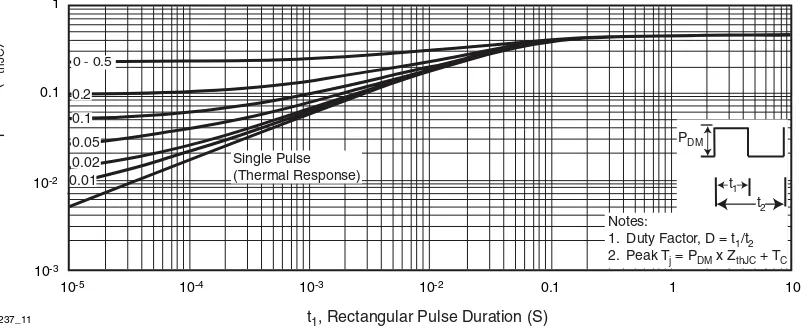
Fig. 11a - Maximum Effective Transient Thermal Impedance, Junction-to-Case ID
, Dr
ain C
u
rrent (A)
TC, Case Temperature (°C)
0 8 12 16 20
25 50 75 100 125 150
4
91237_09
Pulse width ≤ 1 µs Duty factor ≤ 0.1 %
RD
VGS
RG
D.U.T.
10 V
+ -VDS
VDD
VDS
90 %
10 % VGS
td(on) tr td(off) tf
91237_11
0 - 0.5
0.2
0.1
0.05
0.01
Single Pulse (Thermal Response)
PDM
t1
t2 Notes:
1. Duty Factor, D = t1/t2
2. Peak Tj = PDM x ZthJC + TC 0.02
Ther
mal Response (Z
th
JC
)
1
0.1
10-3
t1, Rectangular Pulse Duration (S)
10-5 10-4 10-3 10-2 0.1 1 10
10-2
RG
IAS
0.01 Ω tp
D.U.T L VDS
+ -VDD
A
10 VVary tp to obtain required IAS
IAS
VDS
VDD VDS
Fig. 12c - Maximum Avalanche Energy vs. Drain Current
Fig. 13a - Basic Gate Charge Waveform 91237_12c
Bottom Top
ID 8.9 A 13 A 20 A
VDD = 50 V
2400
0 400 800 1200 1600 2000
25 50 75 100 125 150
Starting TJ, Junction Temperature (°C)
EAS
, Single P
u
lse Energy (mJ)
QGS QGD
QG
VG
Charge 10 V
Fig. 14 - For N-Channel
Vishay Siliconix maintains worldwide manufacturing capability. Products may be manufactured at one of several qualified locations. Reliability data for Silicon
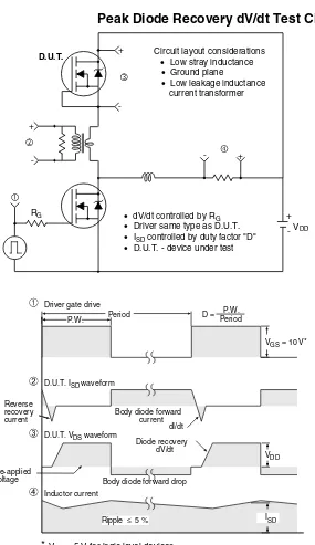
P.W. Period
dI/dt
Diode recovery
dV/dt
Ripple≤5 %
Body diode forward drop
Re-applied
voltage
Reverse
recovery
current
Body diode forward
current
VGS = 10 V*
VDD
ISD
Driver gate drive
D.U.T. ISDwaveform
D.U.T. VDSwaveform
Inductor current
D = P.W.
Period
+
-+
+
+
-*
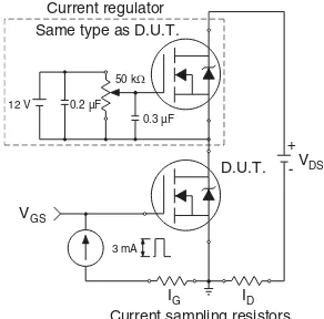
VGS = 5 V for logic level devicesPeak Diode Recovery dV/dt Test Circuit
VDD • dV/dt controlled by RG
• Driver same type as D.U.T. • ISD controlled by duty factor "D" • D.U.T. - device under test
D.U.T. Circuit layout considerations
• Low stray inductance • Ground plane
• Low leakage inductance current transformer
TO-247AC (High Voltage)
Notes
1. Dimensioning and tolerancing per ASME Y14.5M-1994.
MILLIMETERS INCHES MILLIMETERS INCHES
DIM. MIN. MAX. MIN. MAX. DIM. MIN. MAX. MIN. MAX.
A 4.58 5.31 0.180 0.209 D2 0.51 1.30 0.020 0.051
A1 2.21 2.59 0.087 0.102 E 15.29 15.87 0.602 0.625
A2 1.17 2.49 0.046 0.098 E1 13.72 - 0.540
-b 0.99 1.40 0.039 0.055 e 5.46 BSC 0.215 BSC
b1 0.99 1.35 0.039 0.053 Ø k 0.254 0.010
b2 1.53 2.39 0.060 0.094 L 14.20 16.25 0.559 0.640
b3 1.65 2.37 0.065 0.093 L1 3.71 4.29 0.146 0.169
b4 2.42 3.43 0.095 0.135 N 7.62 BSC 0.300 BSC
b5 2.59 3.38 0.102 0.133 Ø P 3.51 3.66 0.138 0.144
c 0.38 0.86 0.015 0.034 Ø P1 - 7.39 - 0.291
c1 0.38 0.76 0.015 0.030 Q 5.31 5.69 0.209 0.224
D 19.71 20.82 0.776 0.820 R 4.52 5.49 0.178 0.216
D1 13.08 - 0.515 - S 5.51 BSC 0.217 BSC
ECN: X13-0103-Rev. D, 01-Jul-13 DWG: 5971
0.10MCAM
E E/2
(2)
(4) R/2
B
2 x R
S
D
See view B
2 x e b4
3 x b 2 x b2
L C
L1
1 2 3
Q
D A
A2 A
A
A1 C
Ø kMDBM
A
ØP (Datum B)
ØP1
D1
4
E1
0.01MDBM
View A - A Thermal pad
D2
D D E E
C C
View B
(b1, b3, b5)
Base metal
c1
(b, b2, b4)
Section C - C, D - D, E - E (c)
Planting 4
3
5
7
4
4 4
Lead Assignments 1. Gate
Disclaimer
ALL PRODUCT, PRODUCT SPECIFICATIONS AND DATA ARE SUBJECT TO CHANGE WITHOUT NOTICE TO IMPROVE
RELIABILITY, FUNCTION OR DESIGN OR OTHERWISE.
Vishay Intertechnology, Inc., its affiliates, agents, and employees, and all persons acting on its or their behalf (collectively,
“Vishay”), disclaim any and all liability for any errors, inaccuracies or incompleteness contained in any datasheet or in any other
disclosure relating to any product.
Vishay makes no warranty, representation or guarantee regarding the suitability of the products for any particular purpose or
the continuing production of any product. To the maximum extent permitted by applicable law, Vishay disclaims (i) any and all
liability arising out of the application or use of any product, (ii) any and all liability, including without limitation special,
consequential or incidental damages, and (iii) any and all implied warranties, including warranties of fitness for particular
purpose, non-infringement and merchantability.
Statements regarding the suitability of products for certain types of applications are based on Vishay’s knowledge of
typical requirements that are often placed on Vishay products in generic applications. Such statements are not binding
statements about the suitability of products for a particular application. It is the customer’s responsibility to validate that a
particular product with the properties described in the product specification is suitable for use in a particular application.
Parameters provided in datasheets and / or specifications may vary in different applications and performance may vary over
time. All operating parameters, including typical parameters, must be validated for each customer application by the customer’s
technical experts. Product specifications do not expand or otherwise modify Vishay’s terms and conditions of purchase,
including but not limited to the warranty expressed therein.
Except as expressly indicated in writing, Vishay products are not designed for use in medical, life-saving, or life-sustaining
applications or for any other application in which the failure of the Vishay product could result in personal injury or death.
Customers using or selling Vishay products not expressly indicated for use in such applications do so at their own risk.
Please contact authorized Vishay personnel to obtain written terms and conditions regarding products designed for
such applications.