Fabrication of Solution-Processed Methylammonium Lead Iodide
PerovskiteSolar Cells and Photodetector
To cite this article: Diana A. Barus et al 2018 J. Phys.: Conf. Ser.1116 032005
View the article online for updates and enhancements.
Fabrication of Solution-Processed Methylammonium Lead
Iodide PerovskiteSolar Cells and Photodetector
Diana A. Barus*, Kerista Sebayang, Junedi Ginting, Riski Titian Ginting
Department of Physics, Faculty of Mathematics and Natural Science, University of Sumatera Utara, Medan, Indonesia, 20155
*Email: [email protected]
Abstract. Perovskite based on methylammonium lead iodide (MAPbI3) have attracted great attention for the past few years as promising materials for both photovoltaics and photodetector technologies. In this work, we report on the solution-processed of MAPbI3 via spin-coating method prepared at high humidity condition. The compact film of MAPbI3 with grain size of 200 nm and high crystallinity was obtained. Based on the current density –voltage (J-V) measurement, relatively high power conversion efficiency of 11.3% of PSCs can be achieved when processing the MAPbI3 film at high humidity. In addition, the calculated detectivity and responsivity of perovskite photodetector can reached up to 2 A W-1 and 2 x 10¹² Jones at wavelength of 500 nm with rapid response time of 2 ms.This finding shows that MAPbI3 processed at high humidity can achieve both high photovoltaic and photodetector performance.
1. Introduction
For the past few years, methylammonium lead iodide (MAPbI3) have attracted a lot of attention due to its unique properties such as balanced electron and hole mobilities, tunable optical band gap, low temperature processing, solution-processed and large diffusion length [1-2].MAPbI3 in the field of photovoltaics demonstrates rapid improvement for only 6 years of research with the efficiency higher than 22% from 3.8% [3-4]. However, relatively less investigation of MAPbI3 as photoactive layer in photodetectors research field. There is several type of perovskite based photodetector such as photodiode, photoconductor (metal-semiconductor contact) and phototransistor. The advantages of photodiode compared to other type of photodetector is that it demonstrates low noise current, high detectivity (D*) and etc. Most of the research focusing on the GaN, Si, ZnO, and organic based photodetector [5]. However, it suffered from the slow response, where recent development require rapid light detection time. In this work, using similar device structure of solar cells type (p-i-n structure), the photodetector performance was investigated.
2
transport layer, and Ag as top electrode (cathode). The surface morphology, crystallinity, photovoltaic and photodetector performance were investigated. Based on our finding, the solution-processed PSCs show relatively high photovoltaics and photodetectors performance.
2. Methodology
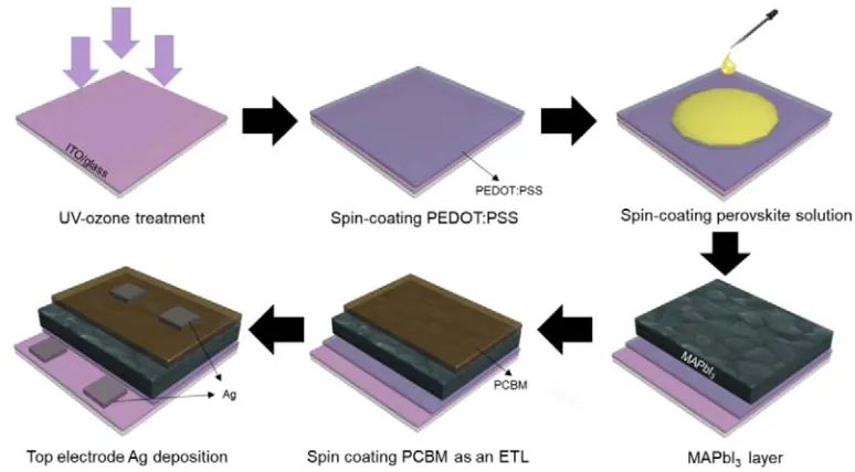
First, ITO/glass substrate was ultrasonically clean with acetone, ethanol and isopropanol in sequence for 10 min each and drying in oven for overnight. Prior to spin coating PEDOT:PSS (P VP AI 4083, Clevios) layer at 5,000 rpm for 30 s, ITO substrate was UV-ozone treated to remove the impurities. After PEDOT:PSS coating, the substrates was annealed at 150 oC for 10 min. The perovskite film was prepared based on previous report to form a thickness of 300 nm at humidity of 70 %. The sample was then baked at 100oC for 10 min for high crystallinity. Subsequently, the sample was transferred into N
2 glove box. The PCBM with concentration of 20 mg/ml was prepared in chlorobenzene solution and stirred for 24 h prior to use. 40 µL of PCBM was then spin-casted at 1,500 rpm for 30 s. Without further annealing, 100 nm of Ag top electrode was thermally deposited with an active area of 9 mm2. Figure 1 displays the schematic illustration of perovskite based solar cells and photodetectors fabrication process.
Field emission scanning microscope electron (FESEM) images of MAPbI3 were carried out using a Hitachi S-4800. Current density – voltage (J–V) curves of PSCs was evaluated using a Keithley 2400 SMU under simulated AM 1.5G illumination of 100 mWcm-2by Oriel Sol 1A (Newport). The external quantum efficiency, responsivity, and detectivity were measured by a monochromator Acton SpectraPro (Princeton instrument) equipped with 300 W of Xe lamp as a light source, where Si photodetector was connected with multi-function power meter Newport 1835 C to determine the input power (Pin) of monochromatic light. For photoresponse measurement, an optical chopper was used to modulate the on and off light switching and the data was recorded by oscilloscope 300 MHz (Siglent).
3. Results and Discussion
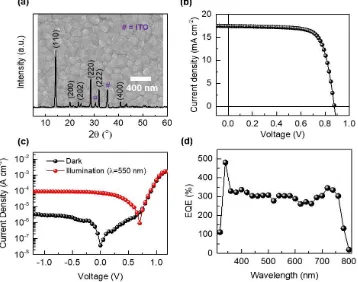
Figure 2a shows the X-ray diffraction (XRD) patterns of perovskite MAPbI3 on ITO/PEDOT:PSS surface which prepared at high humidity condition. Based on the peaks position at 14.1o, 20.0o, 23.50o, 28.5o, 31.9o and 40.7o corresponding to the (110), (200), (202), (220), (222) and (400) peaks, which can be assigned to the tetragonal MAPbI3 lattice, indicates pure crystallinity phase without the PbI2 impurities peak. The surface morphology of MAPbI3 shows compact and uniform films when deposited on top of ITO/PEDOT:PSS substrate with an average grain size of 200 nm (pinhole free formation). The J-V characteristics of PSCs were measured under AM 1.5G with illumination of 100 mW cm-2 measured using the shadow mask of 9 mm2 as shown in Figure 2b. The short circuit current density (Jsc) of 17.45 mA cm-2, open circuit voltage (Voc) of 0.88 V, fill factor (FF) of 74 %, leading to power conversion efficiency (PCE) of 11.3 % as summarized in Table 1. Based on Figure 2b, the series (Rs) and shunt resistance (Rsh) can be determine of 55 and 21 x103Ωcm2, respectively.
4
Table 1. Summary of photovoltaic parameters and photodetectors based on MAPbI3 photoactive layer.
Sample Jsc
Figure. 2c depicts the J-V characteristics of the perovskite photodetector (ITO/PEDOT: PSS/MAPbI3/PCBM/Ag) device under dark and light illumination of 550 nm with power density of 78 µW cm-2. The dark current shows at 2.2 µA cm-2 at -0.5 V and the photocurrent increased by two order of magnitude to 114 µA cm-2, resulting on/off photocurrent ratio of 51. The external quantum efficiency (EQE) was calculated based on the expression [6]: EQE =[(Ip/q)/(Pop/hv)], Ip represent photocurrent, q is elementary charge, Pop is light intensity and h is planck’s constant. Figure 2d shows the high EQE from spectral range of 300 to 800 nm represents wide detection from UV to near infra-red. The responsivity (R) and detectivity (D*) of perovskite photodetector was calculated based on the following equation, where Jph is photocurrent density, Plight represents monochromatic light intensity (78 µW cm-2) and Jd correspond to dark current density [7]:
=
(1) ∗=
(2)
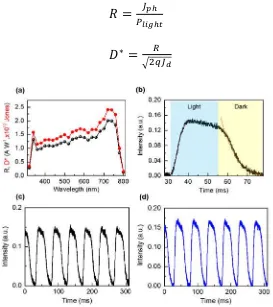
Based on the above calculation, Figure 3a depicts the R and D* of perovskite photodetector at 550 nm of 1.3 A W-1 and 1.6 cm Hz0.5W-1, respectively where 1 cm Hz0.5W-1 is equivalent to 1 Jones. Our findings shows that the responsivity five times higher than the polymer based photodector of 0.25 A W-1[7] owing to the low recombination rates. The photoresponse is critical parameters to understand the optoelectronics device. Figure 3b shows the intensity of light and off detection as function of time at 550 nm, where the rise and fall time was calculated of 5 and 7 ms. Figure 3c and d shows the reproducible and stable photoresponse (on/off) cycles when illuminated at 550 and 720 nm, which implies an excellent light-switching of perovskite photodetector even without any bias voltage applied on the device. Interestingly, we found that at 720 nm, the photoresponse intensity is higher compared to 550 nm due to strong absorption of perovskite at near-infrared region.
4. Conclusions
In conclusion, we have successfully demonstrated the solution-processed perovskite solar cells and photodetector prepared at high humidity condition. The ITO/PEDOT:PSS/MAPbI3/PCBM/Ag device structure shows device efficiency as high as 11.3 %, based on uniform and large grain size of MAPbI3 (pinhole free). The high responsivity of 1.3 A W-1, high detectivity of 1.6 x 10¹² Jones and rapid response time of 5/7 ms (at 0 V) was achieved for MAPbI3photodetector, which shows higher performance than the previous photodetector based on polymer. Our findings demonstrate high photovoltaic and photodetector performance and cost effective MAPbI3 processing at ambient air.
5. Acknowledgements
The authors would like to thank University of Sumatera Utara (USU–Medan) Ministry of Research, Technology and Higher Education of Indonesia for Financial support in this work.
References
[1] Liu, M., M.B. Johnston, and H.J. Snaith 2013 Nature 501 395
[2] Yang, W.S., J.H. Noh, N.J. Jeon, Y.C. Kim, S. Ryu, J. Seo, and S.I. Seok 2015 Science 348 1234 [3] Kojima, A., K. Teshima, Y. Shirai, and T. Miyasaka. 2009 Journal of the American Chemical
Society 131 6050