T he aim of this international project is to develop a smart hybrid gas multi-sensor module for environmental applications, i.e. by combining thick-film, thin-film and polymer-film sensor elements with a signal processing ASIC within a single package, which should be useful for all sensor types. T he module should enable multi-sensor operation as well, when connected to an intelligent signal-processing unit. T he sensor module has a number of advantages including the possibility of minimising temperature, humidity and gas compound interference effects. T he ASIC converts the sensor resistance into an industrial standard current signal (4-20mA), which makes the smart sensor module easier to use in industrial environments. T he main compo-nents of the module also determine the design directions as follows:
• the ASIC chip;
• the sensor resistor elements; and • the package.
1. Syst em concept
T he block diagram of the intelligent gas sens-ing measurement set-up is illustrated in Figure 1. T he ASIC involved here has the aim of converting the resistivity changes (most likely within the range of 102-105Ω) of the gas sensor elements into an electrical signal. T his is a 4-20mA current loop signal, which avoids the influence of connecting cable resistance values. T he sensor resistor element is compared with a reference resistor to compensate for some undesired environment effects, such as temper-ature fluctuations. T his is obtained by exposing the reference resistor to the same environment, but isolating it from the effect of gas(es). T he ASIC contains a preamplifier, a low pass filter and a voltage-to-current (V-I) converter. To provide the widest flexibility, and uniform packaging and electrical connections for sensor elements of different nature, the following system assembly considerations were met: • sensor modules will be packed individually
in the first approach;
Sensor Review
Volume 19 · Number 2 · 1999 · pp. 128–134 © M CB University Press · ISSN 0260-2288
Com bining inorga nic
a nd orga nic ga s se nsors
e le m e nt s: a ne w
a pproa ch f or m ult
i-com pone nt se nsing
G. H arsányi, M . Réczey,
R. Dobay, I. Lepsényi,
Zs. Illyefalvi-V itéz ,
J. Van den S teen, A . Vervaet,
W. Reinert, J. Urbancik,
A . Guljajev, Cs. V isy, Gy. Inzelt and
I. Bársony
The authors
G. Harsányi, M . Réczey, R. Dobay, I. Lepsényi and
Zs. Illyefalvi-Vitézare all at the Technical University of Budapest, Department of Electronics Technology, Budapest, Hungary. Tel: + 36 1463 3634; Fax: + 36 1463 4118; E-mail:
J. Van den Steen and A. Vervaetare at IM EC, Belgium. W. Reinertis at CEM , Germany.
J. Urbancikis at TU Kosice, Slovakia. A. Guljajevis at M PEI, Russia. Cs. Visyis at JATE, Hungary. Gy. Inzeltis at ELTE, Hungary. I. Bársonyis at M icrosensor, Hungary.
Keyw ords
Gas sensors, M ulti-sensor systems, Sensors
Abstract
Atmospheric dependent, gas sensitive resistors seem to be good candidates for detecting critical air pollution levels. Recently, great progress has been made in the development of various sensor types, but less attention seems to be paid to the integra-tion of sensor elements w ith different characteristics. The aim of this international project is to develop a smart hybrid gas multi-sensor module for environmental applications, i.e. by combining classical thick- and thin-film elements w ith polymer-film based sensors and also a signal processing ASIC w ithin a single package, w hich should be useful for all sensor types. The module should enable multi-sensor operation as w ell, w hen connected to an intelligent signal-processing unit.
Electronic access
The research register for this journal is available at ht t p://w w w 2.m cb.co.uk /m cbrr/sr.a sp
The current issue and full text archive of this journal is available at ht t p://w w w .e m e ra ld-libra ry.com
• a single module contains the following elements: one gas sensor with one refer-ence resistor, one signal conditioner ASIC , and an optional heating supply circuit where necessary;
• an array of such modules will be built up by fixing them on a motherboard and
connecting them to the data transmission, multiplexing and data acquisition units; • intelligent functions are added from
outside of the modules;
• the ASIC may also contain some multi-plexing capability for future extension purposes, enabling the integration of sensor arrays inside the same module.
2. ASIC design
A 2µm-resolution H BIM O S technology has been selected for the design of the ASIC (available at Alcatel M ietec). T his technology is aimed at the automotive market and there-fore offers a combination of M O SF ET, bipolar and D M O S devices with voltage ranges from 5 to 100V. T he M O SF ET S can operate up to 15V and are particularly useful for our purposes as they combine small size and sufficient voltage range.
T he circuit proposed here is a folded version of the classic bridge, followed by a V-I converter. One of the advantages is that the voltage signal is proportional to the ratio of the reference resistor and the sensing resistor. T he core of the ASIC is the design of a M OS opera-tional amplifier. T he amplifiers used only have to cope with low frequency signals, so that bandwidth is of less concern. T he operational amplifier circuit layout is based on a design described in Eynde et al. [1]. T he circuit topology chosen allows high linearity and high output current. T his operational amplifier features an AB output stage to guarantee
linearity and to drive the relatively important resistive loads. T he operational amplifier has a pull-down feature, allowing different ampli-fiers to be driven from the same output pad; the pull-down feature forces the output to become high impedance by pulling the gates of the output transistors to their respective source voltages. T his can be used for reducing power consumption, but also for multiplexing the outputs of several operational amplifiers, allowing arrays of sensors to be connected to a single ASIC (single signal output). At the layout level, several blocks are common to the different signal conditioners; e.g. the bias circuit and reference sources are common to all amplifiers. F urthermore, as only one of the output V-I converters should be operating at the same time, silicon area can be saved by multiplexing the outputs of the intermediate “voltage adjusting” amplifiers to a single V-I converter block. T he amplifier supply voltages are –6v and + 6v, with an output voltage range between –5v and + 5v. T he common mode input range must fit these data as operational amplifiers are used in cascade: both a p and n differential input pair are used to accommo-date this requirement.
Simulations show an operational tempera-ture range of 0 to 80°C . T he ASIC must feature temperature invariability as the heated gas sensors and ASIC are intended to be assembled into a single package.
3. Gas sensor resist or research
G as sensor resistor array research and develop-ment is being undertaken in three directions at three different research centres in order to get a wide variety of behaviour and also a number of possible gas compounds to be monitored. T he main sensor element types should be based on the following technologies and materials: • thin-film SnO2resistor elements operated
at high temperatures;
• thick-film SnO2resistor elements prepared from organo-metallic pastes and operated at high temperatures;
• electroactive conducting polymers (EC Ps) deposited electrochemically or chemically on thick-film substrates operated at room temperatures.
A common property of all three types is that the sensor elements are resistors. T hey can be used to sense gases and vapours by monitoring
Signal conditioner
4-20 mA current trans mis s ion
Sens or
Smart s ens or
Data trans mis s ion
I – V
the changes in conductance on exposure of the films to the gas sample.
3. 1 Thin polycrystalline S nO2fi lm gas sensors
Over the past few decades, solid-state gas sensors based on SnO2have become the pre-dominant solid-state devices for gas alarms used in domestic, commercial and industrial premises[2,3]. Even sensor arrays have been fabricated using exclusively inorganic materials of the same nature [4]. T he detailed analysis of the extensive literature is out of scope here, although we give some new references [2-6].
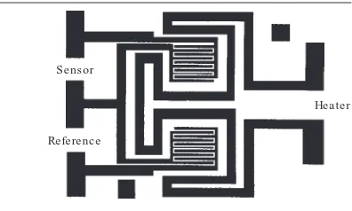
T he original construction of the thin film gas sensors proposed in this work is shown in F igure 2. It consists of two resistors with interdigital finger structures, having three contacts: one contact of the two resistors is common. T he heater meander surrounds both elements to provide equal temperature for them. A thin SnO2film is deposited onto the surface of the substrate over the interdigi-tal electrodes and ought not to cover the heater. Such a structure permits the device to work as a differential sensor when a protective dielectric film (SiO2, Al2O3, and M gF ) covers one of the two resistors for reference purposes, or it is doped with some impurities for varying the selectivity.
T he contacts and the heater were fabricat-ed from a vacuum evaporatfabricat-ed C r bottom adhesion promoter layer and a sputtered Pt on the surface of 25 × 25-mm-area mica or quartz substrates. T he thickness of the mica substrate was about 80-120µm and that of the quartz was 200µm. T he sensor structure has a size of 12.5 × 12.5mm. So one substrate includes four sensor elements. T he sensor pattern was formed by photolithography.
SnO2thin films were prepared by reactive sputtering from a pure tin target (99.99 per cent) in an atmosphere of 88 per cent Ar / 12
per cent O2. T he deposition of the films was conducted through a stainless steel mask. T he temperature of the substrates during the deposition of SnO2films was 400°C .
3. 2 Thick- fi lm organo- m etallic resistor elem ents
SnO2based sensors can also be fabricated by standard thick-film technology using organo-metallic pastes that provide the raw material of the resistor through chemical decomposition-oxidation processes during firing. Since the sensor elements have working temperatures at about 450°C , a careful selection of materials is necessary in order to produce a system with long-term reliable operation without drifts due to ageing. T he design of the sensor could be split into two main tasks: the first problem represents the design of the sensorial part and the second poses the sensor heater resistor.
T he principle of gas sensing is based on reversible molecular interactions on the active surface of SnO2. T his is why the specific surface, i.e. the ratio of effective surface and film volume could be minimised. T hick-film technology for sensor production can not fully respect this demand. T his fact could cause increased interference reactions in compari-son with thin film sensors.
T he model of gas sensing mechanism in grainy semiconductor thick-film SnO2layers is well described in the technical literature [7,8]. T he adsorbed oxygen molecules remove conduction electrons from the grain boundaries, thin depletion layers are created on the surface of the grains. T he energy barri-er between the grains is modulated if a com-bustible gas compound removes oxygen ions from the surfaces. T he result will be a measur-able resistance variation.
C hemical compounds, like Pt or Pd may catalyse the gas sensing by two major mecha-nisms: concentrating reaction constituents onto the active surface and decreasing the level of activation energy by influencing the Fermi energy level inside the semiconduc-tor[6]. It is obvious that the exact preparation of raw materials for the sensor layer has a determining influence on the sensor’s behav-iour. Sensor arrays have already been fabricat-ed mainly by two approaches: varying addi-tives or operating temperature of sintered thick-film tin-dioxide resistor elements[9].
D esign of the sensorial part is based on the idea that both surfaces of a sensor substrate will be used: top side for the sensing part, and back
Sens or
Reference
Heater
side for the heating element. T he idea to collo-cate both parts on the one side of the substrate is unsuitable for manufacture using standard thick film technology. T he layout of the sensor-ial part is shown in Figure 3(a). T he resistance of the SnO2layer is measured between inter-digital Au electrodes. Two elements are realised: one for the sensor and the other for the reference resistor. T he latter one is covered by a film to prevent reactions with gas com-pounds.
G enerally, the heater has an important effect on gas sensors because the working temperature is relatively high, and its distribu-tion on the substrate surface must provide equal temperature for the overall sensor and reference resistor film. T he heating element is placed onto the backside of the sensor sub-strate. T hermal modelling was used to optimise its structure which is illustrated by F igure 3(b). O ne simple solution is to apply a number of thick film thermistor resistors connected in parallel. T he eventual result of this design is drawn in the F igure: it repre-sents one conductive layer with interdigital structure and a simple resistive layer, which generates the demanded system of parallel resistors in this layout.
3. 3 Conducting polym er fi lm based sensors
At the beginning of the 1980s, the ultimate property of most polymers, which distinguishes them from metals, was their inability to carry electricity. Electrical conductivity was intro-duced into these materials by adding conduc-tive grains to form a metal/polymer composite, or by the incorporation of ionic species to form polymer electrolytes. D uring the past 20 years, a new group of organic polymers has been revealed with the ability to conduct electrical current inherently. T hese electroactive-conducting plastics (EC Ps) are still under development for appropriate applications, such
as rechargeable batteries, capacitors, field-effect transistors, enzymatic biosensors, and gas sensors. T hey may offer a number of advantages over conventional inorganic based sensors. Because of their very unique and specific behaviour, they are considered intelli-gent material systems. T he aim of the research in the frame of this international project is to find a practical exploitation of the special properties of these type of materials by completing the system of inorganic gas sensor resistor materials with EC Ps and thus intro-ducing new potential possibilities into the targeted intelligent gas monitoring system.
EC Ps can easily be synthesised and deposited onto conducting surfaces by a simple electrochemical polymerisation method, where the doping reaction modulates the conductivity reversibly via redox inter-actions. Electroconducting conjugated poly-mers are good candidates for the elaboration of chemical or electrochemical sensors in two ways: either as a matrix for immobilisation of active compounds or as sensitive components, where some properties of the polymer film changes in presence of the studied phenome-na. T he electronic conductivity related to the doping level of an EC P is modulated by the interaction with various substrates and analytes. T he incorporated doping ions or other species transmit film and environmental interactions.
A variety of devices have been developed and constructed utilising the reversibility in redox properties of EC P films, coupled with the incorporation of electrolyte anions into the polymer film, and dissolution of them which may take place in the redox reaction. T herefore, conducting polymers can also be used to sense gases and vapours by monitor-ing the change in conductance on exposure of the polymer to the sample gas. Preliminary studies on these materials have shown that they exhibit a fast and reversible response even at room temperatures, which can not be
A B C A B
(a) (b)
Figure 3 Layout build-up of the thick-film gas sensor: (a) topside w ith the sensor and reference resistors (A-conductor,
expected with inorganic films [10,11]. T hese polymers have a number of distinct advan-tages in the point of view of gas sensing: • a wide variety of polymer materials is
available;
• they can be formed by electrochemical polymerisation of the monomer under coulombmetrically controlled conditions; • a number of doping materials can be
incor-porated;
• the thickness of the film is variable by changing the polymerisation time; • the gas sensors should operate at room or
close room temperatures;
• they are cheap enough to provide dispos-able sensor elements.
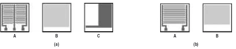
One disadvantage of these materials is their lack of specificity: they show responses to a wide range of different gases and vapours. Lots of EC Ps were studied for use in gas sensors. T hey produce non-selective response to differ-ent gases[12-14]. On the other hand, their selectivity behaviour seems still to be better than that of the inorganic material based gas sensitive resistors. For example, polypyrrole showed a much higher sensitivity to methanol than to ethanol, and it is also highly sensitive to nitrous gas compounds, such as N H3and N O2. T hese effects differ considerably from those found with inorganic SnO2based gas sensor resistors and give a good chance of improving the selectivity when combining organic and inorganic based sensor elements within an intelligent monitoring unit.
T he conductor film should be realised first by conventional thick-film processing, applying screen printing onto 96 per cent alumina sub-strates. Since a resistor film should be created, two conductors with an isolation gap are neces-sary for this element. Since the resistor film is electrochemically deposited, its grow-through between the electrodes should be reached to form a real resistor film. T hus, a narrow gap should be fabricated between the electrodes the resolution of which can not be realised by conventional screen printing technology. T herefore, a continuous film should be screen-printed first, and it should be divided by a gap made by laser engraving into the film. T hus, laser processing is necessary in the second main step of technology. T he last step is the electro-chemical deposition and grow-through of the polypyrrole to form a gas sensitive resistor film.
T he layout in F igure 4 had to be completed with a special interconnection system that
enabled the application of equal-potential surfaces on all the electrodes of one substrate during the electrochemical deposition. T hese auxiliary conductors and pads were removed from the sample by detaching the parts that are unnecessary for gas sensor operation. T he output pad system corresponds to the stan-dard pin arrangement. T he overall size of the rectangular-shape element is 5mm ×12mm which allows it to fit well together with a reference resistor into the window of the package shown in the following section.
3. 4 Testing gas sensitive resistors G as sensitivity behaviour of thin- and thick-film SnO2resistors have been studied for many years and are well known from the literature [2-9]. In general, the prepared samples also followed this behaviour:
• Sputtered thin-film SnO2resistors showed very good sensitivity for C O and H2, less sensitivity for hydrocarbons and alcohol vapours (operating temperature 350°C ). • T hick-film SnO2resistors are rather
sensi-tive for hydrocarbons (especially for methane) and alcohol vapours, H2, and less sensitive for C O. T heir behaviour is rather uncertain for ammonia and N Ox (operating temperature 450°C ).
• Rgas/R0characteristics are close negative linear curves in a log-log plot.
• Sensor characteristics can slightly (but not significantly) be modified with precious metal additives into the material, or by varying the operating temperature between 350 and 450°C .
• A conclusion was drawn to use twin element sensor arrays when combining different behaviours for multi-component sensing.
Conductor pad Alumina s ubs trate Las er cut
Polymer film
Figure 4 Layout design of the polymer gas sensor
Less information is available about gas sensitive EC P films[10-14]. D uring our experiments, we concluded the following:
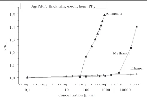
• Electrochemically and chemically deposited polypyrrole (PPy) films show good
sensitivity for ammonia, less for methanol, almost no sensitivity for ethanol, and practically no sensitivity for other compounds mentioned above (operating temperature 25°C ). T heir characteristics are given in F igure 5.
• Electrochemically deposited polyanailine (PAN i) films show extremely good sensitivity for ammonia, less for N Oxand practically no sensitivity for other compounds (operating temperature 25°C ).
• A conclusion was drawn to use twin ele-ment sensor (PPy and PAN i) arrays when combining different behaviour for the multi-component sensing.
T hus, a combination of inorganic thin- and thick-film SnO2with EC P film resistors should be a good candidate of gas sensitive resistor arrays for environmental multi-com-ponent sensing when the goal is to distinguish hydrocarbon, C O, N Oxand ammonia type pollutants while also screening out the dis-turbing cross-effects of H2and alcohols at the same time.
4. Packaging concept
Integrating sensor elements and the ASIC into the same module provides a great challenge for packaging. A number of require-ments must be met, the package must assure: • the minimal possible size for the overall
module;
• a cost effective interconnection between the sensor elements and the IC ;
• the protection of the ASIC chip from all environmental effects (gases, sensor heating, etc.);
• the minimal heat conductance between heated sensor elements and their environ-ment;
• the possible inclusion of non-heated sensor elements;
• “gas transparency” for the monitored medium towards the sensor;
• “gas isolation” of the reference elements.
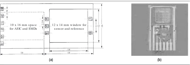
T he designed substrate for the sensor module is shown in F igure 6.
T he heated sensor elements are connected by wires to the module substrate. Polymer based sensors can directly be bonded onto the substrate. T he sensor substrate may have a maximum area of 12 × 14mm. T he contacts are gold plated to allow wire bonding. Eleven contacts are present on the substrates, five correspond to the sensor element connec-tions. T he sensorial part is closed with gas transparent stainless steel screens for mechan-ical protection. T he ASIC is wire bonded and closed with globe-top packaging. Some sur-face mounted (SM ) components are also soldered around it. T he process flow is as follows: board manufacturing; solder paste printing; pick and place of SM D s; reflow soldering; cleaning; die bond adhesive dis-pensing; die bonding of ASIC (s); curing; wire bonding; first tests; globe top dispensing; curing; bonding of the sensor; prefabricated cap mounting; testing.
5. Conclusions
T he main goal of this research is to find a new approach for multi-component gas sensing by combining a new type of organic conducting polymer based and conventional inorganic thin- and thick film metal-oxide sensor resistor elements. T he first testing of the sensor resistor elements indicated that there might be a great difference in sensor respons-es which therefore allows for the fabrication of an array of sensors for highly effective multi-component sensing. T he very different nature and operating conditions of the sensor elements needed a special concept for the array design: sensor elements are individually combined with an ASIC signal conditioner for getting compatible output signals. Packaging
Concentration [ppm]
R
/R
O
Methanol
Ethanol Ammonia
Ag/Pd/Pt Thick film, elect.chem. PPy
0,1 1 10 100 1000 10000 1,5
1,4 1,3 1,2 1,1 1,0
design must also be flexible enough to allow for uniform outlines with different sensors. All these issues have been discussed in the paper. A real multi-component sensing test now requires that we connect the smart elements into an intelligent signal processing system and this is the subject of our ongoing research.
Ref erences
1 Eynde, Op’T et al., “ A CM OS large swing low-distor-tion three-stage class AB pow er amplifier” , IEEE Journal of Solid State Circuits, Vol. 25 No. 1, February, 1990.
2 Göpel, W. and Schierbaum, K.D., “ SnO2sensors:
current status and future prospects” , Sensors and Actuators B, 26-27, 1995, pp. 1-12.
3 Schierbaum, K.D., “ Engineering of oxide surfaces and metal/oxide interfaces for chemical sensors: recent trends” , Sensors and Actuators B, 24-25, 1995, pp. 239-47.
4 Hoefer, U., Böttner, H., Fleske, A., Kühner, G., Steiner,
K. and Sulz, G., “ Thin-film SnO2sensor arrays
controlled by variation of contact potential – a suitable tool for chemometric gas mixture analysis in the TLV range” , Sensors and Actuators, 1997, pp. 429-33.
5 Baranzahi, A., Lloyd Spetz, A., Glavmo, M., Carlsson, C., Nytomt, J., Salomonsson, P., Jobson, E., Häggendal, P., Mártensson, P. and Lundström, I., “ Response of metal-oxide-silicon carbide sensors to simulated and real exhaust gases” , Sensors and Actuators, 1997, pp. 52-9.
6 Delabie, L., Honoré, M ., Lenaerts, S., Huyberechts, G., Roggen, J. and M aes, G.,“ The effect of sintering a
Pd-doping on the conversion of CO to CO2on SnO2
gas sensor materials” , Sensors and Actuators, 1997, pp. 446-51.
7 Gas Detection M echanism, in Figaro Gas Sensors, Product Catalogue, Vol. 2, p. 2.
8 Chiorino, A., Ghiotti, G., Prinetto, F., Carotta, M .C., M artinelli, G. and M erli, M ., “ Characterization of
SnO2-based gas sensors. A spectroscopic and
electrical study of thick films from commercial and laboratory-prepared samples” , Sensors and Actuators, 1997, pp. 474-82.
9 Heilig, A., Bârsan, N., Weimar, U., Schw eizer-Berberich, M ., Gardner, J.W. and Göpel, W., “ Gas indentification by modulating temperatures of
SnO2-based thick film sensors” , Sensors and
Actuators, 1997, pp. 45-51.
10 Bidan, G., “ Electroconducting conjugated polymers: new sensitive matrices to build up chemical or electro-chemical sensors. A review.” , Sensors and Actuators B, Vol. 6, 1992, pp. 45-56.
11 Charlesw orth, J.M ., Partridge, A.C. and Garrard, N., “ M echanistic studies in the interactions betw een poly(pyrrole) and organic vapors” , J. Phys. Chem., Vol. 97, 1993, pp. 5418-23.
12 Bartlett, P.N., Archer, P.B.M . and Ling-Chung, S.K., “ Conducting polymer gas sensors Part I.: Fabrication and characterization” , Sensors and Actuators, Vol. 19, 1989, pp. 125-40.
13 Bartlett, P.N. and Ling-Chung, S.K. (1989), “ Conduct-ing polymer gas sensors Part II: Response of polypyrrole to methanol vapour” , Sensors and Actuators, Vol. 19, pp. 141-50.
14 Bartlett, P.N. and Ling-Chung, S.K., “ Conducting polymer gas sensors Part III: Results for four different polymers and five different vapours” , Sensors and Actuators, Vol. 20, 1989, pp. 287-92.
10 x 16 mm s pace for ASIC and SMDs
12 x 14 mm w indow for s ens or and reference
2
.5
4
16
14 18
5 12 16
2
.5
4
(a) (b)