Time Lag in CM II E
Dielectric S
Zainuddin Nawawi .
Dept. of Electrical Engineering Sriwijaya University outdoor insulation system for high voltage appl taking into consideration the phenomena in insulation systems [1]. It has been seen that t deference between the application of a voltage cause breakdown and the occurrence of the brea This time difference is called statistical time electrical apparatus use air as the insulating mediu discharge time lag (SDTL) is very important engineering designs of high voltage apparatus an equipment. In insulation coordination especially, characteristics of different electrical apparatu importance to identify [1]. The requirement for t devices is that their volt time curve must be l withstand level of the protected insulation wit region in which the protection is intended [2]. If device for instance rod gap, the margin of the tw be adequate to allow for the effects of distan
Dept. of Electrical Engineering Tanjungpura University voltage sufficient to e breakdown itself. ]. If the protective the two curve must distance, polarity, and aging of the
insulation. SDTL test on protective deterioration such as surface erosion from the difficulty, due to the development in insulator design and formulations, the tests would be expe field investigation that may not alwa simulation testing in field conditions fo in laboratory scale may provide an al obtaining faster useful results. This pa approach, which is aimed at finding characteristics change such as SDTL surface roughness. In addition, the surfa rough and smooth insulation surface ha An artificial small size of gap has been using the CM II electrode system [3 concluded that SDTL has been affecte insulation surface in which the void w some new results have been added in give better explanation.
II. EXPERIMEN
The employed specimen was th electrode system. One side of the flat g a metallic electrode, and the other side
of Electr.& Electron.Engg. oyohashi University of Tech.
Toyohashi, Japan [email protected]
ective devices subjected to osion in real situation suffer the continuously ongoing n and use of new material s been successfully employed
3]. In that paper, it was e flat gap was in contact with her side with insulation. The plate of PMMA, as shown in
Specimens
D-50 2012 IEEE International Conference on Condition Monitoring and Diagnosis
23-27 September 2012, Bali, Indonesia
The insulation surface was roughened by pla plasma treatment, the sample surface was cleane Then the samples were subjected to arc plasma us sprayer (Keyence ST 7010). The exposure time 16 and 21 seconds. Soon after stopping the plas the sample was assembled into the CM II electrod
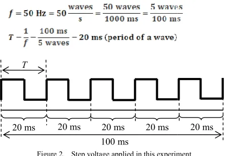
The voltage was applied to the spherical elec specimen, while the lower was connected to the system. The output of Function Generator was voltage, while HV Amplifier was square high vo measurement system, the discharge current specimen was integrated by means of the CR circ digitised using the peak detecting function of oscilloscope. The SDTL at a 7 kV step voltage w by applying periodical square HV pulses with 1 pulse width. The interval of pulse application wa was corresponded to 50 Hz, as shown in Figure 2.
Figure 2. Step voltage applied in this experime
The measurement is done by applying 64 pulses pulses and 64 negative pulses). A wave is consis i.e. one positive and one negative. In addition, resistivity is also measured using concentric geometry as shown in Figure 3 [4]. Where is o the center concentric electrode, is inner radius concentric ring electrode. Surface resistivity is re surface resistance by a constant that depends on the electrodes only:
. ……….. (1
where is frequency called a geometry coefficie surface resistivity is measured directly by the resi by utilizing various configurations of electro provides a constant voltage and measures t flowing between electrodes. The value of resistiv the value of resistance multiplied by the geometr Usually electrodes are especially constructed calculations of surface resistivity and the geomet
I would like to thank to Honda Denshi Corporation, Japan technical assistance in which the author could use Plasma Keyence ST 7010.
20 ms 20 ms 20 ms 20 ms 100 ms
by plasma. Before cleaned by ethanol. sma using a plasma
time was 3, 6, 11, is outer radius of r radius of the outer resistivity is equal to ometry coefficient. tructed to simply eometry coefficient
is equal to a simple integer. Most of i this simplified approach [5 7]. All expe at ambient condition.
Figure 3. Surface resistance measurement con electrodes
The wide application to determine t the chemical and physical changes lifetime of the insulator can only be understanding of the dependence of th all parameters affecting it [8].
III. RESULTS AND D
In order to explain the phenomen level of the exposure time soon after e investigated. According to the previous magnitude decreases with the increase however, the number of PD pulse incre the roughened surface, PD tends to plasma. This result is in agreement wit and Kosaki, M. [9]. The surface po smooth PMMA specimen has only one hand, the roughened one has a couple show that in the case of roughened surfa occurred at more than one place. It sug occurs if the dielectric materials w intensification of the local field. It is a roughness intensifies the local electric supply of the initial electrons. The peri PD inception voltage and the occurrenc lag. The SDTL is obtained at first exp result generates the cumulative pro Afterward, it is often converted into L probability ( ). In this plot, log is ma the time lag is the horizontal axis. Actua special meaning except that the parame shown more clearly than if we used the plot. l experiments were performed
nt configuration for concentric ring
mine the surface property and nges that occur during the increases with it, because, in nds to occur at many places face potential distribution of nly one peak. On the other ouple of peaks. These results ned surface specimens, the PD It suggests that the PD easily als were roughened due to It is assumed that the surface lectric field and increases the e period between the applied currence of PD is called time rst experimentation [3] whose e probability of time lag. d into Laue plot, i.e., residual
is made the vertical axis, and . Actually, this change has no parameter of time lag could be ed the cumulative probability
PMMA
Z2
According to that paper [3], the SDTL at 40 % residual probability 60 minutes after exposure by plasma tends to take longer time than that of 20 minutes. The time lag becomes longer probability related to the recovery time of material properties. Collections of ions and electrons remove gradually from the void surface. The ions and electrons are accompanying the exposure should be disappear gradually. It means that, following the time the effect of plasma exposure should be disappear. When the plasma effect was disappearing, it would make possible the discharge occur with longer time lag. This clarified that, for short exposure time the plasma treatment changes the surface properties of material only, not the bulk properties.
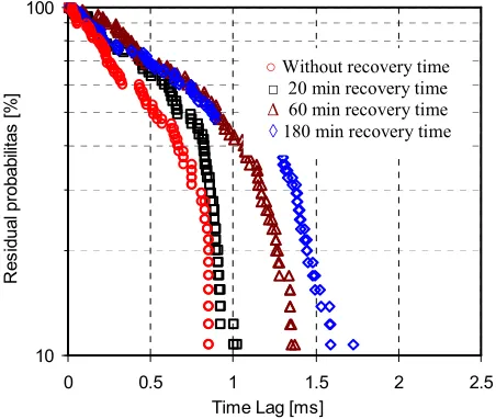
However, these results just only clarified that for typical short exposure time of 3 s, plasma treatment changes the surface properties of material only, not damage in deep of bulk specimen. It might be of somewhat speculated, since there was not enough data for 3 s exposure time. That is why in the present paper a new data has been added, as shown in Figure 4 to give more information about recovery times.
Figures 4 shows the typical Laue plots of SDTL for 3 s of exposure time. In this investigation, the recovery times of 20, 60, and 180 minutes were compared. As shown in Figure 4, the 3 s exposed specimen seems to have longer time lags as the increase of recovery times. It is considered that the specimens that already exposed by plasma radiation for 3 s, seems to be recover its insulating property after given recovery times of 20, 60, and 180 minutes compared to that of without recovery time. This result is in agreement with the previous results [3].
Figure 4. Laue plots of a 3 s plasma exposed specimen after 0, 20, 60, and 180 minutes of recovery times
Another result shows that PD easily occurs with a higher number of pulses when the surface of the specimen was degraded by plasma. This phenomenon may be due to surface change by plasma exposure, including an increase of surface roughness in combination with an increase of surface conductivity, as shown in Figure 5.
Figure 5. Surface conductivity of smooth and rough surfaces
A rough surface brought by plasma exposure would emphasize the electrical field so that the discharge with longer exposure time would more easily take place. Decrease in SDTL would make possible the PD occurring with a large number of small discharges. To ensure this effect, topographical images and profiles of surface roughness can be traced along the centre line of the eroded specimen by a laser microscope (Keyence VK 8510) to give the erosion profile shown in Figure 6 [10]. To give more detail information, one more image has been added in the Figure. It is recognized that the erosion increases as ageing time increases from 3 s to 21 s. The roughness of 3, 6, and 21 s of exposure time were 1.5, 6.3, and 8 m, respectively. In addition, many bumps were seen on the material surface. There is data scatter in the short range of position at the edges of micrographs. This is considered to be caused by original surface roughness of the specimens. This scatter had been extremely small compared to the erosion due to plasma exposure, thus it was assumed neglected.
IV. CONCLUSIONS
The SDTL due to deteriorations of high humidity of void space and dielectric surface in which void is bounded has been carried out using the CM II electrode system. The main results are summarised as follows.
(1) In both polarities, the time lag becomes shorter as the RH increases from 33 % to 98 %.
(2) The characteristic SDTL of positive polarity was shorter than that of negative polarity. This means that the SDTL with positive polarity was more sensitive to the applied voltage than with negative.
(#!"(' (#!"($
)3 3$ 43 ($$
,
*
5(
6
7
8 597
Smooth sample
Rough sample
10 100
0 0.5 1 1.5 2 2.5
Time Lag [ms]
R
e
s
id
u
a
l p
ro
b
a
b
ili
ta
s
[
%
]
○ Without recovery time
□ 20 min recovery time
M 60 min recovery time
◊ 180 min recovery time
Figure 6. Topographical images and profile of surface roughness of the specimens after being exposed by plasma for 3, 6, and 21 s, respectively.
(3) The SDTL also becomes shorter with increasing plasma irradiation time. It seems the initial electrons are more
easily supplied from a metallic electrode. A rough surface brought about by plasma irradiation would emphasize the electrical field so that the discharge (with a longer irradiation time) would more easily take place. Decrease in SDTL would make possible the PD occurring with large number of small discharges.
(4) In case of SDTL for 3 s exposures, the longer recovery time is given, the higher the specimen to recover its insulating property.
ACKNOWLEDGMENT
I am greatly indebted to Prof. Masayuki Nagao and Prof. Naohiro Hozumi, from Toyohashi University of Technology, Japan, for their suggestions and great supports.
REFERENCES
[1] Naidu, M. S. and Kamaraju, V. (1996). ! . New York: McGraw Hill.
[2] Diesendorf, W. (1974). " # !#$
% & . London: Butterworth.
[3] Zainuddin Nawawi, Husein Ahmad, Rudi Kurnianto, Naohiro Hozumi and Masayuki Nagao (2011). Statistical Discharge Time Lag in Insulation Gap Metal System Attributed to Dielectric Surface Conditioning and Relative Humidity Impact. ' $ % (
, April 2011.
[4] William A. Maryniak, Toshio Uehara, and Maciej A. Noras. “Surface Resistivity and Surface Resistance Measurements Using a Concentric Ring Probe Technique”, Trek Application Note, Number 1005, TREK INC., Medina, New York, 2003.
[5] ASTM Standard D 257 99. Standard test method for D C resistance or conductance of insulating materials, 1999.
[6] ESD STM 11.11 2001 Standard. Surface resistance measurement of static dissipative planar materials, 2001.
[7] IEC 61340 5 1 Standard. Electrostatics – part 5 1: Protection of electronic devices from electrostatic phenomena – general requirements, 1998.
[8] Hackam, R. Outdoor High Voltage Polymeric Insulators. Proceedings of International Symposium on Electrical Insulating Materials, in conjunction with Asian International Conference on Dielectrics and Electrical Insulation and the 30th
Symposium on Electrical Insulating Materials. Sept. 27 30, 1998. Toyohashi, Japan. 1–16.
[9] Ishida T., Nagao M. and Kosaki, M. Effect of Surface Roughness on Potential Distribution of Dielectric Materials after partial Discharge Exposure. &
) *+. September 27 30, 1998. Toyohashi, Japan. 669–672. [10] Z. Nawawi, H. Ahmad, R. Kurnianto, N. Hozumi and M. Nagao,
“Statistical Discharge Time lag in Insulation gap Metal System Attributrd to Dielectric Surface Conditioning and Relative Humidity Impact,” International Review of Electrical Engineering, Vol. 6 No. 1 Part B, pp. 445 451.
[11] Hozumi N., Michiue H., Nagae H., Muramoto, Y. and Nagao, M. Time lag Measurement of Void Discharges for the Clarification of the Factor for Partial Discharges pattern. ' " (
, ! )" , +. October 15 18, 2000. Victoria, Canada. 717 720.
Roughness [ m]
Section analysis
50 m
Exposure 3 s
Position [ m]
0 0.5 1
1.5
0 3 6 9 12 15 18 21 24 27 30
Exposure 3 s
Exposure 21 s
0 5 10
0 30 60 90 120 150 180 210 240 270 300
Section analysis
25 m
Position [ m]