Observation of Tunneling Effects in Lateral Nanowire pn Junctions
Sri Purwiyanti
1,2*, Arief Udhiarto
1,2, Daniel Moraru
1, Takeshi Mizuno
1, Djoko Hartanto
2, and
Michiharu Tabe
11. Research Institute of Electronics, Shizuoka University, Hamamatsu, Shizuoka 432-8011, Japan 2. Department of Electrical Engineering, Faculty of Engineering, Universitas Indonesia, Depok 16424, Indonesia
*e-mail: [email protected]
Abstract
As electronic device dimensions are continuously reduced, applied bias conditions significantly change and the transport mechanisms must be reconsidered. Tunneling devices are promising for scaled-down electronics because of expected high-speed operation and relatively low bias. In this work, we investigated the tunneling features in silicon-on-insulator lateral nanowire pn junction and pin junction devices. By controlling the substrate voltage, tunneling features can be observed in the electrical characteristics. We found that the minimum substrate voltage required for tunneling to occur in pn junctions is higher as compared with pin junctions. The main cause of these effects relies in the difference between the doping profiles, since the pn junctions contain a co-doped region, while the pin junctions contain an i-layer.
Abstrak
Pengamatan Efek Penyaluran dalam Persimpangan pn Pengantar Ukuran Nano Lateral. Sebagaimana dimensi-dimensi peralatan elektronik secara terus-menerus berkurang ukurannya, kondisi-kondisi bias yang diaplikasikan secara signifikan berubah dan mekanisme pengangkutan harus dipertimbangkan kembali. Peralatan penyaluran menjanjikan alat elektronik yang berukuran lebih kecil dan ringan karena diharapkannya pengoperasian dengan kecepatan tinggi dan bias yang secara relatif rendah. Dalam penelitian ini, kami menyelidiki fitur-fitur penyaluran dalam persimpangan pn pengantar ukuran nano lateral silikon pada insulator dan alat-alat persimpangan berukuran jarum. Dengan mengendalikan tegangan substrat, fitur-fitur penyaluran dapat diamati dalam karakteristik-karakteristik listrik. Kami menemukan bahwa tegangan substrat minimum yang diperlukan untuk penyaluran untuk terjadi dalam persimpangan pn lebih tinggi dibandingkan dengan persimpangan berukuran jarum. Penyebab utama efek-efek ini mengandalkan pada perbedaan-perbedaan antara profil-profil dengan doping, karena persimpangan pn berisi daerah yang dico-doped, sementara persimpangan seukuran jarum berisi lapisan i.
Keywords:nanowire, pn junction, silicon, tunneling
1. Introduction
Recent modern lithography capabilities allow the fabrication of semiconductor devices in nanometer scale. The advantages of nanoscale devices consist of high density, high operation speed and low applied voltage. Reduction in device dimensions, however, brings about several difficulties in conventional device operation, in particular related to the applied bias conditions [1]. In most semiconductor devices, the basic transport mechanism is thermal excitation of carriers over a potential barrier, but it is difficult to appropriately reduce the operating voltage while maintaining a good on/off current ratio. In order to reduce the operating voltage and take advantage of the quantum phenomena arising in nanostructures, the transport mechanism must
be drastically changed. In that sense, quantum tunneling is a promising candidate for improving the operation conditions. The first functional device operated based on the tunneling mechanism was the well-known Esaki diode, which is effectively a heavily-doped pn junction [2]. More recently, tunneling field-effect transistors (TFETs) [3,4] have been investigated, with their operation relying on band-to-band tunneling controlled by a gate voltage.
[6-8]. Tunneling in lateral pn junctions has been reported by Aydin et al. [9], but not in nanowire structures. Here, we focus on identifying tunneling characteristics in lateral pn junctions with nanowire channels.
In this work, we investigate in particular the behavior of the current versus applied bias characteristics with substrate voltage as a control parameter. We compara-tively study tunneling effects in lateral nanowire devices designed both as pn junctions and pin junctions.
2. Methods
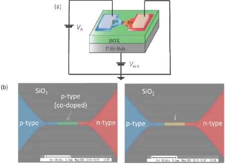
Device specification and measurement setup. We fabricated nanowire silicon-on-insulator (SOI) pn junctions, with structure schematically shown in Figure 1(a). Nanowires were patterned on the SOI layer by an electron beam (EB) lithography technique. Then, a selective doping technique was used to create the n-type (phosphorus-doped) and p-type (boron-doped) regions. The nanowire length and thickness are designed as 1000 nm and 10 nm, respectively, while the nanowire width is set as a parameter, varying from 75 nm to 275 nm in this study. Aluminum contact pads were formed as electrodes.
Both pn and pin junctions were fabricated on the same sample. pn junctions contain a co-doped region, which was intentionally doped both with phosphorus (P) and boron (B) dopants. In the pin devices, an area in the middle part of the nanowire was kept un-doped, as an i -layer. Schematic views of the co-doped and pin devices are shown in Figure 1(b). B concentration was set higher than P concentration and, as a result, the co-doped region is effectively p-type, with a net concentration NA ≈ 0.5×1018 cm-3. For both devices,
final P and B concentrations, derived from secondary ion mass spectrometry (SIMS), are estimated to be ND ≈
1×1018 cm-3 and N
A ≈ 1.5×1018 cm-3, respectively. The
Figure 1. (a) Device Structure and Bias Configuration for Electrical Characterization. (b) Co-doped (left) and pin (Right) Devices, based on SEM Images. Co-doped and Intrinsic Region are Located within the Thin and Narrow Nanowire
p-Si substrate was doped with boron (NA ≈ 1.5×10¹⁸
cm-3) and was used as a gate throughout the
experiments. The thickness of the buried oxide layer between the nanowire and the substrate is 150 nm. The nanowire is covered with a 10-nm-thick SiO2 layer,
grown by thermal oxidation.
Devices were measured in a vacuum chamber of an electrical measurement system. Electrical characteristics were measured with the p-type region and substrate connected to variable voltage sources, while the n-type region was kept grounded.
3. Results and Discussion
In this section, we analyze the measured current (I) - substrate voltage (Vsub)-applied bias (VA) characteristics,
focusing on the tunneling features.
I-Vsub characteristics. We measured I-Vsub
characteris-tics at room temperature for various VA values, while
Vsub was gradually increased from -10 V to 15 V. The
typical I-Vsub characteristics, with the vertical axis
indicating the absolute value of the current I, for a pin device are shown in Figure 2.
For forward bias (VA > 0V), it can be seen that current
is enhanced in the range Vsub = -10 ~ 3 V. When Vsub is
at positive values, current is reduced and, finally, for Vsub above 12 V, current exhibits an abrupt increase. For
reverse bias (VA = -0.5 and -1 V), current is very small
for negative Vsub. For Vsub > 6 V, however, current starts
to slowly rise and, again, for VSUB > 12 V, current
abruptly increases. This common behavior observed for large Vsub values, i.e., above 12 V, for both forward and
reverse biases, can be related to the onset of tunneling transport in our devices. The basic mechanism will be explained in the following.
We can analyze this behavior starting from the energy band diagrams of the devices, as shown in Figure 3. In equilibrium and for Vsub = 0 V, the Fermi levels in p
-type – i-layer – n-type are aligned. When positive bias is applied to the p-type region, as in the forward-bias case illustrated in Figure 3(a), the Fermi level of the p-type will be shifted downwards and current starts to flow. If Vsub is increased from 0 V to more positive values, with
VA kept constant in this forward-bias condition, the
Figure 2. Typical I-Vsub Characteristics for a pin Device in
Forward and Reverse Bias (as Indicated on the Curves) at Room Temperature. Vertical Axis Indicates the Absolute Value of Current I
Figure 3. Band Diagrams of pin Junction and I-Vsub
Characteristics for: (a) Forward Bias and (b) Reverse Bias. VA is Constant, While Vsub
Gradually Increases from 0 V to Positive Voltages
more positive voltages, additional electrons injected into After reaching the maximum current, by further increasing Vsub, the concentration of holes in the i-layer
is drastically decreased, leading to a significant reduction in the recombination current, observed in Figure 2 in the range Vsub = ~3 ~12 V. When Vsub is
increased to much larger values, the conduction band edge of the i-region approaches that of the n-type region. The depletion region moves from the n-type edge to the p-type edge and, consequently, the location of the recombination processes shifts towards the p-type region. Eventually, the i-layer conduction band edge becomes slightly lower than the n-type band edge and, as a result, electrons can be accumulated in the conduction band of the i-region. From there, electrons can recombine easily with holes in the valence band of
the p-type region, assisted by tunneling via states in the band gap. As a result, current is drastically increased, as seen in Figure 2 for Vsub >12 V. This mechanism is
effectively a recombination process enhanced by tunneling effects.
Under reverse bias conditions [Figure 3(b)], a small electron current can flow from the p-type region to the n-type region. When Vsub is increased from -10 V to the
i-layer will quickly recombine with holes, giving rise to a small current which is practically independent of Vsub,
in Vsub range of -10 V ~ 6V (as shown in Figure 2).
When Vsub is further increased, the concentration of
holes available for recombination in the i-layer is reduced and, therefore, additional electrons are flowing as drift current. As a consequence, reverse current is enhanced. By increasing Vsub even more, the conduction
band edge of the i-region potential will be shifted below the band edge of the n-type region and electrons can tunnel from the valence band of the p-type region to the conduction band of the i-region. This band-to-band tunneling leads to the abrupt increase of the reverse current for Vsub > 12 V. This mechanism is basically
similar to that of tunneling FETs.
I-VA characteristics. We also measured the current
versus applied bias (I - VA) characteristic at room
temperature for various Vsub, while VA was gradually
increased from -5 to 2 V. Typical I-Vsub characteristics
for pn device are shown in Figure 4. It can be seen that in the forward bias (VA > 0 V), the dependence of current
on Vsub has a particular behavior. First, by increasing
Vsub from 0 to 6 V, current level is gradually reduced.
However, for Vsub > 6 V, current level is increased and
the features of the I-VA change significantly. For reverse
bias (VA < 0 V), the current exhibits a more systematic
behavior, as current level gradually increases with Vsub.
The origin of this behavior is related to the potential changes occurring in particular in the depletion region, as illustrated in Figure 5.
Figure 4. Typical I-VA Characteristics of pn Device for
Various Vsub Values (Indicated on the Curves) at
Figure 5. Changes of the Depletion Region Location Due to Gradually Increasing Vsub, Illustrated from (a) to (c), for
Constant Forward Bias
For low forward bias and Vsub = 0 V, the depletion
region location is at the n-type edge and electrons flow from the n-type region to the p-type region as diffusion current (Figure 5(a)). It should be noted that, in our devices, the co-doped region is actually p-type with lower concentration, as we explained above.
By increasing Vsub, the number of ionized B acceptors in
the co-doped region is enhanced. In order to reach the charge neutrality condition, the depletion region becomes wider, which leads to a decrease of the recombination current by increasing Vsub. For
intermediate Vsub (most likely, for 6 V in our
experimental results), the depletion region location is in the entire co-doped region (Figure 5(b)). In this condition, a minimum is observed in the measured current. For Vsub larger than this value, the depletion
region width becomes smaller and gradually moves to the p-type region. The location of the key recombination events moves as well from the co-doped region to the p -type region. Therefore, current is observed to enhance by increasing Vsub (Figure 5(c)).
When Vsub is further increased, the conduction band
edge of the co-doped region falls below the conduction band edge of n-type region. In this condition, the Fermi level of co-doped region is close to the Fermi level of the p-type region. As a result, electrons can tunnel from the valence band of the p-type region to the conduction band of the n-type region. Thus, tunneling mechanism plays an essential role in the electrical characteristics of nanowire lateral pn and pin junctions.
The I-VA-VSUB characteristics. In order to visualize a
more complete picture of the device behavior, we have plotted I-Vsub-VA graphs for pin and pn junctions, as
shown in Figure 6. The nanowire dimensions are comparable for both types of devices, i.e., 1000 nm in length and 275 nm in width.
In the pn junction characteristics (Figure 6(a)), for reverse bias (for instance, for VA = -1.5 V), current
slightly increases when Vsub is increased gradually from
-5 to 5 V. Current, however, increases more drastically for Vsub above 5 V. It shows that a minimum substrate
voltage required for tunneling effects to occur is 5 V. In forward bias (for instance, for VA = 1.5 V), when Vsub is
gradually increased from -5 to 10 V, current first increases, then decreases and, finally, increases again at most positive Vsub values. This indicates that the
condition of tunneling in forward bias is more complicated compared to that in the reverse bias. This situation may be related to the changes occurring in the depletion region location, as described above, in Figure 5. higher Vsub for tunneling compared to the pin junction.
doping concentrations between i-region of pin junction and co-doped region of pn junction. The higher concentration of B acceptor dopants in the co-doped region leads to higher Vsub required for pn junctions to
adjust the energy band conditions. The effects of the effective doping concentration in the region between the n- and p-type pads require, however, further investigation before being fully clarified.
4. Conclusions
We observed tunneling effects in lateral nanowires, designed as pin and pn junctions. We found that tunneling events occur in both reverse and forward bias, under appropriate biasing conditions. The minimum substrate voltage required for tunneling depends on the doping concentration in the junction. Further measurements will reveal the effects of different doping concentrations and doping profile on the tunneling characteristics, providing useful information for understanding the behavior of nanoscale pn junctions operated in tunneling mode.
References
[1] The Semiconductor Industry Association, The International Technology Roadmap for Semicon-ductors (ITRS), 2011 Edition, http://www.itrs.net/, 2011.
[2] L. Esaki, Phys. Rev. 109 (1958) 603.
[3] A.M. Ionescu, H. Riel, Nature 479 (2011) 329. [4] D. Leonelli, A. Vandooreen, R. Rooyackers, S.D.
Gendt, M.M. Heyns, G. Groeseneken, Solid-State Electron. 65-66 (2011) 28.
[5] S.M. Sze, Physics of Semiconductor Devices, 2nd ed., John Wiley & Sons, New York, 1981, p.880. [6] S. Sedlmeier, J. Schulze, T. Sulima, C. Fink, C.
Tolksdorf, A. Bayerstadler, I. Eisele, P.F. Wang, K. Hildensenbeck, W. Hansch, Mater. Sci. Eng. B 89 (2002) 116.
[7] H. Schmid, C. Bessire, M.T. Bjork, A. Schenk, H. Riel, Nano Lett. 12 (2012) 699.
[8] C.D. Bessire, M.T. Bjork, H. Schmid, A. Schenk, K.B. Reuter, H. Riel, Nano Lett. 11 (2011) 4195. [9] C. Aydin, A. Zaslavsky, S. Luryi, S. Cristoloveanu,