Integrated Circuits and Systems
Series Editor
Anantha P. Chandrakasan
For further volumes:
Editor
Applications of Organic
and Printed Electronics
A Technology-Enabled Revolution
Eugenio Cantatore
Department of Electrical Engineering Eindhoven University of Technology Eindhoven
Netherlands
ISSN 1558-9412
ISBN 978-1-4614-3159-6 ISBN 978-1-4614-3160-2 (eBook) DOI 10.1007/978-1-4614-3160-2
Springer Boston Heidelberg New York Dordrecht London
Library of Congress Control Number: 2012944381
Springer Science+Business Media New York 2013
This work is subject to copyright. All rights are reserved by the Publisher, whether the whole or part of the material is concerned, specifically the rights of translation, reprinting, reuse of illustrations, recitation, broadcasting, reproduction on microfilms or in any other physical way, and transmission or information storage and retrieval, electronic adaptation, computer software, or by similar or dissimilar methodology now known or hereafter developed. Exempted from this legal reservation are brief excerpts in connection with reviews or scholarly analysis or material supplied specifically for the purpose of being entered and executed on a computer system, for exclusive use by the purchaser of the work. Duplication of this publication or parts thereof is permitted only under the provisions of the Copyright Law of the Publisher’s location, in its current version, and permission for use must always be obtained from Springer. Permissions for use may be obtained through RightsLink at the Copyright Clearance Center. Violations are liable to prosecution under the respective Copyright Law.
The use of general descriptive names, registered names, trademarks, service marks, etc. in this publication does not imply, even in the absence of a specific statement, that such names are exempt from the relevant protective laws and regulations and therefore free for general use.
While the advice and information in this book are believed to be true and accurate at the date of publication, neither the authors nor the editors nor the publisher can accept any legal responsibility for any errors or omissions that may be made. The publisher makes no warranty, express or implied, with respect to the material contained herein.
Printed on acid-free paper
The Disruptive Potential of Low-Cost,
Low-Temperature Technologies for Electronics
Electronics, and more specifically integrated circuits (IC), have dramatically changed our lives and the way we interact with the world. Following the so-called Moore’s law [1], IC complexity is growing exponentially since 40 years, and this trend is predicted to continue at least for the coming 15 years [2]. The abundance of electronic functions at affordable cost has enabled a wealth of applications where the main IC strengths, namely computational speed and memory capacity, are well exploited: PCs, portable devices, game consoles, smart phones and alike. The commercial success of integrated electronics is based on a symbiotic development of technology and applications, where technical progress and economic growth nurture each other. This process requires lots of time and effort: first IC patents where filed in 1949 [3], but it is only in 1971 that the first commercially available microprocessor (Intel 4004), one of the most far-reaching application of ICs, gained the market; and PCs became popular only in the second half of the eighties.
The main strength of integrated electronics is in the low-cost-per-function enabled by an ever growing miniaturization: mono-crystalline silicon real estate is very expensive, but the number of transistors that can be integrated per area grows according to Moore’s law, bringing down the cost to realize a given function.
Since the second half of the seventies, a completely different electronic para-digm, the so-called large-area electronics, has been developing. In this field the major aim is to decrease the cost per area (instead of the cost per function), enabling large surfaces covered with electronic devices. The main application of this kind of technology, typically based on amorphous or polycrystalline silicon transistors, is in active-matrix addressing of flat displays. The success of this technology has become evident in the last decade, when flat-panel LCD displays have swiftly replaced traditional cathode ray tubes in television sets.
Amorphous and polycrystalline silicon technology typically require high-tem-perature vacuum-based processing, with the consequence that glass substrates are
used and that the technology throughput is limited. In the nineties a new technology approach has been proposed, based on materials that enable low-temperature pro-cessing and the use of very high throughput patterning technologies, borrowed from the graphic printing field: organic and printed electronics were born.
The word ‘‘organic electronics’’, which I personally started using in 2000 [4] together with many colleagues, designates electronics manufactured using func-tional carbon-based materials, typically semiconductors, like pentacene, P3HT, PCBM, PTAA and many others. There are several reasons for this choice:
• Organic materials can form functional films when processed from solutions, paving the way to manufacturing processes with a reduced number of vacuum steps (which are typically expensive and cumbersome to scale to large areas), and thus enabling potentially very low-cost large-area electronics;
• Organic materials are processed at low temperature (typically below 200 C), enabling the use of inexpensive and flexible plastic foils as substrates and paving the way to flexible electronics;
• Organic chemistry is intrinsically very rich, enabling the exploration of a lim-itless library of materials having very diverse electrical, optical, rheological and chemical properties;
• Together with the chemical variety, a large spectrum of physically different devices based on organic materials is possible and has been developed in the years, the most well-known being organic light emitting diodes (OLEDs) [5], organic thin-film transistors (OTFTs) [6, 7], organic photovoltaics (OPVs) [8], organic sensors [9], organic memories [10, 11], and organic MEMs [12]1.
Together with these strengths, functional organic materials and organic elec-tronics present a number of drawbacks:
• Organic semiconductors have a relatively poor mobility, with peak values for single-crystal materials in the range of 10 cm2/Vs [13], and typical values in
solution-processed films of about 1 cm2/Vs at the state of the art. Under this
point of view, other materials suitable for low-temperature and large-area pro-cessing, like metal-oxide semiconductors and carbon nanotubes, may offer an advantage compared to organic semiconductors.
• Organic semiconductors (especially n-type) are sensitive to oxygen, moisture and other environmental aggressors, so that for long time organic electronic devices have had poor shelf and operational lifetime. Organic materials are also sensitive to bias stress, which tends to affect operational lifetime. Recent improvements in the materials, their formulation and encapsulation, however, show that instabilities should not be a show-stopper for commercialization (see for instanceSect. 2.3inChap. 2andSect. 4.4inChap. 4);
• Organic semiconductors are difficult to dope in situ with highly controlled dopant concentrations as a process equivalent of the ion implantation doping used in silicon has still not been developed for organic materials. This makes difficult to manage key parameters like transistor threshold voltages and injec-tion barriers at the contacts.
Many more details on the state of the art and roadmaps of organic electronics are given inChap. 1and in the other chapters of this book.
The capability to deposit organic materials from solution makes possible to pattern functional materials using methods adapted from graphic printing, like inkjet, gravure, slot coating and many others. This leads to the concept of ‘‘printed electronics’’. The main strength of this approach is the high throughput that characterizes printing production processes, which means that printing has the potential to make possible very inexpensive large-area electronics, and thus to enable applications of electronics unthinkable till now. Moreover, printing is an additive process, thus only the functional materials that are needed are effectively used, contrary to the traditional lithography-based subtractive approach. This has the potential to decrease material usage and thus further bring down the costs. Detailed information on printing electronics is available especially inChaps. 1,2 and6 of this book.
The strengths of printing are paired with the challenges that this technology faces: it is namely difficult and expensive to develop a new electronic technology using an approach that in a few minutes can generate rolls covered with hundreds of meters of electronics to be characterized and optimized. Uniformity, perfor-mance and yield are daunting tasks to be solved for future printed electronics applications.
The potential low cost, the compatibility with large flexible substrates and the wealth of devices that characterize organic and printed electronics will make possible applications that go far beyond the well-known displays made with conventional large-area silicon electronics. Organic and printed electronics can enable a true revolution in the applications of electronics: this is the view that brought me, together with a large number of colleagues, to write this book. The volume offers to the reader an extensive overview of the different devices enabled by organic electronics, and reviews a large variety of applications that are developing and can be foreseen for the future.
Chapter 1, written by Tampere University, the Organic Electronic Association (OA-E) and PolyIC, offers a complete Roadmap for Organic and Printed Elec-tronicsspanning till the end of this decade. It is an ideal starting point to under-stand the complex application scenarios and the likely developments in this rapidly growing technology domain.
the structures in the plane of the device, and are thus an ideal candidate to exploit the high throughput of printing processes. This chapter is an excellent reading for the person willing to understand more about printing electronics. A roadmap for organic solar cells concludes this contribution.
In the third and fourth chapter light emitting diodes (OLED), the most advanced organic electronic devices available at the moment, are discussed. Chapter 3, written by Kyung Hee University and Samsung, gives a detailed overview of OLED Displays, a booming application that has reached the market since some years already, and is rapidly growing to become the standard emissive technology for flat displays. This section informs the reader about the different types of OLED pixels in commercial use and in development, and gives insight into the most relevant display and backplane issues.
Chapter 4, by Philips, gives a nice overview ofOLED for Lightingapplications. The section begins with an insightful description of the materials, physics, architecture and benchmarking of OLED lighting devices, to continue with an overview of fabrication methods, reliability and commercial applications.
Chapter 5by University of Tokyo gives an interesting vision for future organic electronics: it will complement silicon ICs to create new applications enabling unprecedented ways of interaction between electronics and people. In this vision are included a variety of different organic devices (TFTs, sensors and actuators) providing a stimulating view on how different types of organic electronics can be integrated to enable revolutionary applications.
The sixth and seventh chapter deal with organic TFTs. Chapter 6focuses on applications ofPrinted Organic TFTs. This section, written by PolyIC, describes the devices and technology needed to print transistors and circuits, the charac-teristics of printed TFTs, and what this revolutionary technology can mean in terms of applications (RFIDs and Smart Objects). Chapter 7 by IMEC, KUL, KHL, TNO and Polymer Vision focuses on the application of Organic TFTs to low-costRFIDs. This section explains how organic RFIDs are developing towards becoming fully-compliant to existing standards for RFIDs based on silicon IC technology. Compatibility with standards would mean that the same infrastructure can be shared between silicon and organic RFIDs, enabling a seamless transition between the two technologies and an easy market uptake. This does not mean, however, that silicon and organic should serve the same markets: the character-istics of printed electronics lend themselves naturally to the dream of enabling item-level identification of retail items, which is still out of reach for silicon RFIDs, due to the high costs and cumbersome integration of silicon ICs with the items to be identified.
This book can be read at different levels of insight by beginners as well as by experts in the field, and is specifically conceived to address a wide range of people with technical and scientific background. I am deeply grateful to all contributors: I hope you will appreciate their effort and I wish you a pleasant and fruitful reading.
Eindhoven, The Netherlands, January 2012 Eugenio Cantatore
References
1. Moore GE (2003) No exponential is forever: but ‘‘forever’’ can be delayed! In: ISSCC 2003 digest of technical papers, pp 20–23
2. ITRS Roadmap (2011) Available at http://www.itrs.net/Links/2011ITRS/ Home2011.htm
3. Jacobi W (1949) Halbleiterverstärker, Patent DE833366, 15 April 1949 4. Cantatore E (2001) State of the art electronic devices based on organic materials.
In: Proceedings of the 31st European solid-state device research conference (ESSDERC), pp 25–34
5. Tang CW, VanSlyke SA (1987) Organic electroluminescent diodes. Appl Phys Lett 51:913
6. Koezuka H, Tsumura A, Ando T (1987) Field-effect transistor with poly-thiophene thin film. Synth Met 18:699–704
7. Brown AR, Pomp A, Hart CM, de Leeuw DM (1995) Logic gates made from polymer transistors and their use in ring oscillators. Science 270(5238): 972–974
8. Sariciftci NS, Smilowitz L, Heeger AJ, Wudl F (1992) Photoinduced electron-transfer from a conducting polymer to buckminsterfullerene. Science 258(5087):1474–1476
9. Torsi L, Dodabalapur A, Sabbatini L, Zambonin PG (2000) Multi-parameter gas sensors based on organic thin-film-transistors. Sens Actuators B 67:312 10. Reed MA, Chen J, Rawlett AM, Price DW, Tour JM (2001) Molecular
random access memory cell. App Phys Lett 78(23):3735–3737
11. Ouyang JY, Chu CW, Szmanda CR, Ma LP, Yang Y (2004) Programmable polymer thin film and non-volatile memory device. Nat Mater 3(12):918–922 12. Sekitani T, Takamiya M, Noguchi Y, Nakano S, Kato Y, Hizu K, Kawaguchi H, Sakurai T, Someya T (2006) A large-area flexible wireless power transmission sheet using printed plastic MEMS switches and organic field-effect transistors. In: IEEE int. electron devices meeting (IEDM), pp 287–290
Contents
1 OE-A Roadmap for Organic and Printed Electronics . . . 1 Donald Lupo, Wolfgang Clemens, Sven Breitung and Klaus Hecker
2 Solution-Processed Organic Photovoltaics. . . 27 Claudia N. Hoth, Pavel Schilinsky, Stelios A. Choulis,
Srinivasan Balasubramanian and Christoph J. Brabec
3 High-Performance Organic Light-Emitting Diode Displays . . . 57 Jang Hyuk Kwon, Ramchandra Pode, Hye Dong Kim
and Ho Kyoon Chung
4 High Efficiency OLEDs for Lighting Applications. . . 83 Coen Verschuren, Volker van Elsbergen and Reinder Coehoorn
5 Large Area Electronics with Organic Transistors . . . 101 Makoto Takamiya, Tsuyoshi Sekitani, Koichi Ishida,
Takao Someya and Takayasu Sakurai
6 Printed RFID and Smart Objects for New High
Volume Applications . . . 115 Wolfgang Clemens, Jürgen Krumm and Robert Blache
7 Organic RFID Tags. . . 133 Kris Myny, Soeren Steudel, Peter Vicca, Steve Smout,
Monique J. Beenhakkers, Nick A. J. M. van Aerle, François Furthner, Bas van der Putten, Ashutosh K. Tripathi, Gerwin H. Gelinck, Jan Genoe, Wim Dehaene and Paul Heremans
8 Printed Organic Chemical Sensors and Sensor Systems. . . 157 Vivek Subramanian, Josephine Chang and Frank Liao
Chapter 1
OE-A Roadmap for Organic
and Printed Electronics
Donald Lupo, Wolfgang Clemens, Sven Breitung and Klaus Hecker
Abstract The roadmap for organic and printed electronics is a key activity of the OE-A, the industrial organisation for the young organic, printed and large area electronics industry. Organic electronics is a platform technology that enables multiple applications, which vary widely in their specifications. Since the tech-nology is still in its early stage—and is in the transition from lab-scale and pro-totype activities to production—it is important to develop a common opinion about what kind of products, processes and materials will be available and when. This chapter is based on the third version of the OE-A Roadmap for organic and printed electronics, developed as a joint activity by key teams of experts in 9 applications and 3 technology areas, informed by further discussions with other OE-A members during association meetings. The resulting roadmap is a synthesis of these results representing common perspectives of the different OE-A forums. Through com-parison of expected product needs in the application areas with the expected technology development paths, potential roadblocks or ‘‘red brick walls’’ such as resolution, registration and complementary circuitry are identified.
D. Lupo (&)
Department of Electronics, Tampere University of Technology, PO Box 692, 33101 Tampere, Finland
e-mail: [email protected] W. Clemens
PolyIC GmbH and Co.KG, Tucherstrasse. 2, 90763 Fürth, Germany e-mail: [email protected]
S. BreitungK. Hecker
OE-A (Organic Electronics Association), c/o VDMA, Lyoner Street 18, 60538 Frankfurt am Main, Germany
e-mail: [email protected] K. Hecker
e-mail: [email protected]
E. Cantatore (ed.),Applications of Organic and Printed Electronics, Integrated Circuits and Systems, DOI: 10.1007/978-1-4614-3160-2_1, Springer Science+Business Media New York 2013
Keywords Organic electronics
Printed electronics Roadmap OE-A applica-tionsRed brick walls
Organic electronics association
1.1 Introduction
Organic and printed electronics is based on the combination of new materials and cost-effective, large area production processes that open up new fields of appli-cation. Thinness, light weight, flexibility and environmental sustainability are key advantages of organic electronics. Organic electronics also enables a wide range of electrical components that can be produced and directly integrated in low cost reel-to-reel processes.
Intelligent packaging, low cost RFID (radio-frequency identification) tran-sponders, rollable displays, flexible solar cells, disposable diagnostic devices or games, and printed batteries are just a few examples of promising fields of application for organic electronics based on new, large scale processable, elec-trically conductive and semi-conducting materials.
The following pages present a short overview of organic electronics applica-tions, technologies and devices, as well as a discussion of the different technology levels that can be used in manufacturing organic electronic products, based on the third edition of the roadmap developed by the OE-A. Since the second edition we have added further applications that we expect to play a key role in the com-mercialization of this emerging technology and taken account of the exciting technical progress made recently.
In the applications section which follows, the market entry on larger scales for the various applications is forecasted. The key application and technology parameters relating to these applications and the principle challenges (so-called red brick walls) to achieving these have been identified. In the subsequent tech-nology section we summarise the projected development of relevant technologies and take account of recent progress in new materials and improved processes.
A White Paper explaining the current edition of the roadmap in more detail can be downloaded [1].
Organic electronics
1.2 Applications
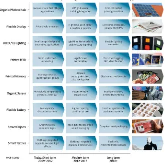
Organic and printed electronics is a platform technology that is based on organic conducting and semi-conducting as well as printable inorganic materials. It opens up new possibilities for applications and products. A number of key applications of organic and printed electronics have been chosen to demonstrate the needs from the application side, identify major challenges, cross check with the possibilities of the technology and to forecast a time frame for the market entry in large volumes. Below, we continue to look at applications discussed in the second edition of the roadmap. i.e. organicphotovoltaic cells (OPV), printedRFIDs, organicmemories, organicsensors, flexiblebatteriesandsmart objects. We also expand on the pre-vious application area of organic thin film transistor (OTFT) display backplanes to look atflexible displays, and look at two new application areas, electroluminescence (EL)and organic LED(OLED) based lightingandsmart textiles.
The growing list of applications reflects the complexity of the topic and the wide possible uses for organic electronics, and it is likely that the list will even grow in the future. The application fields and specifications cover a wide range, and although several parameters like accuracy of the patterning process or electrical conductivity of the materials are of central importance, the topic cannot be reduced to one single parameter at the time being, as is known from the famous Silicon Roadmap (Moore’s law). Regardless, we will watch the trends and find out whether it will be possible to find an analogue to Moore’s law for organic electronics.
The question whether there is one ‘‘killer application’’ for organic electronics cannot be answered at this moment. There are many different fields in which the advantages of organic electronics might result in the right product to become the killer application, but at this point, it is too early to define which one it is. Past experience with new technologies has shown that the predicted ‘‘killer applica-tions’’ are frequently not the ones that really open up the largest markets. Therefore, one has to continue the work on the roadmap, as is planned, follow the actual trends and take account of new developments as they occur.
memories, have already been demonstrated technically and have recently approached the market. Within 2–4 years, it is expected that mass markets will be reached and that all the above mentioned applications, and several more, will be available in large volumes.
1.2.1 Applications Roadmap
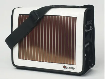
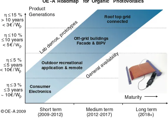
Dye sensitised solar cell (DSSC) basedorganic photovoltaicproducts have been produced commercially since 2007 [8]. First polymer OPV products have been shipped, with increasing commercial availability, e.g. as flexible solar cells (see Fig.1.1) for a battery charger for mobile phones. For the next few years OPV will primarily address consumer, outdoor recreational and initial off-grid markets, but as efficiency and lifetime improve the target is to move into building integrated PV (BIPV) and off-grid power generation mid-term and, in the long term, enter the on-grid power generation market. This will require significant technical progress in materials and processes to deliver high efficiency, highly stable products. In this book organic photovoltaics are further discussed inChap 2.
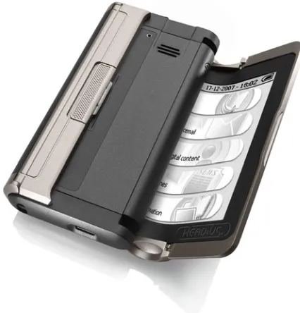
Flexible displays are starting to enter the market, with roll to roll produced segmented electrophoretic price labels already being used in stores and rollable e-reader devices with OTFT backplanes (Fig.1.2) and large area unbreakable OTFT based e-reader products test marketed 2011. Displays based on electro-phoretic or electrochromic media or on OLEDs are currently getting a particularly large amount of attention, but displays based on liquid crystals, electrowetting etc. are also possible. Further in the future, both reflective and emissive colour displays and large area products like rollable OLED TVs or electronic wallpaper are anticipated. However, the move to colour, high resolution and OLEDs will require significant improvements in backplane patterning tech-nology, display media and OTFT technology.
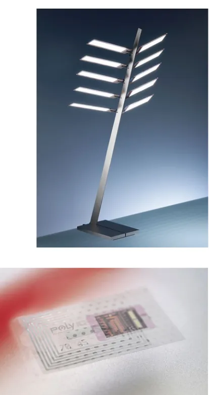
Electroluminescent (EL) and OLED Lightingis an application that is new to the third edition of the roadmap. While OLEDs have been penetrating the display market for some time now, only recently have significant improvements in effi-ciency, lifetime and large area devices made OLED an important potential source of novel large-area, energy efficient solid-state lighting. EL signage and backlighting is already commercial, first OLED designer lamps (Fig.1.3) are already available, and in the future OLED lighting will move from being a technology for design and decorative applications to technical lighting and general illumination; this will however, require both very high efficiency, colour purity and lifetime as well as development of processes, materials and architectures to cut production costs. Chap. 4of this book further addresses OLED lighting and its applications.
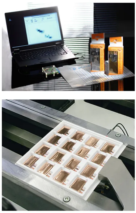
Printed RFID (radio frequency identification) based on organic electronics showed significant technical progress since the last edition of the roadmap, with announcements of advances such as roll to roll printed high frequency (HF) tags with 1–4 bits, as well as first organic CMOS-like circuits [9], 128 bit transponders [10], and ultrahigh frequency (UHF) rectifiers [11], all based on organic semi-conductors. In addition, there has been progress with alternative approaches such as chipless RFID concepts. Printed antennas are already common in conventional Si-based RFID products. A further approach for printed transponders is based on Si nanoparticles on stainless steel substrates. These approaches are not further taken into account in the current roadmap discussion, as this roadmap focuses on organic/printed chips on plastic substrates. The activities of printed RFID are targeting towards Electronic Product Code (EPCTM) compatible tags in the long
term (seeChap. 7), even though the general performance of printed RFID will be on a lower level compared to standard RFID tags for a long time. Simple printed
RFID tags (Fig.1.4) were piloted already in 2007 and should be in general commercial use within the next few years. The future is expected to bring a trend to larger memory, and to UHF as well as HF tags. The expected applications range from brand protection into ticketing, identification, automation and logistics, as the technology advances. Despite some delays in market introduction of simple RF circuits, the rapid technical progress in the recent past makes us optimistic that more advanced products will actually be available within the next years. Keys to this progress will be mature high volume and low cost production processes, fast circuits, smaller dimensions and CMOS-like circuit development, as well as appropriate standards for organic RFID products. RFIDs are the main subject of Chaps. 6and7of this book.
Fig. 1.3 OLED designer lamp.SourceOSRAM Opto semiconductors
Printed Memory devices have already been introduced to the market in the form of Read-only Memories (ROM) or Write Once Read Many (WORM) memories in ID or game cards. Recently reel to reel fabrication of printed rewritable non-volatile Random Access Memories (NV-RAM) was technically demonstrated [12], and first low-density polymer NV-RAM products are available on the market (Fig.1.5). Future generations of printed memory products will see a trend to higher bit density, faster reading and writing, on-board readout and a trend to more NV-RAM, though ROM and WORM will remain important. Key tech-nical issues to resolve in the future will include scaling of on-board readout electronics and memory cells.
Organic Sensordevices (Fig. 1.6) open up a variety of applications. The field has developed more rapidly than expected, with prototype temperature, chemical and pressure sensors already demonstrated. Temperature, pressure and photodiode sensors and sensor arrays will reach the market in the next few years. One trend will be from yes/no sensors to analog sensors able to give a quantitative readout. For example, potentiometric sensors for chemical analysis are already starting to become available in a yes/no configuration but analog versions will be available midterm. In the long term, combination of sensor devices into embedded systems including on-board (organic) circuitry and possibly on-board display-based read-out is expected to enable intelligent sensor systems. This will require significant advances not only in the sensors themselves but also in the associated on-board circuitry, which will require high reproducibility, reliability, yield, etc. Sensors are further discussed inChap. 8of this book, while integration with circuits to enable intelligent sensor systems is addressed inChaps 6and7
Thin and flexible batteries(Fig.1.7) are already commercially available for discontinuous use, but there is room for improvement in price, capacity and ease of integration into some systems. Over the next few years a trend to commercial availability of cost-effective low capacity batteries, then higher capacity batteries for continuous use and finally batteries that can be directly printed into electronic
systems or packages is expected. Key areas for development will be optimisation of cost-effective production and encapsulation of Li based thin batteries.
A big advantage of organic electronics is the combination and simple inte-gration of multiple electronics devices to create smart objects. As simple example, printed keypads, printed loudspeakers and smart cards incorporating thin film batteries and flexible displays (Fig.1.8) have been shown [13]. In the future the trend will be towards inclusion of more different functionalities as well as more complex functionalities, moving from simple input devices, animated logos or smart cards to objects with full displays, intelligent tickets and sensors, games, and smart packages. The variety of smart objects will be limited only by the number of organic electronic technologies available and the creativity of product developers. One of the key issues to look at will be taking care of mechanical and electrical compatibility and connection between the different functions.
Another new application in the current roadmap is smart textiles, in which functionalities such as communication, displays, sensors, or thermal management
Fig. 1.6 Large-area organic based pressure sensor array. SourcePlastic electronic
are integrated into fabric to enable wearable electronics (Fig.1.9). First examples of integration of LEDs, optical fibers or electroluminescent elements into apparel are already starting to hit the market [14,15]. Application areas range from sport, fashion, safety and health clothing to architecture, and over time the technology will become more complex, moving from simple sensors, keypads, light effects etc. in the short term to more complex systems incorporating functionalities like OPV, fuel cell and textile sensors in the future.
These application scenarios are summarized in theOE-A roadmap for organic electronics applications in Fig.1.10. For each of the nine selected applications we show products that are expected to reach the market in the short (2009–2012) and medium term (2012–2017). We also give a forecast for the long term, from 2018 onward. Such a summary over many applications is by necessity not detailed; for each application area individual roadmaps have been prepared (see for example roadmaps for RFID and OPV in Figs.1.11and1.12). Figure1.10is a high-level overview for the whole field of organic and printed electronics that has been distilled from the individual roadmaps.
This list of products reflects the ideas from today’s point of view. Past experience of new technology shows us that we are most likely to be surprised by unexpected applications, and this will almost certainly happen in the exciting but nascent field of organic electronics. Therefore the technology and the market in this field will continuously be watched and the roadmap will be updated on a regular basis.
Significant progress has been made in the last several years and first generations of products have already been enabled. However, in order to fulfil the more demanding specifications of more complex future generations of products, further improvement of materials, process, design and equipment is necessary. In the next section we look at some of the main application parameters whose development will be key to enabling future product generations. After that we will look at the main technologies in organic electronics and discuss the key technology param-eters underlying the application paramparam-eters.
1.2.2 Key Application Parameters
The viability of each application or product will depend on fulfilment of a number of parameters that describe the complexity or performance of the product (appli-cation parameters). For the appli(appli-cations described above groups of specialists identified the most important application and technology parameters and requirements for different generations of products. Here we list only a small excerpt of the key application parameters that have been identified as relevant to several of the applications. The following list is in no particular order since the relevance of the different parameters varies for the diverse applications.
• Complexity of the device
The complexity of the circuit (e. g. number of transistors) as well as the number of different devices (e. g. circuit, power supply, switch, sensor, display) that are integrated have a crucial influence on reliability and production yield.
• Operating frequency of the circuit
With increasing complexity of the application (e.g. increasing memory capacity) higher switching speeds are necessary.
• Lifetime/stability/homogeneity
Lifetime (shelf and operation), the environmental stability, stability against other materials and solvents, and homogeneity of the materials are issues due to the intrinsic properties of the materials used in organic and printed electronics.
• Operating voltage
For mobile devices powered by batteries, PV or radio frequency, it is essential to have low operating voltages (\10 V).
• Efficiency
The conversion efficiency of light to electricity or electricity to light is a key parameter for photo-voltaic cells and photodiodes or OLEDs, and power efficiency
of circuitry is also important for many applications, especially those which are mobile and need to be light weight.
• Cost
Although most applications target new applications and markets rather than replacements, costs have to be low. For some applications, such as rollable
Short term
OE-A Roadmap for Organic / Printed RFID
©OE-A 2009
Fig. 1.11 Applications roadmap for printed RFID.SourceOE-A image andSourcePolyIC
Short term
OE -A Roadmap for Organic Photovoltaics
© OE -A 2009
Maturity
displays, a cost premium over conventional rigid displays may be accepted, while for other applications, e.g. in packaging, low cost will be a major driving factor.
1.3 Technology
As we have mentioned before, we use the term organic electronics for brevity to refer to the field of electronics beyond classical silicon IC approaches, but include concepts such as large area or flexible circuits and printed inorganic materials. Although some classicdeviceconcepts are used,materials,includingsubstrates, andpatterning processesare very different from those used in the conventional electronic industry. In this section we review key materials, processes and devices for organic electronics and discuss the key technology parameters that are critical for development of future products. A more detailed description of the printing and other patterning processes, materials and devices can be found in an article in the 1st edition of the OE-A brochure, published in 2006 [16] and inChap. 2 of this book.
1.3.1 Materials
Organic electronics rely on electrically active materials such as conductors, semiconductors, dielectrics, luminescent, electrochromic, electrophoretic or encapsulation materials. The materials have to be carefully chosen since process conditions and the interplay with other layers have a large influence on the per-formance of the device; for example the choice of appropriate dielectrics and of encapsulation materials can be critical for the performance and the stability of an organic electronic product. In this edition of the roadmap we have focused pri-marily on conducting and semiconducting materials, though in future editions we plan to include other classes of materials as well.
There are many approaches on the material side and the pros and cons of the different approaches—organic or inorganic, solution based or evaporated—are still under discussion. It is very likely that several approaches will be used in parallel. Organic conductors such as PEDOT:PSS are starting to be widely used for electrodes in a variety of applications. Organic conductors can be highly trans-parent, and with recent progress in conductivity PEDOT:PSS is starting to become a realistic replacement for Indium tin Oxide (ITO) in some applications (Fig.1.13). Inorganic materials like silver and other metals (e. g. as filled pastes or ultra-thin films) are also useful if still higher conductivity is needed.
poly-3-hexyl-thiophene (P3HT), and of the widely used molecular semiconductor pentacene [17–19]. Organic semiconductor materials are starting to be available as pre-formulated inks (see Fig.1.15). The charge transport properties depend on both the molecular structure and the deposition conditions such as solvents, deposition technique, concentration, interfaces etc. Most of the organic semicon-ductors used today are p-type (like pentacene and polythiophene), but n-type materials are becoming more widespread; having both p- and n-type materials enables CMOS-type circuits, which have significant advantages, e.g. lower power consumption. The charge carrier mobility of organic semiconductors, though still much lower than crystalline silicon, has improved dramatically in recent years, already matching amorphous silicon (a-Si), and is expected to approach or match polycrystalline silicon (poly-Si) in coming years, first in research, where mobilities of up to 2.5 cm2/Vs have already been reported, and some time later in com-mercial products (Fig.1.16) [20]. This will be possible with optimized small molecule materials and polymers or new materials as e. g. inorganics, nanoma-terials, carbon nanotubes or hybrid materials.
Small moleculeorganic semiconductors are of growing interest. These mate-rials have usually been deposited by vacuum evaporation or other vapour-phase processes, but more recently deposition is no longer restricted to evaporation processes; several semiconductors of this type can be processed in solution or dispersion and therefore are compatible with solution coating or mass printing processes. In addition, high throughput evaporation processes might enable the large-scale use of this class of materials.
Inorganic materials such asmetal oxides[21] orsolution processible Si[22] have also generated much interest recently; these can be deposited by vapour phase processes or from solution as nanoparticles or precursors, with reported mobilities in the range of poly-Si for metal oxides and even higher for solution
1998
Conductivity [S/cm]
Conductivity of the Transparent Organic Conductors
2000 2002 2004 2006 2008 2010
1000
800
600
400
200
0
Year
© OE - A 2009
processible Si. An open issue with this class of materials is still the relatively high processing temperature needed to achieve high performance.
New material classes like carbon nanotubes or hybrid (organic–inorganic) materialcombinations could enable further improvements in the performance of the devices. Nanotubes have been used both as semiconductors and as the basis for transparent conducting films [23].
A principle advantage of organic electronics is that large, flexible and low cost substratescan be used. Polymer films (like the polyesters PET and PEN, or other polymers like polyimide or polycarbonate) are most widely used today, but paper, cardboard, thin glass and stainless steel are also prominent candidates. Special surface treatment or barrier layers can be added if necessary. For many
Fig. 1.14 Structures of common materials for organic electronics. a conductor PEDOT:PSS. bsemiconductor polythiophene P3HT.csemiconductor pentacene.SourceOE-A
applications careful surface treatment such as planarisation, or coating with barrier materials is necessary. Pre-heat treatment can improve the thermal properties of some substrates. However, all additional treatments have of course some effect on the cost. The material best suited for a specific application depends on the process conditions, surface roughness, thermal expansion, barrier properties and cost.
1.3.2 Printing and Patterning Techniques
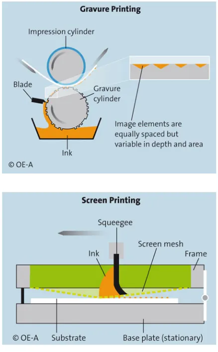
A wide range of large area deposition and patterning techniques can be used for organic electronics. Most prominent in this context are various printing techniques that are well known from the graphic arts industry and enable reel-to-reel pro-cessing. An in-depth analysis of these techniques and their application to organic device manufacturing is given inChap. 2of this book (Konarka).
Examples of two high volume printing processes, gravure and screen, are shown in Figs.1.17and1.18.
Othermass printing processes are offset lithography andflexography. The lateral resolution (smallest feature that can be printed) typically ranges from 20 to 100lm depending on process, throughput, substrate and ink properties, but there
has been recent progress on moving to feature sizes as small as 10lm. Film
thicknesses can range from well under 1 to 10lm. These printing processes can
have enormous throughput and low production cost, but place demanding requirements on the functional inks in terms of properties like viscosity, and
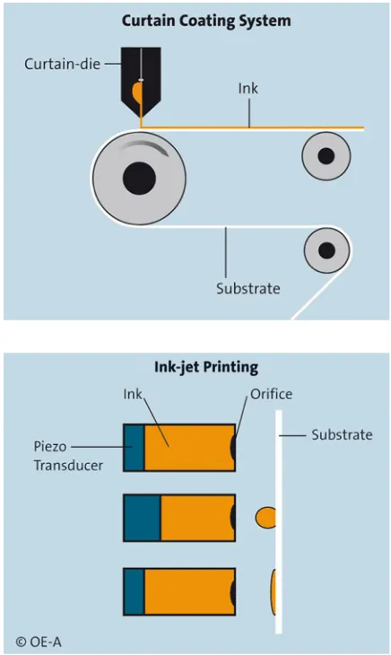
cannot correct for issues like substrate distortion. Mass printing will be an important production process especially for applications where large area, high volumes and low costs are important. Related to volume printing are unpatterned solution coating techniques such as slot-die, wire bar or curtain coating (Fig.1.19).
Ink-jet printinghas received growing interest as a way to deposit functional materials (see Fig.1.20). Being ink-jet a digital printing process, where no printing plate is needed, this technique enables variable printing and can correct in-line for distortions. Ink-jet printing head developers have continued to manufacture finer and finer printing heads, which are starting to enable features on the order of a few
lm, and throughput is improving with the development of multi-head printers. Laser ablation, large area vacuum deposition, soft lithography and large area photolithography are further patterning and deposition techniques. Some of these processes are subtractive, i.e. involve removing unwanted material from a
Fig. 1.17 Gravure printing process.SourceOE-A
large area unpatterned film, while others are additive, i.e. only deposit material where it is wanted. Sub-lm patterning techniques such as nanoimprint lithography
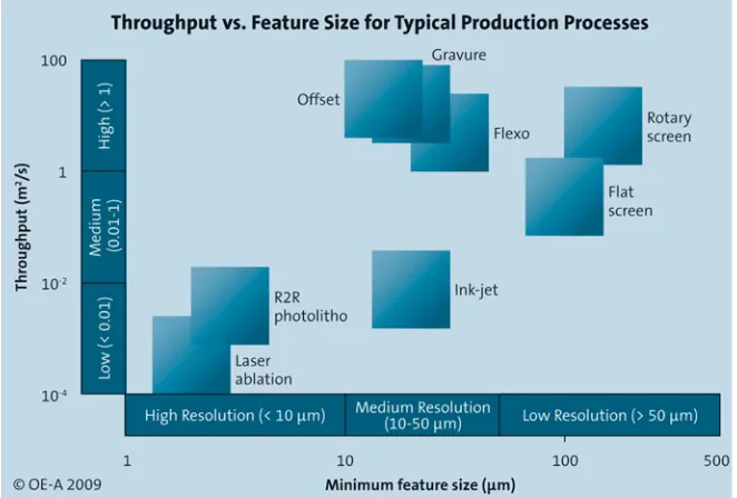
and micro contact printing have gained a good deal of attention recently but are still primarily used in research. Each method has its individual strengths, and in general, processes with a higher resolution have a smaller throughput (Fig.1.21). There are no single standard processes in existence today. Deciding which printing or other patterning process is used depends on the specific requirements of a particular device. In general, different processes have to be used for subsequent steps of a multilayer device in order to optimize each process step. The above mentioned processes differ strongly with regard to e.g. resolution and throughput, and one system may require some high throughput steps followed by high resolution pro-cesses, e.g. deposition of large amounts of material using coating or mass printing followed by fine patterning of a small portion of the surface using laser ablation.
Fig. 1.19 Curtain coating process.SourceCoatema coating machinery
1.3.3 Devices
The organic materials can be combined to a number ofactive componentssuch as transistors, diodes, various types of sensors, memories, photo-voltaic cells, dis-plays or batteries. Examples forpassive devices are conductive traces, antennas, resistors, capacitors or inductors.
Transistorsare a key component of many electronic devices, including RFID or O-TFT backplanes (Organic Thin Film Transistors) for displays, and are a building block for most electrical circuits. An example of the configuration of a typical organic field-effect transistor is shown in Fig.1.22. Essentially, the device consists of four layers: gate electrode, insulator, source/drain electrodes and the semiconductor. The current flow between source and drain electrode is switched, depending on the voltage applied at the gate electrode. In order to optimize the transistor properties, the channel length should be as small as possible and the mobility of the organic semiconductor should be as high as possible.
The other key active components in organic electronics arediodes. These can be large-area devices such as OLEDs based on small molecules or polymers (Fig.1.23) andphotovoltaic cells, or small area components in a circuit. In par-ticular, rectifying diodes are a key component in RF circuits [24] and recently have been demonstrated in display backplanes [25] and memory cells [26] as well. Typically a diode consists of two electrodes (one of them transparent for
photovoltaic cells or OLEDs) and anywhere between one and several organic layers with different functions such as hole or electron transport, light absorption or light emission. More details on organic photovoltaic cells and OLEDs can be found respectively in theChaps. 2(Konarka),3(Samsung), and4(Philips) of this book.
1.3.4 Technology Levels
The technologies that are used in organic electronics range from batch, clean-room, etching based processes to mass printing processes that are capable of deposition of square meters of substrates per second.
Here is a rough classification of the technologies in three different technology levels:
The wafer level technology includes batch processing, typically using film substrates on a carrier. An adapted semiconductor line is used for processing. High
Fig. 1.22 TypicalOFET (organic field-effect transistor) configuration and connections. The thickness of the layer stack is typically below 1lm.SourceOE-A
resolution can be achieved by vacuum deposition and/or spin coating followed by photolithography and wet or dry etching. The production cost is relatively high and the process is not compatible for conversion to in-line sheet to sheet or reel to reel processes.
Underhybridtechnologies, we summarize combinations of processes including large area photolithography, screen printing or printed circuit board (PCB) tech-nologies that make use of flexible substrates (e.g. polymer films or paper). Deposition of materials is by spin coating, doctor blading or large area vacuum deposition, in some cases also partly by printing. Ink-jet printing and laser-pat-terning are further technologies that are grouped in the hybrids and enable pro-duction at a medium cost level.
Fully printedtechnology is the term we use to refer to the use of continuous, automated mass-production compatible printing and coating techniques, flexible substrates and high throughput sheet to sheet or reel-to-reel processing (see Fig.1.24). Although all-printed devices do not yet show as high resolution or performance as those made using wafer or hybrid processes, mass printing has great potential for very low cost production and will be able to deliver extremely large numbers of products. At the same time it requires significant volumes of materials even for trials, and will need large volume applications to properly utilise such high-throughput equipment.
1.3.5 Key Technology Parameters
The detailed application parameter specifications for the different applications and product generations help define the requirements that have to be fulfilled from the technology side. The technology parameters are more ‘‘fundamental’’ and describe fundamental material, device or process properties. As with the application parameters, we only list a small excerpt of the key technology parameters iden-tified for the various applications, focussing on those that are relevant to a number of applications.
• Mobility/electrical performance
(threshold voltage, on/off current ratio)
The performance (operating frequency, current driving capacity) of the circuits depends on parameters like the carrier mobility of the semiconductor and the threshold voltage, the conductivity of the conductor and the dielectrical behaviour of the dielectric materials.
• Resolution/registration
• Barrier properties/environmental stability
The lifetime depends on a combination of the sensitivity of the materials and devices to oxygen and moisture and the barrier properties of protective layers, substrates and sealants against oxygen and moisture. The necessary barrier prop-erties vary for the different applications over several orders of magnitude.
• Flexibility/bending radius
Thin form factors and flexibility of the devices are key advantages of organic electronics. In order to achieve reliable flexible and even roll-able devices mate-rials, design and process have to be chosen carefully.
• Compatibility of process parameters
(speed, temperature, solvents, ambient conditions, vacuum, inert gas atmosphere)
In order for a multi-component system to work properly and be easily manu-facturable, it is important to adjust the parameters of the different materials and devices and choose the right order of processing.
• Yield
Low cost electronics in high volumes are only possible when the processes allow production at high yields. This requires reliable and validated processes, optimised materials and circuit designs as well as an in-line quality control.
1.4 Main Challenges
One goal of the roadmap is to identifyred brick walls—principle challenges that can only be overcome by major breakthroughs beyond the expectations of standard technology development. For each application the requirements for product gen-erations were compared with expected technology development and the key challenges were identified and discussed. Like the key application and technology parameters, the red brick walls may vary for the different applications. Those discussed below are the most important ones and are relevant for all applications. A common feature of all future generations of the different products is that the complexity and overall size of analogue and digital circuitsis increasing. In certain cases, the applications include millions of transistors, other combine var-ious different electronic devices like transistors, power supply, sensors, displays and switches. In the future more and more higher and higher performance com-ponents will have to be fit into smaller and smaller areas, while for other appli-cations high performance components will have to be placed precisely over large areas, up to a few square meters. At the same time, wafer level processing will not in the long term be a commercially viable approach for a number of applications and hybrid or fully printed processes will need to be used.
Based on the above considerations and the results of the work of the application and technology groups, we believe that major breakthroughsin the following areas are absolutely necessary:
resolution, registrationandprocess stabilityof the patterning processes charge carrier mobilityand electrical conductivity of the semiconductor and conducting materials
circuit design and realization of increasingly complex circuits including complementary (analogous to CMOS in Si technology) transistors
These challenges cannot be treated in separate ways since they depend on each other. Resolution and registration accuracy differ for the various patterning tech-niques and even within a technique largely depend on the throughput or printing speed. The process stability depends on tolerable deviation, the circuit design and the materials that are used.
In order to enable mass production of complex devices,resolutionbetter than 10lm with as good or better registration accuracy, even on plastic substrates, is
necessary. Scaling to smaller structures will become important for improved performance and increased yield, as well as to reduce the footprint for the most complex circuits. This cannot be achieved with the current level of development in high throughput, large area processes. At the same time, new strategies forquality controlenabling high speed in-line measurement and electrical testing have to be developed. These developments will be essential to enabling low cost production at high volumes and yield.
commercially available materials would represent a breakthrough since it would enable more complex devices. While such values are starting to be reported on a lab scale, commercial availability could lead to breakthroughs in the industry. Further optimisation of existing materials or development of novel classes of materials will be needed to achieve this. In addition to polymers, potential can-didates include small molecule and inorganic semiconductor materials as well as nanomaterials and new hybrid systems that can be processed from solution.
Another principle challenge is thecircuit designfor complex circuits that are compatible with a broad range of materials and mass printing processes. In par-ticular, complementary circuits need to be developed, which requires high quality p- and n-type semiconductors. This will enable complex circuit designs and will significantly increase functionality of the devices, as it did previously in silicon technology. CMOS analogue design also brings significant advantages in yield, speed and available functions. In addition, designs for lower supply voltages and higher frequencies are of great importance. Progress has been made in this area recently, with gravure printed complementary inverters reported [27] and large European projects aimed at more complex applications of organic complementary circuitry [28], but much still remains to be done.
A key reason to identify red brick walls is to help the organic electronics community align its efforts to solve the most pressing problems. Long-term strategies, funding and new partnerships along the value chain are necessary to overcome the red brick walls.
1.5 Summary and Outlook
Organic and printed electronics is a new and fascinating platform technology that enables fresh electronic applications in many fields, such as interactive toys, RFID-tags, sensors, rollable displays or flexible solar cells, which are now entering the market. With this third version of the OE-A roadmap, we have updated and expanded the information about our view of the developments in this field. We included new applications, updated the status, key parameters and expected technology development for them and used this updated information to identify the key challenges, which we call red brick walls. We have also tried to bring the basic information together to a relatively simple picture of the main developments in this field from the application and technology point of view.
For example, the development of an organic CMOS-like technology could result in a breakthrough of organic electronics, just like it did with silicon elec-tronics. Improved patterning processes and materials with better electrical per-formance and processability are also key for future product generations. It is expected that new organic and inorganic materials will play an important role too. Very important are also the new developments in inline quality control of electrical parameters, especially in printing processes. This will allow sufficiently high yields to reach low cost, high volume products. Standardization in materials, processes and device design gain more and more importance as organic electronics is entering the production phase.
However, some questions remain open; for example we have not yet been able to define a simple ‘‘Moore’s law’’ for organic electronics. Organic electronics is still a very young field, and there are still many different parameters that are important for its further success; it is not clear which of these parameters might have the most important role or how they will scale. However, there are indica-tions that such parameters as charge carrier mobility, feature size and circuit complexity could become candidates for simple scaling laws in the future. We also have not yet been able to identify the ‘‘killer application’’ for organic electronics in the long term; there are many fascinating applications and time will tell which of these—or new ones we have not yet thought of—will turn into a ‘‘killer application’’.
Organic and printed electronics is now in the market and has great potential for further growth. We will continue to follow the developments to find the major trends. The organic electronics roadmap is an ongoing task and key activity of the OE-A and its members, and we will regularly update the roadmap and keep the community informed.
References
1. Clemens W, Lupo D, Hecker K, Breitung S (2009) White Paper OE-A Roadmap for Organic and Printed Electronics. Organic Electronics Association (OE-A).http://www.vdma.org/wps/ myportal/Home/en/Datenbanken/Downloads?WCM_GLOBAL_CONTEXT=/vdma/Home/ en/Datenbanken/Downloads&initsearch=&branche=OEA. Accessed 2011(Since Dec 2011 an updated (4th) edition of the OE-A Roadmap is available at this site.)
2. Menippos GmbH.http://hurrafussball.com/. Accessed 2011
3. Varta Microbatteries GmbH. (http://www.varta-microbatteries.com /en/newsandpr/news_-new/news_new.php?action=detail&id=115). Accessed 2011
4. Konarka Technologies, Inc.www.konarka.com. Accessed 2011 5. G24 Innovations.www.g24i.com. Accessed 2011
6. Koninklijke Philips Electronics N.V.http://www.lighting.philips.com/main/lightcommunity/ trends/oled/. Accessed 2011
7. OSRAM GmbH. http://www.osram.com/osram_com/LED/OLED_Lighting/index.html. Accessed 2011
9. Clemens W, Krumm J, Blache R (2010) Printed RFID and Smart Objects for new high volume applications, Ibidem,Section 6.5
10. Myny K, Beenhakkers MJ, van Aerle NAJM, Gelinck G H, Genoe J, Dehaene W, Heremans P (2009) A 128b Organic RFID Transponder chip, including manchester encoding and ALOHA anti-collision protocol, operating with a data rate of 1529b/s. ISSCC Dig Tech Papers 206–207
11. Genoe J (2008) High frequency rectification for organic RFID tag. Organic Semiconductor Conference 2008, Frankfurt Messe, Frankfurt Germany, 30 Sept 2008
12. Sutija D (2010) Commercialization path for non-volatile rewritable memories—current markets and the pathway to integrated products, LOPE-C 2010, Frankfurt Messe, Frankfurt Germany, 31 May 2010
13. Mildner W (2009) Roadmap for organic and printed electronics. LOPE-C 2009, Frankfurt Messe, Frankfurt Germany, 24 June 2009
14. Interactive Wear AG.http://interactive-wear.de/cms/front_content.php?client=1&changelang =3&parent=&subid=&idcat=72&idart=112. Accessed 2011
15. Brochier Technologies.http://www.brochiertechnologies.com/gb/index.html. Accessed 2011 16. Organic Electronics (2006) 1st edn VDMA Verlag GmbH, Frankfurt am Main, Germany 17. Wikipedia.http://en.wikipedia.org/wiki/PEDOT:PSS. Accessed 2011
18. Wikipedia.http://en.wikipedia.org/wiki/P3HT. Accessed 2011 19. Wikipedia.http://en.wikipedia.org/wiki/Pentacene. Accessed 2011
20. Llorente GR, Dufourg-Madec M-B, Crouch DJ, Pritchard RG, Ogier S, Yeates SG (2009) High performance, acene-based organic thin film transistors. Chem Commun 21:3059 21. Park S-J, Jeong JK, Mo Y-G, Kim S (2009) Impact of high-k TiOx dielectric on device
performance of indium-gallium-zinc oxide transistors. Appl Phys Lett 94:042105 22. KOVIO.http://www.kovio.com/index.html. Accessed 2011
23. Arias AC, Mackenzie JD, Rivnay J, Salleo A (2010) Materials and applications for large area electronics: solution-based approaches. Chem Rev 110:3–24
24. Myny K, Steudel S, Vicca P, Genoe J, Heremans P (2008) An integrated double half-wave organic Schottky diode rectifier on foil operating at 13.56 MHz. Appl Phys Lett 93:093305 25. Lilja KE, Bäcklund TG, Lupo D, Virtanen J, Hämäläinen E, Joutsenoja T (2010) Printed organic diode backplane for matrix addressing an electrophoretic display. Thin Solid Films 518(15):4385–4389
26. Naber RCG, Asadi K, Blom PWM, de Leeuw DM, de Boer B (2010) Organic nonvolatile memory devices based on ferroelectricity. Adv Mater 22:933–945
27. Yan H, Chen Z, Zheng Y, Newman C, Quinn JR, Dötz F, Kastler M, Facchetti A (2009) A high-mobility electron-transporting polymer for printed transistors. Nature 457:679–686 28. POLARIC. http://www.vtt.fi/sites/polaric/ and COSMIC -http://www.project-cosmic.eu/
Chapter 2
Solution-Processed Organic Photovoltaics
Claudia N. Hoth, Pavel Schilinsky, Stelios A. Choulis, Srinivasan Balasubramanian and Christoph J. Brabec
Abstract The technology of organic solar cells has matured to an extent that commercialization of first products has already started. However, with the first products pushing into the market, the research community realizes that a qualified product requires more than only high efficiency and good stability. Cost is of course as important as efficiency and lifetime, but to achieve high productivity, multiple technologic challenges have still to be solved. To reduce production costs, printing of functional layers from solution has evolved to a promising manufacturing technology for flexible organic electronics. Current processing of organic photovoltaic devices is mainly based on traditional methods like spin coating or doctor blading. However, these techniques have several disadvantages such as the incompatibility with a roll-to-roll setup and the processing of only small areas at laboratory scale. Enormous benefits in the manufacturing of organic photovoltaics are achieved by using low-cost roll-to-roll capable technologies including screen printing, spray coating, inkjet printing, gravure/flexographic printing and curtain/slot die coating. This review will shed some light on the role and importance of production technologies for organic photovoltaics and give an update on the most recent achievements in the field.
C. N. Hoth (&)P. Schilinsky
Konarka Technologies GmbH, Landgrabenstrasse 94, 90443 Nürnberg, Germany e-mail: [email protected]
S. A. Choulis
Department of Mechanical Engineering and Materials Science and Engineering, Cyprus University of Technology, 3603 Limassol, Cyprus
S. Balasubramanian
Konarka Technologies Inc., 116 John Street, Lowell, MA 01852, USA C. J. Brabec
Institute Materials for Electronics and Energy Technology (I-MEET), Friedrich-Alexander-University Erlangen-Nürnberg, Martensstr. 7, 91058 Erlangen, Germany
E. Cantatore (ed.),Applications of Organic and Printed Electronics, Integrated Circuits and Systems, DOI: 10.1007/978-1-4614-3160-2_2, Springer Science+Business Media New York 2013
Keywords Organic solar cells
OPVPrintingCoatingPolymerFullerene Bulk heterojunctionDevice fabrication
Lifetime
2.1 Introduction
Amorphous semiconducting polymeric materials have attracted significant interest in the field of organic electronics due to their processing advantages [1–3]. The possibility of applying these materials at low temperatures using solution coating techniques has resulted in intense research activity in recent years. The develop-ments in the fields of organic field effect transistors (OFET or OTFT), organic light emitting diodes (OLED), organic photodetectors and organic photovoltaics (OPV) have now made organic electronics commercially viable. The low-temperature solution processability allows for roll-to-roll printing or coating on flexible plastic substrates which is expected to lead to light-weight, low-cost electronic devices including among others displays, photovoltaic devices and thin film batteries.
For photovoltaics in particular, roll-to-roll production is attractive due to the requirements of low cost, light weight and large area coverage that characterize these products.
Other technologies such as thin film inorganic semiconductor devices that require, for instance, chemical vapour deposition or lithography do not realize the vision of low-cost products due to higher manufacturing cost when compared to printing and coating.
Inorganic bulk semiconductors do not, or only in a very limited way, offer a processing window adequate for solution processing. Inorganic solar cells based on colloidal semiconductor nanocrystals (CdTe and CdSe) spin coated from solution have been presented by the Alivisatos group. These air-stable devices performed well with 2.9 % power conversion efficiencies (PCE) [4]. Inorganic solution-fabricated CIGS (Cu(In,Ga)Se2) cells are being commercialized with over
10 % PCE [5,6], but these materials suffer from complex processing, e.g. high temperature conditions, which do not enable the use of low-cost flexible plastic substrates and roll-to-roll processing. Roll-to-roll vacuum processing of thin film inorganic photovoltaic based on materials like amorphous silicon has also been demonstrated. However, this approach is characterized by much lower throughput and significant higher costs than printing technologies.
In addition to production costs, the competitive position of a photovoltaic technology must be assessed comparing how much efficiency can be gained per spent dollar with the different approaches.
In this chapter we analyze the potential of low-cost printed organic photovol-taics. The challenges associated with large-scale printing or coating procedures are addressed together with an overview of OPV performance in terms of efficiency and operational stability.
interface are the organic material system with the highest reported efficiencies. The working horses for electron donating and accepting materials in the BHJ structure are the well-known poly(3-hexylthiophene) (P3HT) and the C60 derivative PCBM ([6,6]-phenyl-C61-butyric acid methyl ester). The chemical structures of the materials as well as a typical device configuration are shown in Fig.2.1.
For a solar cell at least one transparent electrode is required, which is typically a conductive oxide (TCO). The transparent electrode is often defined by indium tin oxide (ITO) coated on glass or flexible plastic carriers. Together with a thin layer of the intrinsically conductive poly(3,4-ethylene dioxythiophene) doped with the polyanion polystyrene sulfonate (PEDOT:PSS), a high work function hole-col-lecting electrode is built. The photoactive layer is formed by the donor–acceptor blend film, which forms morphologies with phase separation in the nm-scale characterized by good percolation pathways for efficient charge collection and decreased charge recombination. The use of two materials emphasizing different electronic levels is one of the most important design concepts for organic bulk heterojunction solar cells. With this donor–acceptor material combination several groups have reported laboratory device efficiencies in the range of 4 % [7–9]. Low-bandgap benzothiadiazole-fused thiophene copolymers such as poly[2,6-(4,4-bis-(2-ethylhexyl)-4H-cyclopenta [2,1-b;3,4-b’]-dithiophene)-alt -4,7-(2,1,3-ben-zothiadiazole)] (PCPDTBT) used as donor materials represent a promising route to improved device efficiency, due to the better overlap between the PCPDTBT absorption spectrum and the solar emission spectrum [10–14]. A new class of polymer materials which are viable for OPV manufacturing currently give certified performance beyond 8 % [15]. In this chapter, however, we focus our analysis on the well known and widely used P3HT:PCBM blends.
The origin of the open circuit voltage (VOC) is a matter of controversial discus-sions.VOCis the voltage at the terminals of a solar cell when no current flows and is basically determined by the distance between the highest occupied molecular orbital
PCBM P3HT
Photoactive Layer
(HOMO) level of the donor and the lowest unoccupied molecular orbital (LUMO) level of the acceptor material, as shown in Fig.2.2a (indicated as EHL).
Under illumination a photo-induced charge transfer occurs. As the bulk absorbs photon energy, coulombically bound electron–hole-pairs (excitons) are generated, that dissociate at the donor–acceptor interface into electrons and holes. Charge transport to the opposite electrodes takes then place: holes are transported by the p-type material to the higher work function electrode (TCO) and electrons by the n-type material to the lower work function contact (metal), respectively. The short
Energy [eV]
vacuum level (a)
(b)
circuit current density (JSC) depends on the number of photogenerated charges col-lected by the electrodes. The JSC is among others affected by the absorption of photons, the mobility of charge carriers within the active layer, recombination pro-cesses and the morphology of the active layer. The relationship between device efficiency,VOC,JSCand fill factor (FF) is shown in Fig.2.2b on a typicalJ–V char-acteristics under illumination and in the dark. TheFFis defined as the ratio of the actual maximum obtainable power, (Vmp9Jmp) to the maximum theoretical power, (Jsc 9Voc). TheFFis limited by insufficient transport properties, increased series resistanceRsor reduced parallel resistanceRp.RsandRpcan be determined by the inverse of the slope of theJ–Vcharacteristics in the pointsVocandJscrespectively. The performance of BHJ solar cells depends critically on the material properties and processing conditions. Depending on the printing technology the ink must fulfil certain requirements for a reliable printing and adequate film formation in terms of viscosity, boiling point, vapour pressure, polarity and surface tension. The selection of organic solvents is determined by solubility, drying characteristics, fluidity, surface tension and environmental and regulatory considerations. There-fore, the ink is formulated with respect not only to the solvent properties, but also to adapt the ink to the printing technology. The characteristic properties of the different printing methods applied to manufacture solar cells and the requirements on the inks will be extensively discussed in theSect. 2.2.
Section 2.3 will concentrate on reliability and yield aspects of OPVs, while Sect. 2.4will discuss accelerated lifetime test procedures andSect. 2.5will present a possible roadmap for printed solar cells.