Ivan P. Kaminow retired from Bell Labs in 1996 after a 42-year career. He conducted seminal studies on electrooptic modulators and materials, Raman scatter-ing in ferroelectrics, integrated optics, semiconductor lasers (DBR, ridge-waveguide InGaAsP, and multi-frequency), birefringent optical fibers, and WDM networks. Later, he led research on WDM components (EDFAs, AWGs, and fiber Fabry-Perot Filters), and on WDM local and wide area networks. He is a member of the National Academy of Engineering and a recipient of the IEEE/OSA John Tyndall, OSA Charles Townes, and IEEE/LEOS Quantum Electronics Awards. Since 2004, he has been Adjunct Professor of Electrical Engineering at the University of California, Berkeley.
Tingye Li retired from AT&T in 1998 after a 41-year career at Bell Labs and AT&T Labs. His seminal work on laser resonator modes is considered a classic. Since the late 1960s, he and his groups have conducted pioneering studies on lightwave technologies and systems. He led the work on amplified WDM trans-mission systems and championed their deployment for upgrading network capa-city. He is a member of the National Academy of Engineering and a foreign member of the Chinese Academy of Engineering. He is also a recipient of the IEEE David Sarnoff Award, IEEE/OSA John Tyndall Award, OSA Ives Medal/ Quinn Endowment, AT&T Science and Technology Medal, and IEEE Photonics Award.
Optical Fiber Telecommunications V A
Components and Subsystems
Edited by
Ivan P. Kaminow
Tingye Li
Alan E. Willner
AMSTERDAM•BOSTON•HEIDELBERG•LONDON NEW YORK•OXFORD•PARIS•SAN DIEGO SAN FRANCISCO•SINGAPORE•SYDNEY•TOKYO
30 Corporate Drive, Suite 400, Burlington, MA 01803, USA 525 B Street, Suite 1900, San Diego, California 92101-4495, USA 84 Theobald’s Road, London WC1X 8RR, UK
This book is printed on acid-free paper.
Copyright2008, Elsevier Inc. All rights reserved.
No part of this publication may be reproduced or transmitted in any form or by any means, electronic or mechanical, including photocopy, recording, or any information storage and retrieval system, without permission in writing from the publisher.
Permissions may be sought directly from Elsevier’s Science & Technology Rights Department in Oxford, UK: phone: (þ44) 1865 843830, fax: (þ44) 1865 853333, E-mail: [email protected]. You may also complete your request on-line via the Elsevier homepage (http://elsevier.com), by selecting ‘‘Support & Contact’’ then ‘‘Copyright and Permission’’ and then ‘‘Obtaining Permissions.’’
Library of Congress Cataloging-in-Publication Data
Application submitted
British Library Cataloguing-in-Publication Data
A catalogue record for this book is available from the British Library.
ISBN: 978-0-12-374171-4
For information on all Academic Press publications visit our Web site at www.books.elsevier.com
Printed in the United States of America 08 09 10 11 12 8 7 6 5 4 3 2 1
Working together to grow
libraries in developing countries
For Edith, Debbie, and Kathy with Love—TL For Michelle, our Children (Moshe, Asher, Ari, Jacob),
Contributors ix
Chapter 1 Overview of OFT V Volumes A & B 1
Ivan P. Kaminow, Tingye Li, and Alan E. Willner
Chapter 2 Semiconductor Quantum Dots: Genesis—The Excitonic
Zoo—Novel Devices for Future Applications 23
Dieter Bimberg
Chapter 3 High-Speed Low-Chirp Semiconductor Lasers 53 Shun Lien Chuang, Guobin Liu, and Piotr Konrad Kondratko
Chapter 4 Recent Advances in Surface-Emitting Lasers 81 Fumio Koyama
Chapter 5 Pump Diode Lasers 107
Christoph Harder
Chapter 6 Ultrahigh-Speed Laser Modulation by Injection Locking 145 Connie J. Chang-Hasnain and Xiaoxue Zhao
Chapter 7 Recent Developments in High-Speed Optical
Modulators 183
Lars Thyle´n, Urban Westergren, Petter Holmstro¨m, Richard Schatz, and Peter Ja¨nes
Chapter 8 Advances in Photodetectors 221
Joe Charles Campbell
Chapter 9 Planar Lightwave Circuits in Fiber-Optic Communications 269 Christopher R. Doerr and Katsunari Okamoto
Chapter 10 III–V Photonic Integrated Circuits and Their Impact
on Optical Network Architectures 343
Dave Welch, Chuck Joyner, Damien Lambert, Peter W. Evans, and Maura Raburn
Chapter 11 Silicon Photonics 381
Cary Gunn and Thomas L. Koch
Chapter 12 Photonic Crystal Theory: Temporal Coupled-Mode
Formalism 431
Shanhui Fan
Chapter 13 Photonic Crystal Technologies: Experiment 455 Susumu Noda
Chapter 14 Photonic Crystal Fibers: Basics and Applications 485 Philip St John Russell
Chapter 15 Specialty Fibers for Optical Communication Systems 523 Ming-Jun Li, Xin Chen, Daniel A. Nolan, Ji Wang,
James A. West, and Karl W. Koch
Chapter 16 Plastic Optical Fibers: Technologies and Communication
Links 593
Yasuhiro Koike and Satoshi Takahashi
Chapter 17 Polarization Mode Dispersion 605
Misha Brodsky, Nicholas J. Frigo, and Moshe Tur
Chapter 18 Electronic Signal Processing for Dispersion Compensation and Error Mitigation in Optical Transmission Networks 671 Abhijit Shanbhag, Qian Yu, and John Choma
Chapter 19 Microelectromechanical Systems for Lightwave
Communication 713
Ming C. Wu, Olav Solgaard, and Joseph E. Ford
Chapter 20 Nonlinear Optics in Communications: From Crippling
Impairment to Ultrafast Tools 759
Stojan Radic, David J. Moss, and Benjamin J. Eggleton
Chapter 21 Fiber-Optic Quantum Information Technologies 829 Prem Kumar, Jun Chen, Paul L. Voss, Xiaoying Li,
Kim Fook Lee, and Jay E. Sharping
Dieter Bimberg, Institut fuer Festkoerperphysik and Center of Nanophotonics, Berlin, Germany, [email protected]
Misha Brodsky, AT&T Labs – Research, Middletown, NJ, USA, [email protected]
Joe Charles Campbell, School of Engineering and Applied Science, Department of Electrical and Computer Engineering, University of Virginia, Charlottesville, VA, USA, [email protected]
Connie J. Chang-Hasnain, Department of Electrical Engineering and Computer Sciences, University of California, Berkeley, CA, USA, [email protected]
Jun Chen, Center for Photonic Communication and Computing, EECS Department, Northwestern University, Evanston, IL, USA Xin Chen, Corning Inc., Corning, NY, USA, [email protected] John Choma, Scintera Inc., Sunnyvale, CA, USA, [email protected] Shun Lien Chuang, Department of ECE, University of Illinois, Urbana, IL, USA, [email protected]
Christopher R. Doerr, Alcatel-Lucent, Holmdel, NJ, USA, [email protected]
Benjamin J. Eggleton, ARC Centre of Excellence for Ultrahigh-bandwidth Devices for Optical Systems (CUDOS), School of Physics, University of Sydney, Australia, [email protected]
Peter W. Evans, Infinera Inc., Sunnyvale, CA, USA, [email protected] Shanhui Fan, Ginzton Laboratory, Department of Electrical Engineering, Stanford, CA, USA, [email protected]
Joseph E. Ford, Department of Electrical and Computer Engineering, University of California, San Diego, CA, USA, [email protected]
Nicholas J. Frigo, Department of Physics, U.S. Naval Academy, Annapolis, MD, USA, [email protected]
Cary Gunn, Chief Technology Officer, Luxtera, Inc., Carlsbad, CA, USA, [email protected]
Christoph Harder, HPP, Etzelstrasse 58, Schindellegi, Switzerland, [email protected]
Petter Holmstro¨m, Department of Microelectronics and Applied Physics, Royal Institute of Technology (KTH), Kista, Sweden, [email protected] Peter Ja¨nes, Proximion Fiber Systems AB, Kista, Sweden,
Chuck Joyner, Infinera Inc., Sunnyvale, CA, USA, [email protected] Ivan P. Kaminow, 254M Cory Hall #1770, University of California, Berkeley, CA, USA, [email protected]
Karl W. Koch, Corning Inc., Corning, NY, USA, [email protected] Thomas L. Koch, Center for Optical Technologies, Sinclair Laboratory, Lehigh University, Bethlehem, PA, USA, [email protected]
Yasuhiro Koike, Keio University ERATO Koike Photonics Polymer Project, Yokohama, Japan, [email protected]
Piotr Konrad Kondratko, Department of ECE, University of Illinois, Urbana, IL, USA, [email protected]
Fumio Koyama, Microsystem Research Center, P&I Lab, Tokyo Institute of Technology, Nagatsuta, Midori-ku, Yokohama, Japan,
Prem Kumar, Technological Institute, Northwestern University, Evanston, IL, USA, [email protected]
Damien Lambert, Infinera Inc., Sunnyvale, CA, USA, [email protected] Kim Fook Lee, Center for Photonic Communication and Computing,
Xiaoying Li, Center for Photonic Communication and Computing, EECS Department, Northwestern University, Evanston, IL, USA
Guobin Liu, Department of ECE, University of Illinois, Urbana, IL, USA, [email protected]
David J. Moss, ARC Centre of Excellence for Ultrahigh-bandwidth Devices for Optical Systems (CUDOS), School of Physics, University of Sydney, Australia, [email protected]
Susumu Noda, Department of Electronic Science and Engineering, Kyoto University, Kyoto, Japan, [email protected]
Daniel A. Nolan, Corning Inc., Corning, NY, USA, [email protected] Katsunari Okamoto, Okamoto Laboratory, 2-1-33 Higashihara, Mito-shi, Ibaraki-ken, 310-0035, Japan, [email protected]
Maura Raburn, Infinera Inc., Sunnyvale, CA, USA, [email protected] Stojan Radic, Department of Electrical and Computer Engineering,
University of California, San Diego, La Jolla, CA, USA, [email protected] Philip St. John Russell, Max-Planck Research Group (IOIP), University of Erlangen-Nuremberg, Erlangen, Germany, [email protected] Richard Schatz, Department of Microelectronics and Applied Physics, Royal Institute of Technology (KTH), Kista, Sweden, [email protected] Abhijit Shanbhag, Scintera Inc., Sunnyvale, CA, USA, [email protected] Jay E. Sharping, University of California, Merced, CA,
Olav Solgaard, Department of Electrical Engineering, Edward L. Ginzton Laboratory, Stanford University, Stanford, CA, USA, [email protected] Satoshi Takahashi, The Application Group, Shin-Kawasaki Town Campus, Keio University, Kawasaki, Japan, [email protected]
Lars Thyle´n, Department of Microelectronics and Applied Physics, Royal Institute of Technology (KTH), Kista, Sweden, [email protected] Moshe Tur, School of Electrical Engineering, Tel Aviv University, Ramat Aviv, Israel, [email protected]
Ji Wang, Corning Inc., Corning, NY, USA, [email protected] Dave Welch, Infinera Inc., Sunnyvale, CA, USA, [email protected] James A. West, Corning Inc., Corning, NY, USA, [email protected] Urban Westergren, Department of Microelectronics and Applied Physics, Royal Institute of Technology (KTH), Kista, Sweden, [email protected] Alan E. Willner, Ming Hsieh Department of Electrical Engineering, Viterbi School of Engineering, University of Southern California, Los Angeles, CA, USA, [email protected]
Ming C. Wu, Berkeley Sensor and Actuator Center (BSAC) and Electrical Engineering & Computer Science Department, University of California, Berkeley, CA, USA, [email protected]
Qian Yu, Scintera Inc., Sunnyvale, CA, USA, [email protected]
1
Overview of OFT V volumes A & B
Ivan P. Kaminow
*, Tingye Li
†, and Alan E. Willner
‡*
University of California, Berkeley, CA, USA
†
Boulder, CO, USA
‡
University of Southern California, Los Angeles, CA, USA
Optical Fiber Telecommunications V (OFT V)is the fifth installment of theOFT
series. Now 29 years old, the series is a compilation by the research and devel-opment community of progress in optical fiber communications. Each edition reflects the current state-of-the-art at the time. As Editors, we started with a clean slate of chapters and authors. Our goal was to update topics fromOFT IVthat are still relevant as well as to elucidate topics that have emerged since the last edition.
1.1 FIVE EDITIONS
Installments of the series have been published roughly every 6–8 years and chronicle the natural evolution of the field:
• In the late 1970s, the original OFT (Chenoweth and Miller, 1979) was concerned with enabling a simple optical link, in which reliable fibers, connectors, lasers, and detectors played the major roles.
• In the late 1980s,OFT II(Miller and Kaminow, 1988) was published after the first field trials and deployments of simple optical links. By this time, the advantages of multiuser optical networking had captured the imagination of the community and were highlighted in the book.
• OFT III(Kaminow and Koch, 1997) explored the explosion in transmission
capacity in the early-to-mid 1990s, made possible by the erbium-doped fiber amplifier (EDFA), wavelength division multiplexing (WDM), and dispersion management.
Optical Fiber Telecommunications V A: Components and Subsystems
Copyright2008, Elsevier Inc. All rights reserved.
• By 2002,OFT IV(Kaminow and Li, 2002) dealt with extending the distance
and capacity envelope of transmission systems. Subtle nonlinear and disper-sive effects, requiring mitigation or compensation in the optical and electrical domains, were explored.
• The present edition ofOFT, V,(Kaminow, Li, and Willner, 2008) moves the series into the realm of network management and services, as well as employ-ing optical communications for ever-shorter distances. Usemploy-ing the high band-width capacity in a cost-effective manner for customer applications takes center stage. In addition, many of the topics from earlier volumes are brought up to date; and new areas of research which show promise of impact are featured.
Although each edition has added new topics, it is also true that new challenges emerge as they relate to older topics. Typically, certain devices may have ade-quately solved transmission problems for the systems of that era. However, as systems become more complex, critical device technologies that might have been considered a “solved problem” previously have new requirements placed upon them and need a fresh technical treatment. For this reason, each edition has grown in sheer size, i.e., adding the new and, if necessary, reexamining the old.
An example of this circular feedback mechanism relates to the fiber itself. At first, systems simply required low-loss fiber. However, long-distance transmission enabled by EDFAs drove research on low-dispersion fiber. Further, advances in WDM and the problems of nonlinear effects necessitated development of nonzero dispersion fiber. Cost considerations and ultra-high-performance systems, respectively, are driv-ing research in plastic fibers and ultra-low-polarization-dependent fibers. We believe that these cycles will continue. Each volume includes a CD-ROM with all the figures from that volume. Select figures are in color. The volume B CD-ROM also has some supplementary Powerpoint slides to accompany Chapter 19 of that volume.
1.2 PERSPECTIVE OF THE PAST 6 YEARS
Our field has experienced an unprecedented upheaval since 2002. Theirrational
exuberance and despair of the technology “bubble-and-bust” had poured untold sums of money into development and supply of optical technologies, which was followed by a depression-like period of over supply. We are happy to say that, by nearly all accounts, the field is gaining strength again and appears to be entering a stage ofrationalgrowth.
growth rate, which generated enthusiasm and demand, leading to unsustainable expectations. Could such a discontinuity happen again? Perhaps, but chastened investors now seem to be following a more gradual and sensible path. Throughout the “bubble-and-bust” until the present, the actual demand for bandwidth has grown at a very healthy 80% per year globally; thus, real traffic demand experienced no bubble at all. The growth and capacity needs are real, and should continue in the future.
As a final comment, we note that optical fiber communications is firmly entrenched as part of the global information infrastructure. The only question is how deeply will it penetrate and complement other forms of communications, e.g., wireless, access, and on-premises networks, interconnects, satellites, etc. This prospect is in stark contrast to the voice-based future seen byOFT,published in 1979, before the first commercial intercontinental or transatlantic cable systems were deployed in the 1980s. We now have Tb/s systems for metro and long-haul networks. It is interesting to contemplate what topics and concerns might appear in
OFT VI.
1.3 OFT V VOLUME A: COMPONENTS
AND SUBSYSTEMS
1.3.1 Chapter 1. Overview of OFT V volumes A & B
(
Ivan P. Kaminow, Tingye Li, and Alan E. Willner
)
This chapter briefly reviews herewith all the chapters contained in both volumes of OFT V.
1.3.2 Chapter 2. Semiconductor quantum dots:
Genesis—The Excitonic Zoo—novel devices
for future applications (
Dieter Bimberg
)
1.3.3 Chapter 3. High-speed low-chirp semiconductor lasers
(
Shun Lien Chuang, Guobin Liu, and Piotr Konrad
Kondratko
)
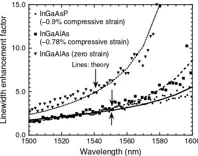
One advantage of using quantum wells and quantum dots for the active region of lasers is the lower induced chirp when such lasers are directly modulated, permit-ting direct laser modulation that can save on the cost of separate external modulators. This chapter provides a comparison of InAlGaAs with InGaAsP long-wavelength quantum-well lasers in terms of high-speed performance, and extracts the important parameters such as gain, differential gain, photon lifetime, temperature dependence, and chirp. Both DC characteristics and high-speed direct modulation of quantum-well lasers are presented, and a comparison with theore-tical models is made. The chapter also provides insights into novel quantum-dot lasers for high-speed operation, including the ideas of p-type doping vs tunneling injection for broadband operation.
1.3.4 Chapter 4. Recent advances in surface-emitting lasers
(
Fumio Koyama
)
Vertical cavity surface-emitting lasers (VCSELs) have a number of special proper-ties (compared with the more familiar edge-emitting lasers) that permit some novel applications. This chapter begins with an introduction which briefly surveys recent advances in VCSELs, several of that are then treated in detail. These include techniques for realizing long-wavelength operation (as earlier VCSELs were limited to operation near 850 nm), the performance of dense VCSEL arrays that emit a range of discrete wavelengths (as large as 110 in number), and MEMS-based athermal VCSELs. Also, plasmonic VCSELs that produce subwavelength spots for high-density data storage and detection are examined. Finally, work on all-optical signal processing and slow light is presented.
1.3.5 Chapter 5. Pump diode lasers (
Christoph Harder
)
This chapter details the many lessons learned in the design for manufacture of commercial pump lasers in the two bands. Based on the performance developed for telecom, numerous other commercial applications for high-power lasers have emerged in manufacturing and printing; these applications are also discussed.
1.3.6 Chapter 6. Ultrahigh-speed laser modulation by
injection locking (
Connie J. Chang-Hasnain and
Xiaoxue Zhao
)
It has been known for decades that one oscillator (the slave) can be locked in frequency and phase to an external oscillator (the master) coupled to it. Current studies of injection-locked lasers show that the dynamic characteristics of the directly modulated slave are much improved over the same laser when freely running. Substantial improvements are found in modulation bandwidth for analog and digital modulation, in linearity, in chirp reduction and in noise performance.
In this chapter, theoretical and experimental aspects of injection locking in all lasers are reviewed with emphasis on the authors’ research on VCSELs (vertical cavity surface-emitting lasers). A recent promising application in passive optical networks for fiber to the home (FTTH) is also discussed.
1.3.7 Chapter 7. Recent developments in high-speed
optical modulators (
Lars Thyle´n, Urban Westergren,
Petter Holmstro¨m, Richard Schatz, and Peter Ja¨nes
)
Current high-speed lightwave systems make use of electro-optic modulators based on lithium niobate or electroabsorption modulators based on semiconductor materi-als. In commercial systems, the very high-speed lithium niobate devices often require a traveling wave structure, while the semiconductor devices are usually lumped.
This chapter reviews the theory of high-speed modulators (at rates of 100 Gb/s) and then considers practical design approaches, including comparison of lumped and traveling-wave designs. The main emphasis is on electroabsorption devices based on Franz–Keldysh effect, quantum-confined Stark effect and intersubband absorption. A number of novel designs are described and experimental results given.
1.3.8 Chapter 8. Advances in photodetectors
(
Joe Charles Campbell
)
were developed and commercialized for systems that operated at 1.3- and 1.5-mm wavelengths, albeit the avalanche photodiodes (APDs) were expensive and nonideal. Introduction of erbium-doped fiber amplifiers and WDM technology in the 1990s relegated APDs to the background, as p–i–n photoreceivers performed well in amplified systems, whereas APDs were plagued by the amplified spontaneous emission noise. Future advanced systems and special applications will require sophisticated devices involving deep understanding of device physics and technology. This chapter focuses on three primary topics: high-speed waveguide photodiodes for systems that operate at 100 Gb/s and beyond, photodiodes with high saturation current for high-power applica-tions, and recent advances of APDs for applications in telecommunications.
1.3.9 Chapter 9. Planar lightwave circuits in fiber-optic
communications (
Christopher R. Doerr and
Katsunari Okamoto
)
The realization of one or more optical waveguide components on a planar substrate has been under study for over 35 years. Today, individual components such as splitters and arrayed waveguide grating routers (AWGRs) are in widespread commercial use. Sophisticated functions, such as reconfigurable add–drop multiplexers (ROADMs) and high-performance filters, have been demonstrated by integrating elaborate combinations of such components on a single chip. For the most part, these photonic integrated circuits (PICs), or planar lightwave circuits (PLCs), are based on passive waveguides in lower index materials, such as silica.
This chapter deals with the theory and design of such PICs. The following two chapters (Chapters 11 and 12) also deal with PICs; however, they are designed to be integrated with silicon electronic ICs, either in hybrid fashion by short wire bonds to an InP PIC or directly to a silicon PIC.
1.3.10 Chapter 10. III–V photonic integrated circuits
and their impact on optical network architectures
(
Dave Welch, Chuck Joyner, Damien Lambert, Peter
W. Evans, and Maura Raburn
)
InP-based semiconductors are unique in their capability to support all the photonic components required for wavelength division multiplexed (WDM) transmitters and receivers in the telecom band at 1550 nm. Present subsystems have connected these individual components by fibers or lenses to form hybrid transmitters and receivers for each channel.
economically viable for deployment in commercial WDM systems. The photonic integrated circuits are wire-bonded to adjacent silicon ICs. Thus a single board provides optoelectronic regeneration for 10 channels, dramatically reducing interconnection complexity and equipment space. In addition, as in legacy single-channel systems, the “digital” approach for transmission (as compared to “all-optical”) offers ease of network monitoring and management. This chapter covers the technology of InP photonic integrated circuits (PICs) and their commercial application. The impact on optical network architecture and operation is discussed and technology advances for future systems are presented.
1.3.11 Chapter 11. Silicon photonics (
Cary Gunn
and Thomas L. Koch
)
Huge amounts of money have been invested in silicon processing technology, thanks to a steady stream of applications that justified the next stage of proces-sing development. In addition to investment, innovative design, process disci-pline and large-volume runs made for economic success. The InP PICs described in the previous chapter owe their success to lessons learned in silicon IC processing.
Many people have been attracted by the prospects of fabricating PICs using silicon alone to capitalize on the investment and success of silicon ICs. To succeed one requires a large-volume application and a design that can be made in an operating silicon IC foundry facility. A further potential advantage is the oppor-tunity to incorporate on the same photonic chip electronic signal processing. The application to interconnects for high-performance computers is a foremost motiva-tion for this work.
While silicon has proven to be the ideal material for electronic ICs, it is far from ideal for PICs. The main shortcoming is the inability so far to make a good light source or photodetector in silicon. This chapter discusses the successes and challenges encountered in realizing silicon PICs to date.
1.3.12 Chapter 12. Photonic crystal theory: Temporal
coupled-mode formalism (
Shanhui Fan
)
designed using such a material with a photonic bandgap and, subsequently, introducing line and point defect states into the gap. Various functional devices, such as filters, switches, modulators and delay lines, can be created by control-ling the coupcontrol-ling between these defect states. This chapter reviews the temporal coupled-mode theory formalism that provides the theoretical foundation of many of these devices.
1.3.13 Chapter 13. Photonic crystal technologies:
Experiment (
Susumu Noda
)
Photonic crystals belong to a class of optical nanostructures characterized by the formation of band structures with respect to photon energy. In 3D photonic crystals, a complete photonic band gap is formed; the presence of light with frequencies lying in the band gap is not allowed. This chapter describes the application of various types of materials engineering to photonic crystals, with particular focus on the band gap/defect, the band edge, and the transmission band within each band structure. The manipulation of photons in a variety of ways becomes possible. Moreover, this chapter discusses the recent introduction of “photonic heterostructures” as well as recent developments concerning two- and three-dimensional photonic crystals.
1.3.14 Chapter 14. Photonic crystal fibers: Basics
and applications (
Philip St John Russell
)
Photonic crystal fibers (PCFs)—fibers with a periodic transverse microstructure— first emerged as practical low-loss waveguides in early 1996. The initial demon-stration took 4 years of technological development, and since then the fabrication techniques have become more and more sophisticated. It is now possible to manufacture the microstructure in air–glass PCFs to accuracies of 10 nm on the scale of 1mm, which allows remarkable control of key optical properties such as dispersion, birefringence, nonlinearity and the position and width of the photonic band gaps (PBGs) in the periodic “photonic crystal” cladding. PCF has in this way extended the range of possibilities in optical fibers, both by improving well-established properties and introducing new features such as low-loss guidance in a hollow core.
1.3.15 Chapter 15. Specialty fibers for optical
communication systems (
Ming-Jun Li, Xin Chen,
Daniel A. Nolan, Ji Wang, James A. West, and
Karl W. Koch
)
Specialty fibers are designed by changing fiber glass composition, refractive index profile, or coating to achieve certain unique properties and functionalities. Some of the common specialty fibers include active fibers, polarization control fibers, dispersion compensation fibers, highly nonlinear fibers, coupling or bridge fibers, high-numerical-aperture fibers, fiber Bragg gratings, and special single mode fibers. In this chapter, the design and performance of various specialty fibers are discussed. Special attention is paid to dispersion compensation fibers, polarization-maintaining and single-polarization fibers, highly nonlinear fibers, double clad fiber for high-power lasers and amplifiers, and photonic crystal fibers. Moreover, there is a brief discussion of the applications of these specialty fibers.
1.3.16 Chapter 16. Plastic optical fibers: Technologies
and communication links (
Yasuhiro Koike and
Satoshi Takahashi
)
Plastic optical fiber (POF) consists of a plastic core that is surrounded by a plastic cladding of a refractive index lower than that of the core. POFs have very large core diameters compared to glass optical fibers, and yet they are quite flexible. These features enable easy installation and safe handling. Moreover, the large-core fibers can be connected without high-precision accuracy and with low cost. POFs have been used extensively in short-distance datacom applications, such as in digital audio interfaces. POFs are also used for data transmission within equipment and for control signal transmission in machine tools. During the late 1990s, POFs were used as the transmission medium in the data bus within automobiles. As we move into the future, high-speed communication will be required in the home, and POFs are a promising candidate for home network wiring. This chapter describes the POF design and fabrication, the specific fiber properties of attenuation, band-width and thermal stability, and various communications applications, concluding with a discussion of recent developments in graded-index POFs.
1.3.17 Chapter 17. Polarization mode dispersion (
Misha
Brodsky, Nicholas J. Frigo, and Moshe Tur
)
theorists, experimentalists, network designers, field engineers and, during the “bubble” years, entrepreneurial technologists. A comprehensive treatment of the subject up to year 2002 is given in a chapter bearing the same title inOptical Fiber
Telecommunications IVB, System and Impairments. The present chapter is an
overview of PMD with special emphasis on the knowledge accumulated in the past 5 years. It begins with a review of PMD concepts, and proceeds to consider the “hinge” model used to describe field test results, which are presented and analyzed. The important subject of system penalties and outages due to first-order PMD is then examined, followed by deliberations of higher-order PMD, and interaction between fiber nonlinear effects and PMD.
1.3.18 Chapter 18. Electronic signal processing for
dispersion compensation and error mitigation in
optical transmission networks (
Abhijit Shanbhag,
Qian Yu, and John Choma
)
Dispersion equalization has its origin in the early days of analog transmission of voice over copper wires where loading coils (filters) were distributed in the net-work to equalize the frequency response of the transmission line. Digital transmis-sion over twisted pairs was enabled by the invention of the transversal equalizer which extended greatly the bandwidth and reach. Sophisticated signal processing and modulation techniques have now made mobile telephones ubiquitous. How-ever, it was not until the mid 1990s that wide deployment of Gigabit Ethernet rendered silicon CMOS ICs economical for application in high-speed lightwave transmission. Most, if not all lightwave transmission systems deployed today, use electronic forward error correction and dispersion compensation to alleviate signal degradation due to noise and fiber dispersive effects.
This chapter presents an overview of various electronic equalization and adap-tation techniques, and discusses their high-speed implemenadap-tation, specifically addressing 10-Gb/s applications for local-area, metro, and long-haul networks. It comprises a comprehensive survey of the role, scope, limitations, trends, and challenges of this very important and compelling technology.
1.3.19 Chapter 19. Microelectromechanical systems for
lightwave communication (
Ming C. Wu, Olav
Solgaard, and Joseph E. Ford
)
elements may be called for in some applications. Either a free-space or integrated layout may be used.
This chapter describes the recent lightwave system applications of MEMS. In telecommunications, MEMS switches can provide cross-connects with large numbers of ports. A variety of wavelength selective devices, such as reconfigurable optical add–drop multiplexers (ROADM) employ MEMS. More recent devices include tunable lasers and microdisk resonators.
1.3.20 Chapter 20. Nonlinear optics in communications:
from crippling impairment to ultrafast tools (
Stojan
Radic, David J. Moss, and Benjamin J. Eggleton
)
It is perhaps somewhat paradoxical that optical nonlinearities, whilst having posed significant limitations for long-haul WDM systems, also offer the promise of addres-sing the bandwidth bottleneck for signal procesaddres-sing for future optical networks as they evolve beyond 40 Gb/s. In particular, all-optical devices based on the 3rd order
(3)optical nonlinearity offer a significant promise in this regard, not only because the intrinsic nonresonant (3) is nearly instantaneous, but also because (3) is responsible for a wide range of phenomena, including 3rd harmonic generation, stimulated Raman gain, four-wave mixing, optical phase conjugation, two-photon absorption, and the nonlinear refractive index. This plethora of physical processes has been the basis for a wide range of activity on all-optical signal processing devices. This chapter focuses on breakthroughs in the past few years on approaches based on highly nonlinear silica fiber as well as chalcogenide-glass-based fiber and waveguide devices. The chapter contrasts two qualitatively different approaches to all-optical signal processing based on nonphase-matched and phase-matched pro-cesses. All-optical applications of 2R and 3R regeneration, wavelength conver-sion, parametric amplification, phase conjugation, delay, performance monitoring, and switching are reviewed.
1.3.21 Chapter 21. Fiber-optic quantum information
technologies (
Prem Kumar, Jun Chen, Paul L. Voss,
Xiaoying Li, Kim Fook Lee, and Jay E. Sharping
)
can only exist in one of two deterministic states (i.e., “heads” or “tails”), and not something in between. In other words, the individual particle in quantum entangle-ment does not have a well-defined pure state before measureentangle-ment.
Since the beginning of the 1990s, the field of quantum information and com-munication has expanded rapidly, with quantum entanglement being a critical aspect. Entanglement is still an unresolved “mystery,” but a new world of “quantum ideas” has been ignited and is actively being pursued. The focus of this chapter is the generation of correlated and entangled photons in the telecom band using the Kerr nonlinearity in dispersion-shifted fiber. Of particular interest are microstructure fibers, in which tailorable dispersion properties have allowed phase-matching and entanglement to be obtained over a wide range of wavelengths.
1.4 OFT V VOLUME B: SYSTEMS AND NETWORKS
1.4.1 Chapter 1. Overview of OFT V volumes A & B
(
Ivan P. Kaminow, Tingye Li, and Alan E. Willner
)
This chapter briefly reviews herewith all the chapters contained in both volumes of OFT V.
1.4.2 Chapter 2. Advanced optical modulation formats
(
Peter J. Winzer and Rene´-Jean Essiambre
)
Today, digital radio-frequency (rf) communication equipment employs sophisti-cated signal processing and communication theory technology to realize amazing performance; wireless telephones are a prime example. These implementations are made possible by the capabilities and low cost of silicon integrated circuits in high-volume consumer applications. Some of these techniques, such as forward error correction (FEC) and electronic dispersion compensation (EDC) are currently in use in lightwave communications to enhance signal-to-noise ratio and mitigate signal degradation. (See the chapter on “Electronic Signal Processing for Disper-sion Compensation and Error Mitigation in Optical TransmisDisper-sion Networks” by Abhijit Shanbhag, Qian Yu, and John Choma.) Advanced modulation formats that are robust to transmission impairments or able to improve spectral efficiency are being considered for next-generation lightwave systems.
1.4.3 Chapter 3. Coherent optical communication systems
(
Kazuro Kikuchi
)
The first generation of single-channel fiber optic networks used on-off keying and direct detection. Later, coherent systems, employing homodyne and heterodyne detection, were intensely researched with the aim of taking advantage of their improved sensitivity and WDM frequency selectivity. However, the quick success of EDFAs in the 1990s cut short the prospects for coherent systems.
Now, interest in coherent is being renewed as the need for greater spectral effi-ciency in achieving greater bandwidth per fiber has become apparent. This chapter reviews the theory of multilevel modulation formats that permit multiple bits/s of data per Hz of bandwidth. (See the chapter on “Advanced Modulation Formats” by Winzer and Essiambre.) The growing capabilities of silicon data signal processing (DSP) can be combined with digital coherent detection to provide dramatic improvements in spectral efficiency. Experimental results for such receivers are presented.
1.4.4 Chapter 4. Self-coherent optical transport systems
(
Xiang Liu, Sethumadhavan Chandrasekhar, and
Andreas Leven
)
As stated above, coherent detection transmission systems were investigated in the 1980s for their improved receiver sensitivity and selectivity, and for the promise of possible postdetection dispersion compensation. However, the emergence of EDFAs and amplified WDM systems relegated the technically difficult coherent technology to the background. Now, as high-speed signal processing technology becomes technically and economically feasible, there is renewed interest in studying coherent and self-coherent systems, especially for their capability to increase spectral efficiency through the use of advanced multilevel modulation techniques and, more important, for the possibility of implementing postdetection equalization functionalities.
Self-coherent systemsutilize differential direct detection that does not require a
local oscillator. With high-speed analog-to-digital conversion and digital signal processing, both phase and amplitude of the received optical field can be recon-structed, thus offering unprecedented capability for implementing adaptive equaliza-tion of transmission impairments. This chapter is a comprehensive and in-depth treatment of self-coherent transmission systems, including theoretical considerations, receiver technologies, modulation formats, adaptive equalization techniques, and applications for capacity upgrades and cost reduction in future optical networks.
1.4.5 Chapter 5. High-bit-rate ETDM transmission
systems (
Karsten Schuh and Eugen Lach
)
observation has prompted the telecom industry to develop higher-speed systems for upgrading transport capacity. Indeed, there is a relentless drive to explore higher speed for multichannel amplified WDM transmission where, for a given speed of operation, the total system cost is roughly proportional to the number of channels plus a fixed cost. It is important to note that the cost of equalizing for signal impairment at higher speeds must be taken into account.
This chapter is an up-to-date review of high-speed transmission using electronic time division multiplexing (ETDM), a time-honored approach for upgrading system capacity. The emphasis is on 100-Gb/s bit rate and beyond, as 40-Gb/s systems are already being deployed and 100-Gb/s Ethernet (100 GE) is expected to be the next dominant transport technology. The chapter includes a basic treatment of ETDM technology, followed by a description of the concepts of high-speed ETDM systems. Requirements of optical and electronic components and the state-of-the-art technologies are then examined in detail, and an up-to-date overview of ultra-high-speed systems experiments is presented. Finally, prospects of the var-ious approaches for rendering cost-effective 100 GE are contemplated.
1.4.6 Chapter 6. Ultra-high-speed OTDM transmission
technology (
Hans-Georg Weber and Reinhold Ludwig
)
The expected increase of transmission capacity in optical fiber networks will involve an optimized combination of WDM and TDM. TDM may be realized by electrical multiplexing (ETDM) or by optical multiplexing (OTDM). Dispersion impairment notwithstanding, OTDM offers a means to increase the single-channel bit rate beyond the capability of ETDM. Thus OTDM transmission technology is often considered to be a research means with which to investigate the feasibility of ultra-high-speed transmission. Historically, the highest speed commercial systems have been ETDM systems. Latest examples are 40 G systems being deployed at present and (serial) 100 G systems expected to be commercially available in a few years. In the past 10 years, OTDM transmission technology has made considerable progress towards much higher bit rates and much longer transmission links.
This chapter discusses ultra-high-speed data transmission in optical fibers based on OTDM technology. The chapter gives a general description of an OTDM system, the OTDM transmitter, the OTDM receiver, and the fiber transmission line. WDM/OTDM transmission experiments are also described.
1.4.7 Chapter 7. Optical performance monitoring
(
Alan E. Willner, Zhongqi Pan, and Changyuan Yu
)
higher-capacity systems, since network paths are not static and channel-degrading effects can change with temperature, component drift, aging and fiber plant maintenance. In order to enable robust and cost-effective automated operation, the network should be able to: (i) intelligently monitor the physical state of the network as well as the quality of propagating data signals, (ii) automatically diagnose and repair the network, and (iii) redirect traffic. To achieve this, optical performance monitoring should isolate the specific cause of the problem. Further-more, it can be quite advantageous to determine when a data signal is beginning to degrade, so that the network can take action to correct the problem or to route the traffic around the degraded area.
This chapter explores optical performance monitoring and its potential for enabling higher stability, reconfigurability, and flexibility in an optical network. Moreover, this chapter describes the specific parameters that a network might want to monitor, such as chromatic dispersion, polarization-mode dispersion, and opti-cal SNR. Promising monitoring techniques are reviewed.
1.4.8 Chapter 8. ROADMs and their system applications
(
Mark D. Feuer, Daniel C. Kilper, and Sheryl L.
Woodward
)
As service providers begin to offer IPTV services in addition to data and voice, the need for fast and flexible provisioning of mixed services and for meeting unpre-dictable traffic demand becomes compelling. Reconfigurable optical add/drop multiplexers (ROADMs) have emerged as the network element that can satisfy this need. Indeed, subsystem and system vendors are rapidly developing and producing ROADMs, and carriers are installing and deploying them in their networks.
This chapter is a comprehensive treatment of ROADMs and their application in WDM transmission systems and networks, comprising a review of various ROADM technologies and architectures; analyses of their routing functionalities and economic advantages; considerations of design features and other requirements; and discussions of the design of ROADM transmission systems and the interplay between the ROADM and transmission performance. The chapter ends with some thoughts on the remaining challenges to enable ROADMs to achieve their potential.
1.4.9 Chapter 9. Optical Ethernet: Protocols, management,
and 1–100 G technologies (
Cedric F. Lam and
Winston I. Way
)
networks, and for next-generation long-haul networks. As stated concisely by the authors, “The success of Ethernet is attributed to its simplicity, low cost, standard implementation, and interoperability guarantee,” attributes that helped the “networking community it serves to prosper, hence producing the economy of scale.” This chapter is an in-depth review of the evolution and development of Ethernet technology for application in optical fiber telecommunications networks. Topics covered include: point-to-point Ethernet development, Layer-2 functions, Carrier Ethernet, Ethernet in access PONs, Ethernet OAM (Operation, Administration, Maintenance), development of 10 GE for PON and 100 GE for core applications, and examples of high-speed Ethernet.
1.4.10 Chapter 10. Fiber-based broadband access
technology and deployment (
Richard E. Wagner
)
One of the earliest long-haul commercial optical fiber telecom systems was the AT&T Northeast Corridor link from Boston to New York to Washington in 1983. In this application, the large capital investment could be amortized among many users. The prospect of economically bringing fiber all the way to a large number of end users, where cost sharing is not available, has continuously appealed to and challenged the telecom industry. Presently, technology advances and volume manufacture are reducing costs/user, fabulous broadband applications are luring subscribers, and government legislation and subsidies are encouraging growth worldwide. This chapter tracks the history of broadband access, compares the competing access technologies, and projects the roadmap to future deployment in the US, Asia, Europe and the rest of the world. The economic driver for widespread deployment is the explosive growth of Internet traffic, which doubles annually in developed countries and grows even faster in developing countries, such as China. In developed countries, growth is due to new broadband applications; in developing countries, both new users and new applications drive traffic growth.
This chapter focuses on the fiber-based approaches to broadband access worldwide, including some of the drivers for deployment, the architectural options, the capital and operational costs, the technological advances, and the future potential of these systems. Three variants of fiber-based broadband access, collectively called FTTx in this chapter, have emerged as particularly important. They are: hybrid-fiber-coax (HFC) systems, fiber-to-the-cabinet (FTTC) systems, and fiber-to-the-home (FTTH) systems.
1.4.11 Chapter 11. Global landscape in broadband:
Politics, economics, and applications (
Richard Mack
)
operational costs in dollars per unit bandwidth (per unit distance). For metro, regional, and long-haul arenas, lightwave technology is indisputably the king. However, in the access arena, the competitive unit cost of lightwave technology has not favored rational deployment. Indeed, the history of FTTH has followed a tortuous path; the early trials in the 1980s and 1990s did not lead to massive deployment. Globally, Japanese and Korean telecom com-panies have been leading the installation of FTTH (with as yet unknown eco-nomic consequences). In the meantime, the cost of FTTH equipment has been decreasing steadily. Recently, relief from “unbundling” (exemption from requirement for incumbent carriers to share facilities with competitive carriers, as ruled by FCC) and competition from cable TV companies have prompted incumbent carriers in the US to install FTTH with competitive (triple-play) service offerings. As the demand for broadband services grows and revenue improves, the return from the vast investment in FTTH may be realized in the not-to-distant future.
This chapter is a fascinating, data-laden account of the history of deployment of optical fiber telecommunications, with emphasis on economics, growth landscape, and broadband services in the access arena. The discussion includes historical highlights, demographics, costs and revenues, fiber installations, services scenar-ios, competition and growth, regulatory policies, applications and bandwidth requirements, technology and network architecture choices, market scenarios, etc. The interplay of these issues is discussed and summarized in the concluding section.
1.4.12 Chapter 12. Metro networks: Services and
technologies (
Loukas Paraschis, Ori Gerstel,
and Michael Y. Frankel
)
Metropolitan networks operate in the environs of a major city, transporting and managing traffic to meet the diverse service needs of enterprise and residential applications. Typically, metro networks have a reach below a few hundred kilometers with node traffic capacities and traffic granularity that require amplified dense WDM technology with optical add/drop, although the more economical coarse WDM technology has also been deployed. At present, convergence of IP services and traditional time-division multiplexed (TDM) traffic with low operational cost is an important issue.
1.4.13 Chapter 13. Commercial optical networks, overlay
networks, and services (
Robert Doverspike and
Peter Magill
)
As service providers are the ultimate users of novel technologies and systems in their networks, it is important that the innovators have a sound understanding of the structure and workings of the carriers’ networks: the architecture and layers, traffic and capacity demands, management of reliability and services, etc. Com-mercial networks are continuously upgraded to provide more capacity, new ser-vices and reduced capital and operational cost; seamless network evolution is essential for obvious economic reasons. Even when “disruptive” technologies and platforms are introduced, smooth integration within the existing infrastructure is imperative.
This chapter reviews the important aspects of current commercial optical networks in all three segments or layers: access, metro, and core. Topics include 1. relationship of services to layers, covering service requirements, layer tech-nology, quality of service, Service Level Agreements, network availability, and network restoration; and 2. network and services evolution, covering demand and capacity, and applications and technologies in all three segments of the network. In the summary section, the authors point out that while much of the “industry focuses on advanced optical technologies for the long-distance net-work, most of the investment and opportunity for growth resides in the metro/ access [sector].”
1.4.14 Chapter 14. Technologies for global telecommunications
using undersea cables (
Se´bastien Bigo
)
The introduction of WDM has enabled a tremendous capacity growth in undersea systems, both by the increase in the number of carrier wavelengths and by the increase in the channel bit rate. Starting from 2.5 Gbit/s in the mid-1990s, the bit rate was upgraded in commercial products to 10 Gbit/s at the end of the last century. The next generation of undersea systems will likely be based on 40-Gbit/s bit-rate channels. However, transmission at 40 Gbit/s is significantly more chal-lenging than at 10 Gbit/s.
1.4.15 Chapter 15. Future optical networks
(
Michael O’Mahony
)
In the past few years Internet traffic, doubling annually, has dominated the network capacity demand, which has been met by the advances in lightwave communications. The transformation from a circuit-switched, voice-centric to a packet-switched, IP-centric network is well underway; amplified WDM transmission systems with terabits-per-second capacity are being deployed; rapid reconfigurable networking and automatic service provisioning are being implemented. The drive to reduce cost and increase revenue has being inexorable. In the meantime, carriers are installing FTTH and offering IPTV services, which will undoubtedly change network traffic charac-teristics and boost the traffic growth rate. What will the future networks look like?
This chapter reviews the growth of the data traffic and evolution of the optical network, including user communities, global regional activities, and service requirements. Discussions cover the diversity of architectures, the evolution of switching, cross-connecting and routing technologies, and the transformation to carrier-grade (100 G) Ethernet. The author notes that device integration “will enable the realization of many of the key functionalities for optical networking.”
1.4.16 Chapter 16. Optical burst and packet switching
(
S. J. Ben Yoo
)
Optical switching has the potential of providing more-efficient and higher-through-put networking than its electronic counterpart. This chapter discusses optical burst and packet switching technologies and examines their roles in future optical net-works. It covers the roles of optical circuit, burst, and packet switching systems in optical networks, as well as their respective benefits and trade-offs. A description is given of the networking architecture/protocols, systems, and technologies pertaining to optical burst and packet switching. Furthermore, this chapter introduces optical-label switching technology, which provides a unified platform for interoperating optical circuit, burst, and packet switching techniques. By exploiting contention resolution in wavelength, time, and space domains, the optical-label switching routers can achieve high-throughput without resorting to a store-and-forward method associated with large buffer requirements. Testbed demonstrations in sup-port of multimedia and data communications applications are reviewed.
1.4.17 Chapter 17. Optical and electronic technologies
for packet switching (
Rodney S. Tucker
)
switching, which provides statistical multiplexing of the many data streams that pass through a given switch node. A key element of any packet switch is the ability to buffer (or store) packets temporarily to avoid collisions. Since it is easy to store bits as electronic charge in silicon, commercial packet switches are electronic.
This chapter introduces the basics of practical packet routers, indicating the requirements of a switch based on either electronics or photonics. The author compares the physical limits on routers based on storing and switching electrons vs photons. While many in the optics field would like to see photonic switches dominate, it appears that the physical inability to provide a large optical random access buffer means that packet switches will continue to be optoelectronic rather than all-optical for some time.
1.4.18 Chapter 18. Microwave-over-fiber systems
(
Alwyn J. Seeds
)
The low-loss, wide-bandwidth capability of optical transmission systems makes them attractive for the transmission and processing of microwave signals, while the development of high-capacity optical communication systems has required the import of microwave techniques in optical transmitters and receivers. These two strands have led to the development of the research area of microwave photonics. Following a summary of the historic development of the field and the development of microwave photonic devices, systems applications in telecommunications, and likely areas for future development are discussed. Among the applications reviewed are wireless-over-fiber access systems, broadband signal distribution and access systems, and communications antenna remoting systems.
1.4.19 Chapter 19. Optical interconnection networks in
advanced computing systems (
Keren Bergman
)
This chapter is a review of the subject of interconnection networks for high-performance computers. Performance issues including latency, bandwidth and power consumption are first presented, followed by discussions of design con-siderations including technology, topology, packet switching nodes, message structure and formation, performance analysis, and evaluation. Network design implementation, architectures, and system demonstrations are then covered and thoughts are offered on future directions, including optical interconnection net-works on a chip.
1.4.20 Chapter 20. Simulation tools for devices, systems,
and networks (
Robert Scarmozzino
)
The ability of optical fiber telecommunications to satisfy the enormous demand for network capacity comes from thorough understanding of the physics and other disciplines underlying the technology, as well as the abilities to recognize sources for limitation, develop ideas for solution, and predict, test, and demonstrate those ideas. The field of numerical modeling has already been an important facilitator in this process, and its influence is expected to increase further as photonics matures. This chapter discusses the broad scope of numerical modeling and specifically describes three overarching topics: (i) active and passive device/component-level modeling with emphasis on physical behavior, (ii) transmission-system-level modeling to evaluate data integrity, and (iii) network-transmission-system-level modeling for evaluating capacity planning and network protocols. The chapter offers an over-view of selected numerical algorithms available to simulate photonic devices, communication systems, and networks. For each method, the mathematical formulation is presented along with application examples.
ACKNOWLEDGMENTS
We wish sincerely to thank Tim Pitts and Melanie Benson of Elsevier for their gracious and invaluable support throughout the publishing process. We are also deeply grateful to all the authors for their laudable efforts in submitting their scholarly works of distinction. Finally, we owe a debt of appreciation to the many people whose insightful suggestions were of great assistance.
2
Semiconductor quantum dots:
Genesis—The Excitonic Zoo—novel
devices for future applications
Dieter Bimberg
Institut fuer Festkoerperphysik and Center of Nanophotonics,
Berlin, Germany
2.1 PREFACE
Decisive for the development of civilization of mankind across the last ten thousand years was the discovery, development, and use of novel materials and technologies. Replacing stone by bronze and bronze by iron enabled new tools like the plough, stimulating quantum leaps in agriculture, and handicraft. The informa-tion age started with the discovery and use of silicon—a rather new material when measuring time in bits of a thousand years.
Our knowledge of properties of elements occurring in nature is almost com-plete. The laws of physics governing the interactions of atoms to form liquids or solids with composition-dependent properties are established to a large extent. Still, new materials based on chemical architecture will continue in the future to present the basics of quantum leaps for many new technologies.
By entering now the nanoage, developing nanotechnologies, we realize that size and shape is more than just another subject of researchers’ curiosity in ultrasmall and beautiful objects. Nanotechnologies enable us to modify the properties of semiconductors to a large extentwithoutchanging the composition.
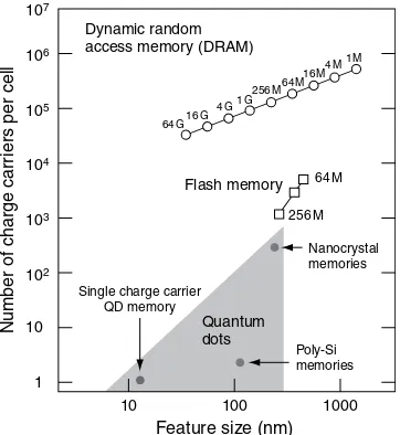
The ultimate class of semiconductor nanostructures, “quantum dots” (QDs), have lateral dimensions in all three directions that are smaller than the de-Broglie-wavelength. They constitute nanometer-size coherent clusters that are embedded in the dielectric matrix of another semiconductor. They are often self-similar and can be formed by self-organized growth on surfaces.Single or fewQDs enable novel devices for quantum cryptography, quantum information processing, and novel DRAM (Dynamic Random Access Memory)/flash memory cells.Billionsof them present the active centers in optoelectronic devices like QD lasers or QD
Optical Fiber Telecommunications V A: Components and Subsystems
Copyright2008, Elsevier Inc. All rights reserved.
optical amplifiers, revolutionizing communication, consumer electronics, mea-surement techniques, and more.
2.2 THE PREHISTORIC ERA—OR WHY DID
A PROMISING APPROACH ALMOST DIE
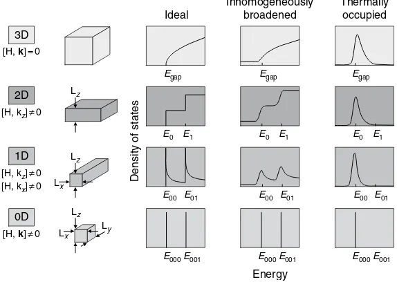
Besides fundamental interest in novel effects, semiconductor research is strongly driven by the prospect of potential applications. The dawn of nanotechnology in semiconductor physics as well as in optoelectronics is closely related to the work of two physicists working at Bell Labs in Murray Hill, USA. Ray Dingle and Charles Henry [1] applied for a patent on quantum well (QW) lasers in 1976. Here, they listed the benefits of reducing the dimensionality of the active area of a semicon-ductor laser when changing from a three-dimensional double heterostructure (three-dimensional structure) to a QW (two-(three-dimensional structure) and finally to a quantum wire structure (1D structure). Such a reduction in dimensionality heavily affects the electronic properties of the respective semiconductor (e.g., GaAs in AlGaAs) as demonstrated in Figure 2.1. Both the energy eigenvalues and the density of states become a function of the lateral dimension inx-,y-, andz-direction.
The density of states of a single QD is given by a-function which, even when occupied by carriers and at high temperatures, does not show thermal broadening. One-, two-, and three-dimensional structures do show such broadening due to the continuous energy dispersion. The threshold current density of a laser was predicted by Dingle and Henry to be drastically lowered when the dimensionality of the active region is reduced. Indeed, today 95% of the semiconductor lasers produced utilize a QW as an active region. Without such already sophisticated QW structures, the penetration of semiconductor lasers to such diverse fields like optical drives, barcode scanners, printers, or telecommunication would not have been possible.
process used for device fabrication, including epitaxial growth, two-dimensional lithography, dry etching (all on a nanometer scale!), overgrowth, and additional processing steps, led to a high density of “lethal” defects. Consequently, the quantum efficiency was very low and the modal gain was insufficient. After many such discouraging reports, some theorists started to warn proceeding to work on low-dimensional structures for photonic devices. The low-quantum efficiency was claimed to be inherent to such structures, resulting from orthogonal electron and hole wave functions, and slow carrier capture and relaxation times of more than nanoseconds [6]. The latter effect was referred to as “phonon bottleneck” and attracted attention of many scientists for a decade. Thus, the nanoscientists started to fundamentally question the new field of nanosemiconductor physics and its technologies.
2.3 A NEW DAWN AND COLLECTIVE BLINDNESS
Surface physicists classify the growth modes for the coherent deposition of material 1 on material 2 (Figure 2.2) into three groups. For close to identical lattice constants, a
Ideal 3D
2D
1D
0D
[H, k]=0
[H, kz]≠0
[H, kz]≠0
[H, kx]≠0
[H, k]≠0 L Ly x
Lz Lx
Lz
Lz
Egap
E0
E00
E000E001 E000E001 E000E001
E01 E00 E01 E00 E01
E1 E0 E1 E0 E1
Egap Egap
Inhomogeneously broadened
Energy
Density of states
Thermally occupied
Figure 2.1The impact of changes of dimensionality on the electronic density of states in a semiconductor
(schematical). In a three-dimensional (volume) semiconductor, the wave vectorkis a good quantum number
two-dimensional growth (monolayer by monolayer) occurs that is called “Frank–van der Merwe” growth mode. This mode is observed, for example, for growth of GaAs on AlGaAs. In case of different lattice constants, the layers of the different materials are strained. When reaching a critical layer thickness of the newly deposited layer, the strain energy is reduced by the formation of defects, in particular of dislocations. An alternative way to minimize strain energy, which was originally disregarded, is the self-organized growth ofcoherentthree-dimensional clusters. Depending on a com-plex interplay of volume energies and orientation-dependent energy contributions by surfaces and edges, the clusters form directly on the substrate (“Volmer–Weber” growth mode) or on a wetting layer with a typical thickness of one to two monolayers (“Stranski–Krastanow” growth mode) [4, 7]. Stranski and Krastanow introduced this universal growth mode on a meeting of the Vienna Academy of Sciences in 1937.
Already in 1985 Goldstein et al. [8] reported on electron microscopy investiga-tions of InAs/GaAs heterostructures that revealed vertically correlated InAs nanoclus-ters. However, they were lacking information on the electronic properties of these clusters and presented no information on whether these clusters were free of defects. A proof of defect-free growth of such structures was given 5 years later by Madhukar et al. [9] at the University of Southern California and Sasaki et al. [10] at the University of Kyoto. Still, there was no experimental evidence for a delta-like density of states in QDs (see Figure 2.1) and no novel or superior device utilizing QDs was demonstrated. Therefore, the reports [8–10] received little attention for a long time.
2.4 DECISIVE BREAK-THROUGHS
In 1994/1995, we reported four break-throughs that prepared the ground for the subsequent explosion of research on semiconductor nanostructures.
• Cathodoluminescence investigations by Marius Grundmann et al. [11]
revealed the delta-function-like emission characteristics of excitons in InAs/GaAs QDs. The samples were grown by molecular beam expitaxy (MBE) at the Ioffe Institute in St Petersburg by Victor Ustinov and Nicolai Ledentsov. Similar observations were reported using photoluminescence by Moison et al. [12] and Petroff et al. [13].
(a) (b) (c)
• Vitali Shchukin et al. [14] developed a theoretical model for the self-similarity
of QD sizes and shapes and for the self-organized growth based on thermo-dynamical arguments [4, 7]. The model also explained the observations reported in Refs [12, 13]. Brilliant high-resolution transmission electron micro-graphs of InAs/GaAs QDs (Figure 2.3) that were grown by Heinrichsdorff et al. [15] using metalorganic chemical vapor deposition (MOCVD) revealed indeed a close to perfect self-similarity of QDs and confirmed Shchukins thermodynamic approach. Further important theoretical work included kinetic aspects [16] and contributed to a more detailed understanding of QD growth.
• Efficient carrier capture into QDs on a picosecond time scale was demonstrated by
Heitz et al. [17] by time-resolved and resonant photoluminescence spectroscopy.
• Nils Kirstaedter et al. [18] succeeded in producing the first injection laser based
on coherently grown QDs. Two theoretically predicted properties of QD lasers of fundamental importance were confirmed by this work: reduced threshold current density and improved temperature stability of the threshold current.
2.5 PARADIGM CHANGES IN SEMICONDUCTOR
PHYSICS AND TECHNOLOGY
The abrupt change of fundamental, technological, and physical paradigms that were not questioned for decades led to an out-bursting development of the research on zero-dimensional structures for the years after 1994:
• Lattice-mismatched semiconductors have to be used for the epitaxial
growth of defect-free QD structures to initiate strain-driven self-organization.
100nm [100]
Such QD formation is observed for almost all IV/IV-, III/V-, and II/VI-heterostructures that meet the conditions. One of the underlying processes of formation is the “Stranski–Krastanow” growth mode; spinoidal decom-position or submonolayer (SML) dedecom-position are other ones [7].
• Charge carriers and excitons are strongly localized in real space for QD
volumes smaller than 103nm3.
• There is no conservation of the wave vectorkin zero-dimensional
struc-tures. Consequently, there is no polarization bottleneck like for structures of higher dimensionality.
• The energy levels of charge carriers or excitons in single dots are discrete like
in atoms, showing homogeneous (Lorentzian) broadening depending on tem-perature only.
• Recombination/absorption and gain are purely (bi)-excitonic.
• Carrier capture, relaxation, and recombination at low temperatures or for
strong confinement have to be described by master equations of micro-states [19]. A global Fermi level is nonexistent.
Figure 2.1 displays the density of states for three-, two-, one-, and zero-dimensional systems. When inhomogeneous broadening and thermal occupation are included, the unique properties of zero-dimensional systems as compared to systems of higher dimensionality are visualized best. All higher dimensional systems resemble each other qualitatively. Zero-dimensional systems are distinct: QDs resemble giant atoms in a dielectric cage more than solids.
2.6 ANYTHING SPECIAL ABOUT THE ELECTRONIC
AND OPTICAL PROPERTIES?
Shape and composition of QDs can be revealed by combining transmission electron microscopy and scanning tunneling microscopy (plane view and cross-section). For determining the precise distribution of atoms in a strained QD, one needs sophisticated algorithms to treat the micrographs based, for example, on molecular dynamical calculations [20].
Once the material distribution inside and outside a QD is known, one can calculate the strain field by, for example, continuum theory or the valence-force-field method [21]. Detailed knowledge of the strain field allows for the determination of piezoelectric potentials and finally for the calculation of the electronic struc-ture using a numerical 8-band k.p model [21]. Alternative methods include empirical pseudopotential calculations as well as tight-binding approaches. Figure 2.4 gives the energy levels and wave functions in a pyramidal InAs/GaAs QD of 13.3 nm base length as obtained by our 8-band k.p model.