ABSTRAK
Teknologi berkembang dengan pesat dari waktu ke waktu, salah satunya
adalah pengendalian on/off secara otomatis. Dengan adanya pengendali on/off
secara otomatis ini, maka pekerjaan manusia dapat menjadi lebih mudah.
Pada tugas akhir ini telah dibuat suatu pengendali on/off melalui
mikrokontroler dengan menggunakan sensor suhu, cahaya dan PIR. Pada
prinsipnya, sensor akan mengirim data ke mikrokontroler, sedangkan keluaran
dari mikrokontroler dihubungkan dengan lampu, kipas angina, dan alarm. Sensor
yang digunakan adalah photodiode sebagai sensor cahaya, LM35 sebagai sensor
suhu, dan PIR sebagai sensor gerak. Untuk mengkonversikan tegangan analog
(input tegangan) dari LM35 menjadi data digital digunakan ADC0804.
Pengujian yang dilakukan mendapat hasil, jika intensitas cahaya ruangan
≤
80 lux, maka lampu akan menyala, sedangkan jika > 80 lux maka lampu akan
padam. Untuk suhu, jika suhu antara 25°C - 28°C, maka kipas akan berputar
lambat, 29°C - 34°C kipas akan berputar sedang, sedangkan 35°C - 40°C kipas
berputar cepat. Untuk PIR yang berfungsi sebagai sensor gerak, jika ada gerakan
yang terdeteksi maka akan menghasilkan tegangan 5V dan alarm berbunyi,
ABSTRACT
Technology expand swiftly from time to time. One of its application is
controller on/off automatically. With existence of on controller / off automatically
this, work of human being can become easierly.
In this final project have been made a controller on/off through the
microcontroller using temperatrure censor, light, and PIR. In principle, censor will
send data to microcontroller, and then output from microcontroller will be
connected to lamp, fan, and alarm. The censor which used are photodiode as light
censor, LM35 as temperature censor and PIR as motion censor. For converting
analog voltage from LM35 to digital data used ADC0804.
Examination conducted get result, if room light intensity less than equal 80
lux else lamp is going to on, than if more than 80 lux else lamp is going to off. For
temperature, if temperature between 25°C - 28°C, else fan will rotate with low
speed, 29°C - 34°C else fan will rotate with medium speed, 29°C - 34°C else fan
will rotate with fast speed. For PIR which used as motion censor, if there a motion
which detected, else will be get a voltage 5V and the alarm sound on, if there are
DAFTAR ISI
ABSTRAK... i
ABSTRACT... ii
KATA PENGANTAR... iii
DAFTAR ISI... v
DAFTAR GAMBAR... vii
DAFTAR TABEL... viii
BAB I :
PENDAHULUAN... 1
1.1. Latar
Belakang...
1
1.2. Identifikasi
Masalah...
1
1.3. Tujuan...
1
1.4. Pembatasan
Masalah...
2
1.5.
Sistematika Penulisan... 2
BAB II :
TEORI PENUNJANG... 4
2.1. Pengendali
mikro
(microcontroller) AT89C51... 4
2.1.1.
Organisasi memori………... 6
2.1.1.1. Program memori………... 7
2.1.1.2. Data memori………...7
2.1.2.
Interupsi... 9
2.1.3.
Metoda Pengalamatan…... 10
2.1.4.
Perangkat Instruksi…... 12
2.2. Photodioda……….13
2.3.
Operational Amplifier……... 13
2.3.1.
Penguat Non Inverting... 15
2.3.2.
Penguat Inverting………... 16
2.4. Infra
Merah………….………...
17
2.5. Prinsip
Kerja
Relay…….………... 21
BAB III :
PERANCANGAN dan REALISASI... 23
3.1.
Diagram Blok dan Spesifikasi Kerja Sistem... 23
3.2. Rangkaian
Catu
Daya…..…...………..
23
3.3.
Perancangan Photodioda.………... 24
3.4.
Perancangan Rangkaian Sensor Suhu.………... 25
3.5.
Perancangan PIR (Passive Infra Red)…….………. 26
3.6.
Rangkaian Mikrokontroler ………... 27
3.7.
Perancangan Perangkat Lunak.…..………... 30
BAB IV :
DATA PENGAMATAN dan ANALISA... 33
4.1.
Pengujian Sensor... 33
4.1.1.
Sensor Photodioda..………... 33
4.1.2.
Sensor Suhu…….………... 34
4.1.3.
Sensor PIR (Passive Infra Red)... 36
4.2.
Pengujian Keseluruhan Sistem…... 36
BAB V :
KESIMPULAN DAN SARAN...38
5.1.
Kesimpulan... 38
5.2.
Saran... 38
DAFTAR PUSTAKA
DAFTAR GAMBAR
Gambar 2.1
Konfigurasi pin pengendali mikro AT89C51... 5
Gambar 2.2 Peta Program Memori Pengendali Mikro AT89C51…... 7
Gambar 2.3 Peta Data memori Pengendali Mikro AT89C51... 8
Gambar 2.4 Simbol Photodioda……... 13
Gambar 2.5 Simbol Op – Amp……... 14
Gambar 2.6 Rangkaian Ekivalen Op-Amp ...…... 14
Gambar 2.7 Penguat Non Inverting dengan Feedback Resistif ... 16
Gambar 2.8 Rangkaian inverting..………....…... 17
Gambar 2.9 Komunikasi Infra Merah……...…... 17
Gambar 2.10 Daerah Frekuensi Gelombang Infra Merah... 18
Gambar 2.11 Daerah Panjang Gelombang Infra Merah... 18
Gambar 2.12 Konstruksi Relay………... 21
Gambar 2.13 Gambar ADC………... 22
Gambar 3.1 Diagram Blok Sistem………... 23
Gambar 3.2 Rangkaian Catu Daya 5 Volt...……... 24
Gambar 3.3 Rangkaian Photodioda ……….…... 24
Gambar 3.4 Rangkaian LM35…………..…………... 26
Gambar 3.5 Daerah Jangkauan PIR (Passive Infra Red)………... 27
Gambar 3.6
Rangkaian Pembangkit Pulsa ………... 27
Gambar 3.7
Rangkaian Manual Reset.……… 28
Gambar 3.8
Rangkaian Mikrokontroler AT89C51.……….…….…………... 29
Gambar 3.9
Flowchart Utama …………..…….………..….………... 31
DAFTAR TABEL
Tabel 2.1 Alamat Layanan Rutin Interupsi... 9
Tabel 4.1 Hasil Pengukuran Photodioda…………... 33
Tabel 4.2 Hasil Pengkuran LM35……….……….. 34
Tabel 4.3 Hasil Keluaran ADC (Analog To Digital Converter)... 35
Tabel 4.4 Hasil Pengkuran PIR (Passive Infra Red)...35
LM35
Precision Centigrade Temperature Sensors
General Description
The LM35 series are precision integrated-circuit temperature sensors, whose output voltage is linearly proportional to the Celsius (Centigrade) temperature. The LM35 thus has an advantage over linear temperature sensors calibrated in ˚ Kelvin, as the user is not required to subtract a large con-stant voltage from its output to obtain convenient Centigrade scaling. The LM35 does not require any external calibration or trimming to provide typical accuracies of±1⁄4˚C at room
temperature and±3⁄4˚C over a full −55 to +150˚C
tempera-ture range. Low cost is assured by trimming and calibration at the wafer level. The LM35’s low output impedance, linear output, and precise inherent calibration make interfacing to readout or control circuitry especially easy. It can be used with single power supplies, or with plus and minus supplies. As it draws only 60 µA from its supply, it has very low self-heating, less than 0.1˚C in still air. The LM35 is rated to operate over a −55˚ to +150˚C temperature range, while the LM35C is rated for a −40˚ to +110˚C range (−10˚ with im-proved accuracy). The LM35 series is available packaged in
hermetic TO-46 transistor packages, while the LM35C, LM35CA, and LM35D are also available in the plastic TO-92 transistor package. The LM35D is also available in an 8-lead surface mount small outline package and a plastic TO-220 package.
Features
n Calibrated directly in ˚ Celsius (Centigrade) n Linear + 10.0 mV/˚C scale factor n 0.5˚C accuracy guaranteeable (at +25˚C) n Rated for full −55˚ to +150˚C range n Suitable for remote applications n Low cost due to wafer-level trimming n Operates from 4 to 30 volts n Less than 60 µA current drain n Low self-heating, 0.08˚C in still air n Nonlinearity only±1⁄4˚C typical
n Low impedance output, 0.1Ωfor 1 mA load
Typical Applications
TRI-STATE®is a registered trademark of National Semiconductor Corporation.
DS005516-3
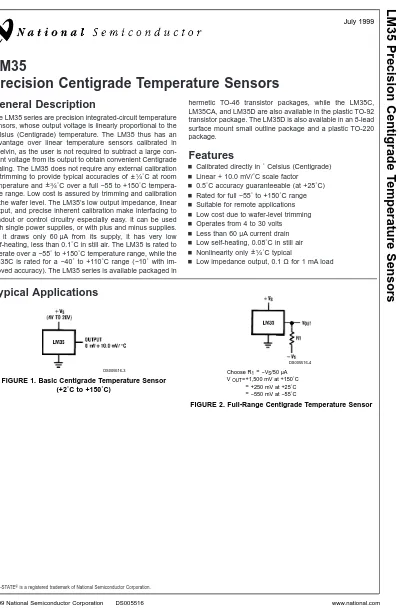
FIGURE 1. Basic Centigrade Temperature Sensor (+2˚C to +150˚C)
DS005516-4
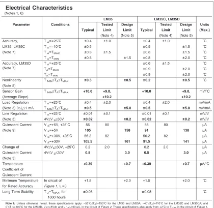
Choose R1= −VS/50 µA VOUT=+1,500 mV at +150˚C
= +250 mV at +25˚C = −550 mV at −55˚C
FIGURE 2. Full-Range Centigrade Temperature Sensor
July 1999
LM35
Precision
Centigrade
T
emperature
Connection Diagrams
TO-46 Metal Can Package*
DS005516-1
*Case is connected to negative pin (GND)
Order Number LM35H, LM35AH, LM35CH, LM35CAH or LM35DH
See NS Package Number H03H
TO-92 Plastic Package
DS005516-2
Order Number LM35CZ, LM35CAZ or LM35DZ See NS Package Number Z03A
SO-8
Small Outline Molded Package
DS005516-21
N.C. = No Connection
Top View Order Number LM35DM See NS Package Number M08A
TO-220 Plastic Package*
DS005516-24
*Tab is connected to the negative pin (GND).
Note: The LM35DT pinout is different than the discontinued LM35DP. Order Number LM35DT
Absolute Maximum Ratings
(Note 10)If Military/Aerospace specified devices are required, please contact the National Semiconductor Sales Office/ Distributors for availability and specifications.
Supply Voltage +35V to −0.2V
Output Voltage +6V to −1.0V
Output Current 10 mA
Storage Temp.;
TO-46 Package, −60˚C to +180˚C
TO-92 Package, −60˚C to +150˚C
SO-8 Package, −65˚C to +150˚C
TO-220 Package, −65˚C to +150˚C
Lead Temp.: TO-46 Package,
(Soldering, 10 seconds) 300˚C
TO-92 and TO-220 Package,
(Soldering, 10 seconds) 260˚C
SO Package (Note 12)
Vapor Phase (60 seconds) 215˚C
Infrared (15 seconds) 220˚C
ESD Susceptibility (Note 11) 2500V
Specified Operating Temperature Range: TMINto TMAX
(Note 2)
LM35, LM35A −55˚C to +150˚C
LM35C, LM35CA −40˚C to +110˚C
LM35D 0˚C to +100˚C
Electrical Characteristics
(Notes 1, 6)LM35A LM35CA
Parameter Conditions Tested Design Tested Design Units Typical Limit Limit Typical Limit Limit (Max.)
(Note 4) (Note 5) (Note 4) (Note 5)
Accuracy TA=+25˚C ±0.2 ±0.5 ±0.2 ±0.5 ˚C
(Note 7) TA=−10˚C ±0.3 ±0.3 ±1.0 ˚C
TA=TMAX ±0.4 ±1.0 ±0.4 ±1.0 ˚C
TA=TMIN ±0.4 ±1.0 ±0.4 ±1.5 ˚C
Nonlinearity TMIN≤TA≤TMAX ±0.18 ±0.35 ±0.15 ±0.3 ˚C
(Note 8)
Sensor Gain TMIN≤TA≤TMAX +10.0 +9.9, +10.0 +9.9, mV/˚C
(Average Slope) +10.1 +10.1
Load Regulation TA=+25˚C ±0.4 ±1.0 ±0.4 ±1.0 mV/mA
(Note 3) 0≤IL≤1 mA TMIN≤TA≤TMAX ±0.5 ±3.0 ±0.5 ±3.0 mV/mA
Line Regulation TA=+25˚C ±0.01 ±0.05 ±0.01 ±0.05 mV/V
(Note 3) 4V≤VS≤30V ±0.02 ±0.1 ±0.02 ±0.1 mV/V
Quiescent Current VS=+5V, +25˚C 56 67 56 67 µA
(Note 9) VS=+5V 105 131 91 114 µA
VS=+30V, +25˚C 56.2 68 56.2 68 µA
VS=+30V 105.5 133 91.5 116 µA
Change of 4V≤VS≤30V, +25˚C 0.2 1.0 0.2 1.0 µA
Quiescent Current 4V≤VS≤30V 0.5 2.0 0.5 2.0 µA
(Note 3)
Temperature +0.39 +0.5 +0.39 +0.5 µA/˚C
Coefficient of
Quiescent Current
Minimum Temperature In circuit of +1.5 +2.0 +1.5 +2.0 ˚C
for Rated Accuracy Figure 1, IL=0
Long Term Stability TJ=TMAX, for ±0.08 ±0.08 ˚C
Electrical Characteristics
(Notes 1, 6)LM35 LM35C, LM35D
Parameter Conditions Tested Design Tested Design Units Typical Limit Limit Typical Limit Limit (Max.)
(Note 4) (Note 5) (Note 4) (Note 5)
Accuracy, TA=+25˚C ±0.4 ±1.0 ±0.4 ±1.0 ˚C
LM35, LM35C TA=−10˚C ±0.5 ±0.5 ±1.5 ˚C
(Note 7) TA=TMAX ±0.8 ±1.5 ±0.8 ±1.5 ˚C
TA=TMIN ±0.8 ±1.5 ±0.8 ±2.0 ˚C
Accuracy, LM35D (Note 7)
TA=+25˚C ±0.6 ±1.5 ˚C
TA=TMAX ±0.9 ±2.0 ˚C
TA=TMIN ±0.9 ±2.0 ˚C
Nonlinearity TMIN≤TA≤TMAX ±0.3 ±0.5 ±0.2 ±0.5 ˚C
(Note 8)
Sensor Gain TMIN≤TA≤TMAX +10.0 +9.8, +10.0 +9.8, mV/˚C
(Average Slope) +10.2 +10.2
Load Regulation TA=+25˚C ±0.4 ±2.0 ±0.4 ±2.0 mV/mA
(Note 3) 0≤IL≤1 mA TMIN≤TA≤TMAX ±0.5 ±5.0 ±0.5 ±5.0 mV/mA
Line Regulation TA=+25˚C ±0.01 ±0.1 ±0.01 ±0.1 mV/V
(Note 3) 4V≤VS≤30V ±0.02 ±0.2 ±0.02 ±0.2 mV/V
Quiescent Current VS=+5V, +25˚C 56 80 56 80 µA
(Note 9) VS=+5V 105 158 91 138 µA
VS=+30V, +25˚C 56.2 82 56.2 82 µA
VS=+30V 105.5 161 91.5 141 µA
Change of 4V≤VS≤30V, +25˚C 0.2 2.0 0.2 2.0 µA
Quiescent Current 4V≤VS≤30V 0.5 3.0 0.5 3.0 µA
(Note 3)
Temperature +0.39 +0.7 +0.39 +0.7 µA/˚C
Coefficient of Quiescent Current
Minimum Temperature In circuit of +1.5 +2.0 +1.5 +2.0 ˚C
for Rated Accuracy Figure 1, IL=0
Long Term Stability TJ=TMAX, for ±0.08 ±0.08 ˚C
1000 hours
Note 1: Unless otherwise noted, these specifications apply: −55˚C≤TJ≤+150˚C for the LM35 and LM35A; −40˚≤TJ≤+110˚C for the LM35C and LM35CA; and 0˚≤TJ≤+100˚C for the LM35D. VS=+5Vdc and ILOAD=50 µA, in the circuit of Figure 2. These specifications also apply from +2˚C to TMAXin the circuit ofFigure 1. Specifications in boldface apply over the full rated temperature range.
Note 2: Thermal resistance of the TO-46 package is 400˚C/W, junction to ambient, and 24˚C/W junction to case. Thermal resistance of the TO-92 package is 180˚C/W junction to ambient. Thermal resistance of the small outline molded package is 220˚C/W junction to ambient. Thermal resistance of the TO-220 package is 90˚C/W junction to ambient. For additional thermal resistance information see table in the Applications section.
Note 3: Regulation is measured at constant junction temperature, using pulse testing with a low duty cycle. Changes in output due to heating effects can be com-puted by multiplying the internal dissipation by the thermal resistance.
Note 4: Tested Limits are guaranteed and 100% tested in production.
Note 5: Design Limits are guaranteed (but not 100% production tested) over the indicated temperature and supply voltage ranges. These limits are not used to cal-culate outgoing quality levels.
Note 6: Specifications in boldface apply over the full rated temperature range.
Note 7: Accuracy is defined as the error between the output voltage and 10mv/˚C times the device’s case temperature, at specified conditions of voltage, current, and temperature (expressed in ˚C).
Note 8: Nonlinearity is defined as the deviation of the output-voltage-versus-temperature curve from the best-fit straight line, over the device’s rated temperature range.
Note 9: Quiescent current is defined in the circuit ofFigure 1.
Note 10: Absolute Maximum Ratings indicate limits beyond which damage to the device may occur. DC and AC electrical specifications do not apply when operating the device beyond its rated operating conditions. See Note 1.
Note 11: Human body model, 100 pF discharged through a 1.5 kΩresistor.
Semicon-Typical Performance Characteristics
Thermal Resistance Junction to Air
DS005516-25
Thermal Time Constant
DS005516-26
Thermal Response in Still Air
DS005516-27
Thermal Response in Stirred Oil Bath
DS005516-28
Minimum Supply Voltage vs. Temperature
DS005516-29
Quiescent Current vs. Temperature (In Circuit ofFigure 1.)
DS005516-30
Quiescent Current vs. Temperature (In Circuit ofFigure 2.)
DS005516-31
Accuracy vs. Temperature (Guaranteed)
DS005516-32
Accuracy vs. Temperature (Guaranteed)
Typical Performance Characteristics
(Continued)Applications
The LM35 can be applied easily in the same way as other integrated-circuit temperature sensors. It can be glued or ce-mented to a surface and its temperature will be within about 0.01˚C of the surface temperature.
This presumes that the ambient air temperature is almost the same as the surface temperature; if the air temperature were much higher or lower than the surface temperature, the ac-tual temperature of the LM35 die would be at an intermediate temperature between the surface temperature and the air temperature. This is expecially true for the TO-92 plastic package, where the copper leads are the principal thermal path to carry heat into the device, so its temperature might be closer to the air temperature than to the surface tempera-ture.
To minimize this problem, be sure that the wiring to the LM35, as it leaves the device, is held at the same tempera-ture as the surface of interest. The easiest way to do this is to cover up these wires with a bead of epoxy which will in-sure that the leads and wires are all at the same temperature as the surface, and that the LM35 die’s temperature will not be affected by the air temperature.
The TO-46 metal package can also be soldered to a metal surface or pipe without damage. Of course, in that case the V− terminal of the circuit will be grounded to that metal. Alter-natively, the LM35 can be mounted inside a sealed-end metal tube, and can then be dipped into a bath or screwed into a threaded hole in a tank. As with any IC, the LM35 and accompanying wiring and circuits must be kept insulated and dry, to avoid leakage and corrosion. This is especially true if the circuit may operate at cold temperatures where conden-sation can occur. Printed-circuit coatings and varnishes such as Humiseal and epoxy paints or dips are often used to in-sure that moisture cannot corrode the LM35 or its connec-tions.
These devices are sometimes soldered to a small
light-weight heat fin, to decrease the thermal time constant and speed up the response in slowly-moving air. On the other hand, a small thermal mass may be added to the sen-sor, to give the steadiest reading despite small deviations in the air temperature.
Temperature Rise of LM35 Due To Self-heating (Thermal Resistance,
θ
JA)
TO-46, TO-46*, TO-92, TO-92**, SO-8 SO-8** TO-220 no heat
sink
small heat fin no heat sink
small heat fin no heat sink
small heat fin no heat sink
Still air 400˚C/W 100˚C/W 180˚C/W 140˚C/W 220˚C/W 110˚C/W 90˚C/W
Moving air 100˚C/W 40˚C/W 90˚C/W 70˚C/W 105˚C/W 90˚C/W 26˚C/W
Still oil 100˚C/W 40˚C/W 90˚C/W 70˚C/W
Stirred oil 50˚C/W 30˚C/W 45˚C/W 40˚C/W
(Clamped to metal,
Infinite heat sink) (24˚C/W) (55˚C/W)
*Wakefield type 201, or 1" disc of 0.020" sheet brass, soldered to case, or similar.
**TO-92 and SO-8 packages glued and leads soldered to 1" square of 1/16" printed circuit board with 2 oz. foil or similar.
Noise Voltage
DS005516-34
Start-Up Response
Typical Applications
CAPACITIVE LOADS
Like most micropower circuits, the LM35 has a limited ability to drive heavy capacitive loads. The LM35 by itself is able to drive 50 pf without special precautions. If heavier loads are anticipated, it is easy to isolate or decouple the load with a resistor; seeFigure 3. Or you can improve the tolerance of capacitance with a series R-C damper from output to ground; seeFigure 4.
When the LM35 is applied with a 200Ωload resistor as shown inFigure 5, Figure 6 or Figure 8 it is relatively immune to wiring capacitance because the capacitance forms a by-pass from ground to input, not on the output. However, as with any linear circuit connected to wires in a hostile environ-ment, its performance can be affected adversely by intense electromagnetic sources such as relays, radio transmitters, motors with arcing brushes, SCR transients, etc, as its wiring can act as a receiving antenna and its internal junctions can act as rectifiers. For best results in such cases, a bypass ca-pacitor from VINto ground and a series R-C damper such as
75Ωin series with 0.2 or 1 µF from output to ground are often useful. These are shown in Figure 13, Figure 14, and Figure 16.
DS005516-19
FIGURE 3. LM35 with Decoupling from Capacitive Load
DS005516-20
FIGURE 4. LM35 with R-C Damper
DS005516-5
FIGURE 5. Two-Wire Remote Temperature Sensor (Grounded Sensor)
DS005516-6
FIGURE 6. Two-Wire Remote Temperature Sensor (Output Referred to Ground)
DS005516-7
FIGURE 7. Temperature Sensor, Single Supply, −55˚ to +150˚C
DS005516-8
FIGURE 8. Two-Wire Remote Temperature Sensor (Output Referred to Ground)
DS005516-9
Typical Applications
(Continued)DS005516-10
FIGURE 10. Fahrenheit Thermometer
DS005516-11
FIGURE 11. Centigrade Thermometer (Analog Meter)
DS005516-12
FIGURE 12. Fahrenheit ThermometerExpanded Scale Thermometer
(50˚ to 80˚ Fahrenheit, for Example Shown)
DS005516-13
FIGURE 13. Temperature To Digital Converter (Serial Output) (+128˚C Full Scale)
DS005516-14
Typical Applications
(Continued)DS005516-16
*=1% or 2% film resistor Trim RBfor VB=3.075V Trim RCfor VC=1.955V
Trim RAfor VA=0.075V + 100mV/˚C x Tambient Example, VA=2.275V at 22˚C
FIGURE 15. Bar-Graph Temperature Display (Dot Mode)
DS005516-15
Block Diagram
Physical Dimensions
inches (millimeters) unless otherwise notedTO-46 Metal Can Package (H) Order Number LM35H, LM35AH, LM35CH,
LM35CAH, or LM35DH NS Package Number H03H
Physical Dimensions
inches (millimeters) unless otherwise noted (Continued)Power Package TO-220 (T) Order Number LM35DT NS Package Number TA03F
Notes
LIFE SUPPORT POLICY
NATIONAL’S PRODUCTS ARE NOT AUTHORIZED FOR USE AS CRITICAL COMPONENTS IN LIFE SUPPORT DEVICES OR SYSTEMS WITHOUT THE EXPRESS WRITTEN APPROVAL OF THE PRESIDENT AND GENERAL COUNSEL OF NATIONAL SEMICONDUCTOR CORPORATION. As used herein:
1. Life support devices or systems are devices or systems which, (a) are intended for surgical implant into the body, or (b) support or sustain life, and whose failure to perform when properly used in accordance with instructions for use provided in the labeling, can be reasonably expected to result in a significant injury to the user.
2. A critical component is any component of a life support device or system whose failure to perform can be reasonably expected to cause the failure of the life support device or system, or to affect its safety or effectiveness.
National Semiconductor Corporation Americas Tel: 1-800-272-9959 Fax: 1-800-737-7018 Email: [email protected]
National Semiconductor Europe
Fax: +49 (0) 1 80-530 85 86 Email: [email protected] Deutsch Tel: +49 (0) 1 80-530 85 85 English Tel: +49 (0) 1 80-532 78 32 Français Tel: +49 (0) 1 80-532 93 58 Italiano Tel: +49 (0) 1 80-534 16 80
National Semiconductor Asia Pacific Customer Response Group Tel: 65-2544466 Fax: 65-2504466 Email: [email protected]
National Semiconductor Japan Ltd. Tel: 81-3-5639-7560 Fax: 81-3-5639-7507
www.national.com
LM35
Precision
Centigrade
T
emperature
PHOTO DIODES
2.4; 3.6
µµ
m
M
M
o
o
d
d
e
e
l
l
P
P
D
D
2
2
3
3
-
-
0
0
2
2
2
2
.
.
3
3
µµ
µµ
m
m
0
0
.
.
2
2
m
m
m
m
•Photodiodes PD23-02 are designed for detecting the radiation in the Middle
Infrared spectral range from 800 to 2300 nm. Heterostructures with the InGaAsSb sensitive layer and the AlGaAsSb "window" are grown on GaSb substrates. •Photodiodes PD23-02 are mounted in standard 5.4 mm package TO-18. Theyhave
the photosensitive area with diameter of 200 µm. Fast response makes possible their use for the detection of high frequency modulated laser or LED emission. •Related products: PD23-02 can be used in optical pair with our LED16÷LED23
and LD200÷LD230. We offer the preamplifier model AM-04 suitable for PD23-02.
Parameters
Min
Typ
Max
Cut-off wavelength, µm (at 10%) 2.30 2.30 2.35
Responsivity, A/W (λ=1.95÷2.1µm) 0.9 1.0 1.1
Dark Current, µA ( V= - 0.2 V ) ( V= - 0.5 V ) ( V= - 1.0 V )
0.5 1.0 1.5 1.0 2.0 3.0 2.0 3.0 5.0
Impedance, kOhm (V= -10 mV) 30 60 100
Capacitance, pF (V=0, f=1 MHz) 10 20 30
Rise and Fall Time, ns (V=0, 50 Ohm) 1 3 5
Detectivity, cm.Hz1/2 /W (λp,1000,1)
4.10
105.10
108.10
10Operating Temperature
Range, oC -40÷+50
Sensitive area diameter, µm 200
Soldering temperature 260 oC
Package TO-18
Spectral Response Typical characteristic t= + 25C
0 20 40 60 80 100
0,8 1,3 1,8 2,3
Wavelength, mm
Response, A/W
PD23-02
Capacitance vs. Reverse Voltage Typical characteristic
T= 300 K
8 10 12 14 16 18 Capacity, pF
PD23-02
Spectral ResponseTypical characteristic 0,001 0,01 0,1 1 10 Dark Current, µ A T=300 K T=230 K T=160 K
PD23-02
t= + 20C Temperature dependance of cut-offTypical characteristics
2 0 4 0 6 0 8 0 1 0 0
Responce, arb.un.
T = + 2 3 C
T = - 4 3 C
T = - 1 1 3 C
PD23-GaSb (substr.) GaInAsSb AlGaAsSb
PD23
Basic Circuit Connections
Output voltage
V
out= -
(I
ph*R
f)
PD23-02
I
phR
fC
f+(( 0*1(22((.*((1*,* '$*,+2, * . +*+ (* *(* ,*( 66&
! 2., * 78(*7(*+(9
! : (;$&
! < ((* *.( (
! & . * 7. 8**(
! !(+7
! (+:((1(8
! (+((82
! 0, 8,1.. ((
! 3,(+.(****,
4( 8, 4 $ =(
3, (> !6 % >
: 78 & µ?
3,(+ :*
3,(+> >
@*( 4
3, (, A
((8 " B
%?+. ,*(.(* (, .66< 4((,,0(+* 7*,*(.(
2* 66<((*.
2: '<782'?
5 < .#
*(
* & . *
!"#
#
>(* >(0
B-1
npir equ 00000001b ;p1.0
nphoto1 equ 00000010b ;p1.1
nphoto2 equ 00000100b ;p1.2
nphoto3 equ 00001000b ;p1.3
outphoto1 equ p1.4
outphoto2 equ p1.5
outphoto3 equ p1.6
outpir equ p1.7
outlambat equ p2.0
outsedang equ p2.1
outcepat equ p2.2
data equ p0
read equ p2.5
write
equ p2.6
int
equ p2.7
org 0h
main:
mov p1,#00h
mov p2,#00h
mov p0,#0ffh
main1: mov a,p1
anl a,#npir
cjne a,#npir,c1
setb outpir
sjmp ph1
c1: clr p1.7
B-2
clr outphoto1
sjmp c2
tempc2: setb outphoto1
c2: mov a,p1
anl a,#nphoto2
cjne a,#nphoto2,tempc3
clr outphoto2
sjmp c3
tempc3: setb outphoto2
c3: mov a,p1
anl a,#nphoto3
cjne a,#nphoto3,tempc4
clr outphoto3
sjmp c4
tempc4: setb outphoto3
c4: call adc
mov b,#17h
lg: nop
cjne a,b,satu
mov p2,#02h
sjmp main1
satu: jc kecil
sjmp besar
besar: nop
mov p2,#04h
sjmp main1
kecil: mov p2,#01h
sjmp main1
B-3
dly1: mov r3,#39
dly2: djnz r3,dly2
djnz r2,dly1
djnz r1,dly0
ret
adc:
call delay
nop
;Jalankan ADC
mov
a,P0
1
®
FN3094.4
ADC0803, ADC0804
8-Bit, Microprocessor-Compatible, A/D
Converters
The ADC080X family are CMOS 8-Bit, successive-approximation A/D converters which use a modified potentiometric ladder and are designed to operate with the 8080A control bus via three-state outputs. These converters appear to the processor as memory locations or I/O ports, and hence no interfacing logic is required.
The differential analog voltage input has good common- mode-rejection and permits offsetting the analog zero-input-voltage value. In addition, the zero-input-voltage reference input can be adjusted to allow encoding any smaller analog voltage span to the full 8 bits of resolution.
Typical Application Schematic
Features
• 80C48 and 80C80/85 Bus Compatible - No Interfacing Logic Required
• Conversion Time . . . <100µs
• Easy Interface to Most Microprocessors
• Will Operate in a “Stand Alone” Mode
• Differential Analog Voltage Inputs
• Works with Bandgap Voltage References
• TTL Compatible Inputs and Outputs
• On-Chip Clock Generator
• Analog Voltage Input Range
(Single + 5V Supply) . . . 0V to 5V
• No Zero-Adjust Required
• 80C48 and 80C80/85 Bus Compatible - No Interfacing Logic Required
Pinout
ADC0803, ADC0804 (PDIP) TOP VIEW 3 2 1 12 11 5 15 14 13 18 17 16 7 6 10 9 8 4 19 20 WR RD CS DB6 DB7 INTR DB3 DB4 DB5 DB0 DB1 DB2 CLK IN CLK R V+VIN (-) VIN (+)
DGND VREF/2 AGND ANY µPROCESSOR 8-BIT RESOLUTION OVER ANY DESIRED ANALOG INPUT VOLTAGE RANGE DIFF INPUTS 10K 150pF
VREF/2
µ P B U S +5V 11 12 13 14 15 16 17 18 20 19 10 9 8 7 6 5 4 3 2 1 WR RD CS CLK IN INTR
VIN (-) VIN (+)
DGND VREF/2 AGND
V+ OR VREF CLK R DB0 (LSB) DB1 DB2 DB3 DB4 DB5 DB6 DB7 (MSB)
Ordering Information
PART NUMBER ERROR EXTERNAL CONDITIONS TEMP. RANGE (oC) PACKAGE PKG. NO
ADC0803LCN ±1/
2 LSB VREF/2 Adjusted for Correct Full Scale Reading
0 to 70 20 Ld PDIP E20.3
ADC0804LCN ±1 LSB VREF/2 = 2.500VDC (No Adjustments) 0 to 70 20 Ld PDIP E20.3
Data Sheet August 2002
Functional Diagram
12
11 131415161718 WR RD CS INTR CLK OSC CLK R V+
VIN (-) VIN (+)
DGND
VREF/2
AGND (VREF)
DAC VOUT COMP CLK GEN CLKS CLK A RESET START F/F LADDER AND DECODER SUCCESSIVE APPROX. REGISTER AND LATCH 8-BIT SHIFT REGISTER D RESET SET CONV. COMPL. THREE-STATE OUTPUT LATCHES DIGITAL OUTPUTS THREE-STATE CONTROL “1” = OUTPUT ENABLE
DFF2 CLK A
XFER G2
Q
8 X 1/f R
Q INTR F/F IF RESET = “0” D
DFF1 Q
D
Q
CLK B START
CONVERSION MSB
LSB Q
“1” = RESET SHIFT REGISTER
“0” = BUSY AND RESET STATE RESET READ SET 3 2 1 5 7 6 10 9 8 4 19 20 CLK IN MSB G1 CLK -+ LSB INPUT PROTECTION FOR ALL LOGIC INPUTS INPUT
TO INTERNAL
Absolute Maximum Ratings Thermal Information
Supply Voltage . . . 6.5V Voltage at Any Input. . . -0.3V to (V+ +0.3V)
Operating Conditions
Temperature Range . . . 0oC to 70oC
Thermal Resistance (Typical, Note 1) θJA (oC/W) PDIP Package . . . 80 Maximum Junction Temperature
Plastic Package . . . 150oC Maximum Storage Temperature Range . . . -65oC to 150oC Maximum Lead Temperature (Soldering, 10s). . . 300oC
CAUTION: Stresses above those listed in “Absolute Maximum Ratings” may cause permanent damage to the device. This is a stress only rating and operation of the device at these or any other conditions above those indicated in the operational sections of this specification is not implied.
NOTE:
1. θJA is measured with the component mounted on a low effective thermal conductivity test board in free air. See Tech Brief TB379 for details.
Electrical Specifications (Notes 2, 8)
PARAMETER TEST CONDITIONS MIN TYP MAX UNITS
CONVERTER SPECIFICATIONS V+ = 5V, TA = 25oC and fCLK = 640kHz, Unless Otherwise Specified
Total Unadjusted Error
ADC0803 VREF/2 Adjusted for Correct Full Scale Reading - - ±1/2 LSB
ADC0804 VREF/2 = 2.500V - - ±1 LSB
VREF/2 Input Resistance Input Resistance at Pin 9 1.0 1.3 - kΩ
Analog Input Voltage Range (Note 3) GND-0.05 - (V+) + 0.05 V
DC Common-Mode Rejection Over Analog Input Voltage Range - ±1/
16 ±1/8 LSB
Power Supply Sensitivity V+ = 5V ±10% Over Allowed Input Voltage Range
- ±1/
16 ±1/8 LSB
CONVERTER SPECIFICATIONS V+ = 5V, 0oC to 70oC and fCLK = 640kHz, Unless Otherwise Specified
Total Unadjusted Error
ADC0803 VREF/2 Adjusted for Correct Full Scale Reading - - ±1/2 LSB
ADC0804 VREF/2 = 2.500V - - ±1 LSB
VREF/2 Input Resistance Input Resistance at Pin 9 1.0 1.3 - kΩ
Analog Input Voltage Range (Note 3) GND-0.05 - (V+) + 0.05 V
DC Common-Mode Rejection Over Analog Input Voltage Range - ±1/
8 ±1/4 LSB
Power Supply Sensitivity V+ = 5V ±10% Over Allowed Input Voltage Range
- ±1/
16 ±1/8 LSB
AC TIMING SPECIFICATIONS V+ = 5V, and TA= 25oC, Unless Otherwise Specified
Clock Frequency, fCLK V+ = 6V (Note 4) 100 640 1280 kHz
V+ = 5V 100 640 800 kHz
Clock Periods per Conversion (Note 5), tCONV
62 - 73 Clocks/Conv
Conversion Rate In Free-Running Mode, CR INTR tied to WR with CS = 0V, fCLK= 640kHz - - 8888 Conv/s
Width of WR Input (Start Pulse Width), tW(WR)I
CS = 0V (Note 6) 100 - - ns
Access Time (Delay from Falling Edge of RD to Output Data Valid), tACC
CL = 100pF (Use Bus Driver IC for Larger CL) - 135 200 ns
Three-State Control (Delay from Rising Edge of RD to Hl-Z State), t1H, t0H
CL = 10pF, RL= 10K
(See Three-State Test Circuits)
- 125 250 ns
Delay from Falling Edge of WR to Reset of INTR, tWI, tRI
- 300 450 ns
Input Capacitance of Logic Control Inputs, CIN
- 5 - pF
Three-State Output Capacitance (Data Buffers), COUT
- 5 - pF
DC DIGITAL LEVELS AND DC SPECIFICATIONS V+ = 5V, and TMIN to TMAX, Unless Otherwise Specified
CONTROL INPUTS (Note 7)
Logic “1“ Input Voltage (Except Pin 4 CLK IN), VINH
V+ = 5.25V 2.0 - V+ V
Logic “0“ Input Voltage (Except Pin 4 CLK IN), VINL
V+= 4.75V - - 0.8 V
CLK IN (Pin 4) Positive Going Threshold Voltage, V+CLK
2.7 3.1 3.5 V
CLK IN (Pin 4) Negative Going Threshold Voltage, V-CLK
1.5 1.8 2.1 V
CLK IN (Pin 4) Hysteresis, VH 0.6 1.3 2.0 V
Logic “1” Input Current (All Inputs), IINHI VlN = 5V - 0.005 1 µΑ
Logic “0” Input Current (All Inputs), IINLO VlN = 0V -1 -0.005 - µA
Supply Current (Includes Ladder Current), I+ fCLK = 640kHz, TA = 25oC and CS = Hl - 1.3 2.5 mA
DATA OUTPUTS AND INTR
Logic “0” Output Voltage, VOL lO = 1.6mA, V+ = 4.75V - - 0.4 V
Logic “1” Output Voltage, VOH lO = -360µA, V+ = 4.75V 2.4 - - V
Three-State Disabled Output Leakage (All Data Buffers), ILO
VOUT = 0V -3 - - µA
VOUT = 5V - - 3 µA
Output Short Circuit Current, ISOURCE VOUT Short to GND, TA = 25oC 4.5 6 - mA
Output Short Circuit Current, ISINK VOUT Short to V+, TA = 25oC 9.0 16 - mA
NOTES:
2. All voltages are measured with respect to GND, unless otherwise specified. The separate AGND point should always be wired to the DGND, being careful to avoid ground loops.
3. For VIN(-)≥ VIN(+) the digital output code will be 0000 0000. Two on-chip diodes are tied to each analog input (see Block Diagram) which will forward conduct for analog input voltages one diode drop below ground or one diode drop greater than the V+ supply. Be careful, during testing at low V+ levels (4.5V), as high level analog inputs (5V) can cause this input diode to conduct - especially at elevated temperatures, and cause errors for analog inputs near full scale. As long as the analog VIN does not exceed the supply voltage by more than 50mV, the output code will be correct. To achieve an absolute 0V to 5V input voltage range will therefore require a minimum supply voltage of 4.950V over temperature variations, initial tolerance and loading.
4. With V+ = 6V, the digital logic interfaces are no longer TTL compatible.
5. With an asynchronous start pulse, up to 8 clock periods may be required before the internal clock phases are proper to start the conversion process.
6. The CS input is assumed to bracket the WR strobe input so that timing is dependent on the WR pulse width. An arbitrarily wide pulse width will hold the converter in a reset mode and the start of conversion is initiated by the low to high transition of the WR pulse (see Timing Diagrams).
7. CLK IN (pin 4) is the input of a Schmitt trigger circuit and is therefore specified separately.
8. None of these A/Ds requires a zero-adjust. However, if an all zero code is desired for an analog input other than 0V, or if a narrow full scale span exists (for example: 0.5V to 4V full scale) the VIN(-) input can be adjusted to achieve this. See the Zero Error description in this data sheet.
Electrical Specifications (Notes 2, 8) (Continued)
PARAMETER TEST CONDITIONS MIN TYP MAX UNITS
Timing Waveforms
FIGURE 1A. t1H FIGURE 1B. t1H, CL = 10pF
10K V+
RD
CS
CL
DATA OUTPUT
RD 2.4V
tr 90% 50% 10%
t1H 0.8V
DATA OUTPUTS
GND
tr = 20ns
VOH 90%
FIGURE 1C. t0H FIGURE 1D. t0H, CL = 10pF FIGURE 1. THREE-STATE CIRCUITS AND WAVEFORMS
Timing Waveforms
(Continued)10K V+ RD CS CL DATA OUTPUT V+ RD 2.4V tr 90% 50% 10% t0H 0.8V DATA OUTPUTS VOI
tr = 20ns
V+
10%
Typical Performance Curves
FIGURE 2. LOGIC INPUT THRESHOLD VOLTAGE vs SUPPLY VOLTAGE
FIGURE 3. DELAY FROM FALLING EDGE OF RD TO OUTPUT DATA VALID vs LOAD CAPACITANCE
FIGURE 4. CLK IN SCHMITT TRIP LEVELS vs SUPPLY VOLTAGE
FIGURE 5. fCLK vs CLOCK CAPACITOR
-55oC TO 125oC 1.8 1.7 1.6 1.5 1.4 1.3 4.75
4.50 5.00 5.25 5.50
V+ SUPPLY VOLTAGE (V)
L O G IC I N PU T T H R ES H O L D V O L T A G E (V ) D E L A Y (n s ) 500 400 300 200 100 0
LOAD CAPACITANCE (pF)
200 400 600 800 1000
C L K I N T H R ESH O L D VO L T A G E (V) 3.5 3.1 2.7 2.3 1.9 1.5 4.50
V+ SUPPLY VOLTAGE (V) -55oC TO 125oC
VT(-) VT(+)
4.75 5.00 5.25 5.50
1000
CLOCK CAPACITOR (pF)
fC L K (k H z) 100 100 10 1000
R = 10K
R = 50K
R = 20K
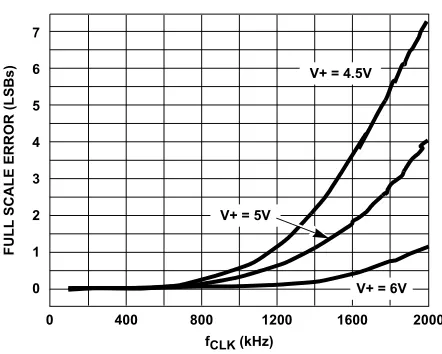
FIGURE 6. FULL SCALE ERROR vs fCLK FIGURE 7. EFFECT OF UNADJUSTED OFFSET ERROR
FIGURE 8. OUTPUT CURRENT vs TEMPERATURE FIGURE 9. POWER SUPPLY CURRENT vs TEMPERATURE
Typical Performance Curves
(Continued)F U L L S C A L E ER R O R (L SB s ) 7 6 5 4 3 2 1 0
fCLK (kHz)
0 400 800 1200 1600 2000
V+ = 4.5V
V+ = 5V
V+ = 6V
VIN(+) = VIN(-) = 0V ASSUMES VOS = 2mV THIS SHOWS THE NEED FOR A ZERO ADJUSTMENT IF THE SPAN IS REDUCED
O F F SE T ER R O R (L SB s ) 16 14 12 10 8 6 4 2
VREF/2 (V) 0
0.01 0.1 1.0 5
O U T PU T C U R R E N T (m A ) 8 7 6 5 4 3 2 -50
TA AMBIENT TEMPERATURE (oC) -ISINK
VOUT = 0.4V
ISOURCE VOUT = 2.4V DATA OUTPUT
BUFFERS
V+ = 5V
-25 0 25 50 75 100 125
PO W E R S U P P L Y C U R R EN T (m A )
TA AMBIENT TEMPERATURE (oC)
-50 -25 0 25 50 75 100 125
1.6 1.5 1.4 1.3 1.2 1.1 1.0
fCLK = 640kHz
V+ = 5.5V
V+ = 5.0V
V+ = 4.5V
Timing Diagrams
FIGURE 10A. START CONVERSION
tWI
tW(WR)I
1 TO 8 x 1/fCLK INTERNAL TC CS
WR
ACTUAL INTERNAL STATUS OF THE CONVERTER
INTR
(LAST DATA READ) (LAST DATA NOT READ)
“NOT BUSY”
“BUSY”
DATA IS VALID IN OUTPUT LATCHES
INTR ASSERTED
tVI 1/2 fCLK
[image:30.612.59.278.301.474.2] [image:30.612.330.557.306.476.2] [image:30.612.89.517.549.700.2]FIGURE 10B. OUTPUT ENABLE AND RESET INTR
Timing Diagrams
(Continued)VALID DATA VALID DATA INTR RESET INTR CS RD DATA OUTPUTS THREE-STATE (HI-Z) tRI tACC
t1H, t0H
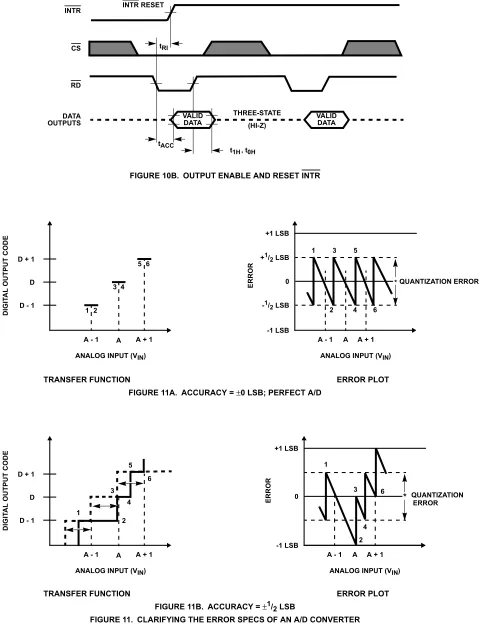
TRANSFER FUNCTION ERROR PLOT
FIGURE 11A. ACCURACY = ±0 LSB; PERFECT A/D
TRANSFER FUNCTION ERROR PLOT
FIGURE 11B. ACCURACY = ±1/2 LSB
FIGURE 11. CLARIFYING THE ERROR SPECS OF AN A/D CONVERTER
ANALOG INPUT (VIN)
D IG IT A L O U T PU T C O D E
D + 1
D
D - 1
A + 1 A A - 1
3 2 1 5 6 4 3 2 1 5 6 4 ER R O R 0 +1 LSB -1 LSB -1/2 LSB +1/2 LSB
* QUANTIZATION ERROR
A
ANALOG INPUT (VIN) A + 1 A - 1
ANALOG INPUT (VIN)
D IG IT A L O U T PU T C O D E
D + 1
D
D - 1
A + 1 A A - 1
3
2 1
5 6
4 0 *
+1 LSB -1 LSB QUANTIZATION ER R O R 3 2 1 6 4
ANALOG INPUT (VIN) A + 1 A A - 1
ERROR
[image:31.612.127.486.86.242.2]Understanding A/D Error Specs
A perfect A/D transfer characteristic (staircase wave-form) is shown in Figure 11A. The horizontal scale is analog input voltage and the particular points labeled are in steps of 1 LSB (19.53mV with 2.5V tied to the VREF/2 pin). The digital output codes which correspond to these inputs are shown as D-1, D, and D+1. For the perfect A/D, not only will center-value (A - 1, A, A + 1, . . .) analog inputs produce the correct output digital codes, but also each riser (the transitions between adjacent output codes) will be located ±1/2 LSB away from each center-value. As shown, the risers are ideal and have no width. Correct digital output codes will be provided for a range of analog input voltages which extend
±1/
2 LSB from the ideal center-values. Each tread (the range of analog input voltage which provides the same digital output code) is therefore 1 LSB wide.
The error curve of Figure 11B shows the worst case transfer function for the ADC080X. Here the specification guarantees that if we apply an analog input equal to the LSB analog voltage center-value, the A/D will produce the correct digital code.
Next to each transfer function is shown the corresponding error plot. Notice that the error includes the quantization uncertainty of the A/D. For example, the error at point 1 of Figure 11A is +1/2LSB because the digital code appeared 1/
2 LSB in advance of the center-value of the tread. The error plots always have a constant negative slope and the abrupt upside steps are always 1 LSB in magnitude, unless the device has missing codes.
Detailed Description
The functional diagram of the ADC080X series of A/D converters operates on the successive approximation principle (see Application Notes AN016 and AN020 for a more detailed description of this principle). Analog switches are closed sequentially by successive-approximation logic until the analog differential input voltage [VlN(+) - VlN(-)] matches a voltage derived from a tapped resistor string across the reference voltage. The most significant bit is tested first and after 8 comparisons (64 clock cycles), an 8-bit binary code (1111 1111 = full scale) is transferred to an output latch.
The normal operation proceeds as follows. On the high-to-low transition of the WR input, the internal SAR latches and the shift-register stages are reset, and the INTR output will be set high. As long as the CS input and WR input remain low, the A/D will remain in a reset state. Conversion will start from 1 to 8 clock periods after at least one of these inputs makes a low-to-high transition. After the requisite number of clock pulses to complete the conversion, the INTR pin will make a high-to-low transition. This can be used to interrupt a processor, or otherwise signal the availability of a new conversion. A RD operation (with CS low) will clear the INTR line high again.
connecting INTR to the WR input with CS = 0. To ensure start-up under all possible conditions, an external WR pulse is required during the first power-up cycle. A conversion-in-process can be interrupted by issuing a second start command.
Digital Operation
The converter is started by having CS and WR simultaneously low. This sets the start flip-flop (F/F) and the resulting “1” level resets the 8-bit shift register, resets the Interrupt (INTR) F/F and inputs a “1” to the D flip-flop, DFF1, which is at the input end of the 8-bit shift register. Internal clock signals then transfer this “1” to the Q output of DFF1. The AND gate, G1, combines this “1” output with a clock signal to provide a reset signal to the start F/F. If the set signal is no longer present (either WR or CS is a “1”), the start F/F is reset and the 8-bit shift register then can have the “1” clocked in, which starts the conversion process. If the set signal were to still be present, this reset pulse would have no effect (both outputs of the start F/F would be at a “1” level) and the 8-bit shift register would continue to be held in the reset mode. This allows for asynchronous or wide CS and WR signals.
After the “1” is clocked through the 8-bit shift register (which completes the SAR operation) it appears as the input to DFF2. As soon as this “1” is output from the shift register, the AND gate, G2, causes the new digital word to transfer to the Three-State output latches. When DFF2 is subsequently clocked, the Q output makes a high-to-low transition which causes the INTR F/F to set. An inverting buffer then supplies the INTR output signal.
When data is to be read, the combination of both CS and RD being low will cause the INTR F/F to be reset and the three-state output latches will be enabled to provide the 8-bit digital outputs.
Digital Control Inputs
The digital control inputs (CS, RD, and WR) meet standard TTL logic voltage levels. These signals are essentially equivalent to the standard A/D Start and Output Enable control signals, and are active low to allow an easy interface to microprocessor control busses. For non-microprocessor based applications, the CS input (pin 1) can be grounded and the standard A/D Start function obtained by an active low pulse at the WR input (pin 3). The Output Enable function is achieved by an active low pulse at the RD input (pin 2).
Analog Operation
successive approximation register. A correction is made to offset the comparison by 1/2 LSB (see Figure 11A).
Analog Differential Voltage Inputs and Common-Mode Rejection
This A/D gains considerable applications flexibility from the analog differential voltage input. The VlN(-) input (pin 7) can be used to automatically subtract a fixed voltage value from the input reading (tare correction). This is also useful in 4mA - 20mA current loop conversion. In addition, common-mode noise can be reduced by use of the differential input.
The time interval between sampling VIN(+) and VlN(-) is 41/2 clock periods. The maximum error voltage due to this slight time difference between the input voltage samples is given by:
where:
∆VE is the error voltage due to sampling delay,
VPEAK is the peak value of the common-mode voltage,
fCM is the common-mode frequency.
For example, with a 60Hz common-mode frequency, fCM, and a 640kHz A/D clock, fCLK, keeping this error to 1/4 LSB (~5mV) would allow a common-mode voltage, VPEAK, given by:
,
or
.
The allowed range of analog input voltage usually places more severe restrictions on input common-mode voltage levels than this.
An analog input voltage with a reduced span and a relatively large zero offset can be easily handled by making use of the differential input (see Reference Voltage Span Adjust).
Analog Input Current
The internal switching action causes displacement currents to flow at the analog inputs. The voltage on the on-chip
capacitance to ground is switched through the analog differential input voltage, resulting in proportional currents entering the VIN(+) input and leaving the VIN(-) input. These current transients occur at the leading edge of the internal clocks. They rapidly decay and do not inherently cause errors as the on-chip comparator is strobed at the end of the clock perIod.
Input Bypass Capacitors
Bypass capacitors at the inputs will average these charges and cause a DC current to flow through the output resistances of the analog signal sources. This charge pumping action is worse for continuous conversions with the VIN(+) input voltage at full scale. For a 640kHz clock frequency with the VIN(+)
input at 5V, this DC current is at a maximum of approximately 5µA. Therefore, bypass capacitors should not be used at the analog inputs or the VREF/2 pin for high resistance sources (>1kΩ). If input bypass capacitors are necessary for noise filtering and high source resistance is desirable to minimize capacitor size, the effects of the voltage drop across this input resistance, due to the average value of the input current, can be compensated by a full scale adjustment while the given source resistor and input bypass capacitor are both in place. This is possible because the average value of the input current is a precise linear function of the differential input voltage at a constant conversion rate.
Input Source Resistance
Large values of source resistance where an input bypass capacitor is not used will not cause errors since the input currents settle out prior to the comparison time. If a low- pass filter is required in the system, use a low-value series resistor (≤1kΩ) for a passive RC section or add an op amp RC active low-pass filter. For low-source-resistance applications (≤1kΩ), a 0.1µF bypass capacitor at the inputs will minimize EMI due to the series lead inductance of a long wire. A 100Ω series resistor can be used to isolate this capacitor (both the R and C are placed outside the feedback loop) from the output of an op amp, if used.
Stray Pickup
The leads to the analog inputs (pins 6 and 7) should be kept as short as possible to minimize stray signal pickup (EMI). Both EMI and undesired digital-clock coupling to these inputs can cause system errors. The source resistance for these inputs should, in general, be kept below 5kΩ. Larger values of source resistance can cause undesired signal pickup. Input bypass capacitors, placed from the analog inputs to ground, will eliminate this pickup but can create analog scale errors as these capacitors will average the transient input switching currents of the A/D (see Analog Input Current). This scale error depends on both a large source resistance and the use of an input bypass capacitor. This error can be compensated by a full scale adjustment of the A/D (see Full Scale
Adjustment) with the source resistance and input bypass capacitor in place, and the desired conversion rate.
Reference Voltage Span Adjust
For maximum application flexibility, these A/Ds have been designed to accommodate a 5V, 2.5V or an adjusted voltage reference. This has been achieved in the design of the IC as shown in Figure 12.
Notice that the reference voltage for the IC is either 1/2 of the voltage which is applied to the V+ supply pin, or is equal to the voltage which is externally forced at the VREF/2 pin. This allows for a pseudo-ratiometric voltage reference using, for the V+ supply, a 5V reference voltage. Alternatively, a voltage less than 2.5V can be applied to the VREF/2 input. The internal gain to the VREF/2 input is 2 to allow this factor of 2 reduction in the reference voltage.
VE(MAX)
∆ (VPEAK)(2πfCM) 4.5
fCLK
---=
VPEAK
∆VE MAX( ) f CLK
( )
2πfCM
( )(4.5)
---=
VPEAK 5 10 3 –
×
( )(640×103)
6.28
( )( )60 (4.5)
---≅1.9V
=
Such an adjusted reference voltage can accommodate a reduced span or dynamic voltage range of the analog input voltage. If the analog input voltage were to range from 0.5V to 3.5V, instead of 0V to 5V, the span would be 3V. With 0.5V applied to the VlN(-) pin to absorb the offset, the reference voltage can be made equal to 1/2 of the 3V span or 1.5V. The A/D now will encode the VlN(+) signal from 0.5V to 3.5V with the 0.5V input corresponding to zero and the 3.5V input corresponding to full scale. The full 8 bits of resolution are therefore applied over this reduced analog input voltage range. The requisite connections are shown in Figure 13. For expanded scale inputs, the circuits of Figures 14 and 15 can be used.
Reference Accuracy Requirements
The converter can be operated in a pseudo-ratiometric mode or an absolute mode. In ratiometric converter applications, the magnitude of the reference voltage is a factor in both the output of the source transducer and the output of the A/D converter and therefore cancels out in the final digital output code. In absolute conversion applicatIons, both the initial value and the temperature stability of the reference voltage are important accuracy factors in the operation of the A/D converter. For VREF/2 voltages of 2.5V nominal value, initial errors of ±10mV will cause conversion errors of ±1 LSB due to the gain of 2 of the VREF/2 input. In reduced span applications, the initial value and the stability of the VREF/2 input voltage become even more important. For example, if the span is reduced to 2.5V, the analog input LSB voltage value is correspondingly reduced from 20mV (5V span) to
10mV and 1 LSB at the VREF/2 input becomes 5mV. As can
be seen, this reduces the allowed initial tolerance of the reference voltage and requires correspondingly less absolute change with temperature variations. Note that spans smaller than 2.5V place even tighter requirements on the initial accuracy and stability of the reference source.
[image:34.612.328.564.52.201.2]In general, the reference voltage will require an initial adjustment. Errors due to an improper value of reference voltage appear as full scale errors in the A/D transfer FIGURE 12. THE VREFERENCE DESIGN ON THE IC
FIGURE 13. OFFSETTING THE ZERO OF THE ADC080X AND PERFORMING AN INPUT RANGE (SPAN) ADJUSTMENT
V+
DGND VREF/2
AGND
(VREF)
R R DIGITAL CIRCUITS ANALOG CIRCUITS 9 8 10 20 DECODE 300
TO VREF/2
TO VIN(-) ZERO SHIFT VOLTAGE
[image:34.612.51.287.226.524.2]0.1µF 5V -+ VREF (5V) FS ADJ. “SPAN”/2 ICL7611
[image:34.612.333.559.238.384.2]FIGURE 14. HANDLING ±10V ANALOG INPUT RANGE
FIGURE 15. HANDLING ±5V ANALOG INPUT RANGE
VIN(-) 2R
5V
2R VIN± 10V
R
VIN(+)
(VREF)
V+ 20
10µF 6 7 + ADC0803-ADC0804 VIN(-) R 5V
VIN±5V
R
VIN(+)
(VREF)
V+ 20
[image:34.612.55.280.561.685.2]function. IC voltage regulators may be used for references if the ambient temperature changes are not excessive.
Zero Error
The zero of the A/D does not require adjustment. If the minimum analog input voltage value, VlN(MlN), is not ground, a zero offset can be done. The converter can be made to output 0000 0000 digital code for this minimum input voltage by biasing the A/D VIN(-) input at this VlN(MlN) value (see Applications section). This utilizes the differential mode operation of the A/D.
The zero error of the A/D converter relates to the location of the first riser of the transfer function and can be measured by grounding the VIN(-) input and applying a small magnitude positive voltage to the VIN(+) input. Zero error is the difference between the actual DC input voltage which is necessary to just cause an output digital code transition from 0000 0000 to 0000 0001 and the ideal 1/2 LSB value (1/2 LSB = 9.8mV for VREF/2 = 2.500V).
Full Scale Adjust
The full scale adjustment can be made by applying a differential input voltage which is 11/2 LSB down from the desired analog full scale voltage range and then adjusting the magnitude of the VREF/2 input (pin 9) for a digital output code which is just changing from 1111 1110 to 1111 1111. When offsetting the zero and using a span-adjusted VREF/2 voltage, the full scale adjustment is made by inputting VMlN to the VIN(-) input of the A/D and applying a voltage to the VIN(+) input which is given by:
,
where:
VMAX = the high end of the analog input range, and
VMIN = the low end (the offset zero) of the analog range. (Both are ground referenced.)
Clocking Option
The clock for the A/D can be derived from an external source such as the CPU clock or an external RC network can be added to provIde self-clocking. The CLK IN (pin 4) makes use of a Schmitt trigger as shown in Figure 16.
Heavy capacitive or DC loading of the CLK R pin should be avoided as this will disturb normal converter operation.
Loads less than 50pF, such as driving up to 7 A/D converter clock inputs from a single CLK R pin of 1 converter, are allowed. For larger clock line loading, a CMOS or low power TTL buffer or PNP input logic should be used to minimize the loading on the CLK R pin (do not use a standard TTL buffer).
Restart During a Conversion
If the A/D is restarted (CS and WR go low and return high) during a conversion, the converter is reset and a new conversion is started. The output data latch is not updated if the conversion in progress is not completed. The data from the previous conversion remain in this latch.
Continuous Conversions
In this application, the CS input is grounded and the WR input is tied to the INTR output. This WR and INTR node should be momentarily forced to logic low following a power-up cycle to insure circuit operation. See Figure 17 for details.
Driving the Data Bus
This CMOS A/D, like MOS microprocessors and memories, will require a bus driver when the total capacitance of the data bus gets large. Other circuItry, which is tied to the data bus, will add to the total capacitive loading, even in three-state (high-impedance mode). Back plane busing also greatly adds to the stray capacitance of the data bus.
There are some alternatives available to the designer to handle this problem. Basically, the capacitive loading of the data bus slows down the response time, even though DC specifications are still met. For systems operating with a relatively slow CPU clock frequency, more time is available in which to establish proper logic levels on the bus and therefore higher capacitive loads can be driven (see Typical Performance Curves).
At higher CPU clock frequencies time can be extended for I/O reads (and/or writes) by inserting wait states (8080) or using clock-extending circuits (6800).
VIN +( )fSADJ VMAX 1.5 (VMAX–VMIN) 256 ---– = CLK R 4 CLK IN CLK ADC0803-ADC0804
fCLK≅ 19
R
C
[image:35.612.325.563.279.452.2]1 1.1 RC R ≅10kΩ
FIGURE 16. SELF-CLOCKING THE A/D
11 12 13 14 15 16 17 18 20 19 10 9 8 7 6 5 4 3 2 1
ADC0803 - ADC0804
WR RD CS
INTR CLK IN
VIN (-) VIN (+)
DGND VREF/2 AGND DB1 DB0 DB4 DB3 DB2 DB7 DB6 DB5 CLK R V+
10K 5V (V
REF)
[image:35.612.72.270.580.690.2]10µF + DATA START ANALOG INPUTS 150pF OUTPUTS N.O. MSB LSB
Finally, if time is short and capacitive loading is high, external bus drivers must be used. These can be three-state buffers (low power Schottky is recommended, such as the 74LS240 series) or special higher-drive-current products which are designed as bus drivers. High-current bipolar bus drivers with PNP inputs are recommended.
Power Supplies
Noise spikes on the V+ supply line can cause conversion errors as the comparator will respond to this noise. A low-inductance tantalum filter capacitor should be used close to the converter V+ pin, and values of 1µF or greater are recommended. If an unregulated voltage is available in the system, a separate 5V voltage regulator for the converter (and other analog circuitry) will greatly reduce digital noise on the V+ supply. An lCL7663 can be used to regulate such a supply from an input as low as 5.2V.
Wiring and Hook-Up Precautions
Standard digital wire-wrap sockets are not satisfactory for breadboarding with this A/D converter. Sockets on PC boards can be used. All logic signal wires and leads should be grouped and kept as far away as possible from the analog signal leads. Exposed leads to the analog inputs can cause undesired digital noise and hum pickup; therefore, shielded leads may be necessary in many applications.
A single-point analog ground should be used which is separate from the logic ground points. The power supply bypass capacitor and the self-clockIng capacitor (if used) should both be returned to digital ground. Any VREF/2 bypass capacitors, analog input filter capacitors, or input signal shielding should be returned to the analog ground point. A test for proper grounding is to measure the zero error of the A/D converter. Zero errors in excess of 1/4 LSB can usually be traced to improper board layout and wiring (see Zero Error for measurement). Further information can be found in Application Note AN018.
Testing the A/D Converter
There are many degrees of complexity associated with testing an A/D converter. One of the simplest tests is to apply a known analog input voltage to the converter and use LEDs to display the resulting digital output code as shown in Figure 18.
For ease of testing, the VREF/2 (pin 9) should be supplied with 2.560V and a V+ supply voltage of 5.12V should be used. This provides an LSB value of 20mV.
If a full scale adjustment is to be made, an analog input voltage of 5.090V (5.120 - 11/2 LSB) should be applied to the VIN(+) pin with the VIN(-) pin grounded. The value of the VREF/2 input voltage should be adjusted until the digital output code is just changing from 1111 1110 to 1111 1111. This value of VREF/2 should then be used for all the tests.
The digital-output LED display can be decoded by dividing the 8 bits into 2 hex characters, one with the 4
most-significant bits (MS) and one with the 4 least-most-significant bits (LS). The output is then interpreted as a sum of fractions times the full scale voltage:
.
For example, for an output LED display of 1011 0110, the MS character is hex B (decimal 11) and the LS character is hex (and decimal) 6, so:
.
Figures 19 and 20 show more sophisticated test circuits.
Typical Applications
Interfacing 8080/85 or Z-80 Microprocessors
VOUT MS 16 --- LS 256 ---+ (5.12)V
=
START
VIN (+)
DGND 2.560V
AGND
10µF 150pF
N.O.
0.1µF 0.1µF
TANTALUM 5.120V
5V
1.3kΩ LEDs (8) (8)
MSB LSB 10kΩ
VREF/2
[image:36.612.322.561.88.297.2]+ 11 12 13 14 15 16 17 18 20 19 10 9 8 7 6 5 4 3 2 1 ADC0803-ADC0804
FIGURE 18. BASIC TESTER FOR THE A/D
VOUT 11 16 --- 6 256 ---+
(5.12) 3.64V
= = ANALOG INPUTS “A” R “B” R R R “C” 100R -+ A2 8-BIT A/D UNDER TEST 10-BIT DAC
VANALOG OUTPUT
100X ANALOG
-+ A1
[image:36.612.327.564.418.544.2]ERROR VOLTAGE
FIGURE 19. A/D TESTER WITH ANALOG ERROR OUTPUT. THIS CIRCUIT CAN BE USED TO GENERATE “ERROR PLOTS” OF FIGURE 11.
A/D UNDER TEST 10-BIT DAC DIGITAL VANALOG INPUTS DIGITAL OUTPUTS