A Novel HDL Coding Style for Power Reduction
in FPGAs
Thomas Marconi, Dimitris Theodoropoulos,
Koen Bertels, Georgi Gaydadjiev
Computer Engineering Lab
Delft University of Technology
{
thomas,dtheodor,koen,georgi
}
@ce.et.tudelft.nl
Technical Report
CE-TR-2010-02
Abstract
1
Introduction
It is well known that dynamic power consumption is linearly proportional to switching activity and capacitance and has a quadratical relation to supply voltage. Therefore, one of the ways to reduce dynamic power consumption is to reduce switching activity. In real systems, many transitions are not necessary. For example, rewriting a register with the same value as its original one, is not needed. This unneeded transition increases switching activity, thus consuming power for doing useless operations. Moreover, as reported in [17], even low-power flip-flops consume low-power during logic transition from zero-to-zero and from one-to-one.
Hardware Description Language (HDL) coding style can affect performance, area and power consumption. We observe that almost all existing coding styles focus on improving performance and reducing area. In our coding style, we focus on reducing power consumption. Another observation is that all existing styles still use what we call it as ”conventional coding style”. In conventional coding style, each flop is coded into one process. This process will generate a D flip-flop (DFF) with the D input coming from the output of the corresponding next state function. Since the clock input of DFF is directly connected to the clock signal, the DFF is always clocked even when it is not necessary. For example,
when the D input has the same logic value as the Q output (D=Q), the DFF
does not need to be clocked. This unnecessary logic transition wastes power. To avoid such unnecessary transitions, a new HDL coding style to reduce power consumption for reconfigurable devices is proposed. The Microelectronic Center of North Carolina (MCNC) benchmark circuits [1] are used to evaluate the proposed coding style compared to conventional coding style. Our proposal can be used with any HDL. In this paper, we illustrate it using VHDL. Each MCNC benchmark circuit is converted into two VHDL files to represent two VHDL coding styles (conventional coding style and our proposal). The VHDL files are implemented in a real FPGA (Stratix EP1S10F484C5 from Altera) using a real existing FPGA tool (Quartus II 6.0 from Altera). The effect of the proposed VHDL coding style on power consumption, area, and performance is evaluated in comparison with conventional one.
The main contributions of this report are:
• a novel low power coding style for reconfigurable devices;
• reduction in total power consumption by 13-90 % with 0-45 % area
over-head;
• performance improvement by 2-20 %.
2
Related work
Coding style when using HDL, like VHDL or Verilog, can affect a lot the design performance, FPGA area utilization and power consumption. For this reason many technical reports and papers provide guides to the users that present
op-timal ways of describing hardware circuits. One of the early references about
how HDL coding style affects design performance is presented in [2]. The author mainly focuses on certain VHDL constructs and how efficiently are interpreted by synthesis tools. A similar work is presented in [3], where a VHDL design methodology adapted to FPGA architectures is described. The authors dis-cuss how different VHDL constructs can lead to suboptimal implementations. Furthermore, they compare different Finite State Machines (FSMs) encoding schemes when mapped onto FPGAs and ASICs. They conclude that one-hot encoding is the fastest and one of the smallest representations for FPGAs, how-ever it is a resource demanding approach for ASICs.
A more recent study focusing on FSMs is presented in [4]. The author de-signed three different FSMs using one, two and three blocks to describe them, under different encoding approaches. The conclusions were that a one-block approach should be avoided, because it is more error prone to coding mistakes. Furthermore, the author suggests to use a two-block approach for FSM designs with combinational outputs and a three-block approach for registered ones. An-other similar study on FSM coding styles for FPGAs is presented in [5]. The authors designed a FSM with three different methods, namely Combined Single Process (CSP), State Separated Combinational Outputs (SCO) and State Sep-arated Registered Outputs (SRO), using one-hot and Grey encoding schemes. Results reported in the paper suggest that the SRO style requires the fewest Look-Up-Tables (LUTs), however a slightly increased number of flip flops, com-paring to the other two styles.
In [6] and [7] Xilinx and Altera provide documents to hardware designers for crafting fast and reliable HDL code respectively. For example, in [6] the authors describe how commonly used modules, like FSMs, counters, clock enables, com-parators and memories, should be inferred to the HDL code in order to avoid performance degradation during synthesis. An even more elaborated document regarding design performance acceleration is presented from the same company in [8]. The authors address many important factors that can help improving the design by increasing the maximum operating frequency and/or reducing area utilization. For example, they present how sub-optimal reset strategies prevent the use of synchronous elements of dedicated hardware blocks or constraint placement and routing due to high reset fanout. Furthermore, they emphasize on how improper HDL coding style, like nestedif-then-else andcase constructs should be avoided, because signal length becomes too long and inhibits opti-mizations from synthesis tools.
Table 1: Related work categorized according to optimization goals
Optimization goal
Reference
Performance
[2], [3], [4], [5], [6], [7], [8], [10]
Area
[2], [3], [4], [5], [6], [7], [8], [9], [10]
Power
[11], [12], [13]
the paper is that following the signal priorities of flip-flops, allows the synthesis tools to optimize designs for low area utilization.
An interesting case study is presented in [10]. The authors describe an ex-periment that was conducted about how HDL coding style affects design perfor-mance. Five hardware engineers with experience ranging from two to seven years implemented the same algorithm in hardware using behavioral and structural HDL style. Designs were mapped onto Xilinx and Altera FPGAs. For design synthesis all engineers used the integrated synthesis tool along with third party synthesis tools. Reported results are very interesting since they demonstrate how in many cases an HDL behavioral approach leads to more efficient imple-mentations comparing to structural descriptions. This fact is also supported by [8], where the authors explicitly suggest to describe designs behaviorally as much as possible.
HDL coding style to reduce power consumption in a literature is clock gating. Clock gating is used to reduce dynamic power consumption by selectively stop the clock signal to go to storage elements when no state or output transition takes place. A circuit with fewer signal transitions consumes less power. It is applied in FPGAs as reported in [11][12][13].
Almost all coding styles focus on improving performance and reducing area as shown in Table 1. In our coding style, we focus on reducing power consump-tion. Our coding style is different from clock gating. In clock gating [11][12][13], the process to represent each flip-flop is modeled by DFF with the D input from the output of the next state function; while in our style, the flip-flop is modeled by T flip-flop (TFF) with the T input at logic one. This is related to the fact that designing sequential circuits using TFFs is more power efficient than DFFs as already reported in [16]. Moreover, there is no next state function anymore that goes to the input of T flip-flop; the input of T flip-flop is constant at logic one. To know when to stop clock signal, the clock gating needs a controller that has a knowledge of the circuit behavior. In our style, the controller has been unified with the next state function circuit.
3
Proposed HDL coding style
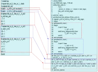
flip-Figure 1: An example of blif file to conventional VHDL file conversion (lion.blif to lion conv.vhd)
flops (lines 4 and 5) and three combinational logic functions (lines 6-8). Line 6 is the output function; while lines 7 and 8 are next state functions. In conventional coding style, each flip-flop is coded into one process as shown in the right side of Figure 1. This process will generate a D flip-flop (DFF) with the D input from the output of corresponding next state function (NSF) as shown in Figure 2. In this circuit, the output of each NSF is connected to the D input of DFF. When the D input of DFF (in this figure, for example: n n10 and n n11) has
a different value compared to its Q output (D ̸= Q), the DFF needs to be
clocked for updating the storage data (in this figure, for example: n n21 and n n22). Otherwise, when the D input has the same logic value as the Q output (D=Q), the DFF does not need to be clocked. However, since the clock input of DFF is directly connected to the clock signal, the DFF is always clocked. This unnecessary logic transition wastes power in this generated circuit using conventional style.
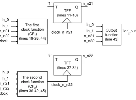
Output function (line 28) In_0
In_1 n_n21 n_n22
lion_out The first
next state Function
(NSF1)
(line 29)
DFF (lines 12-19) In_0
In_1 n_n21 n_n22
D Q n_n21
clock
The second next state
Function (NSF2)
(line 30)
DFF (lines 20-27) In_0
In_1 n_n21 n_n22
D Q
n_n11 n_n22
clock
n_n10
Figure 2: An example of implemented circuit for the lion benchmark using conventional coding style
The second
Figure 4: An example of implemented circuit for the lion benchmark using our coding style
function (CF) as shown in an example of implemented circuit in Figure 4. The TFF is clocked when it is needed to update storage data (in this simple example: n n21 and n n22); otherwise, it will not be clocked. In this simple circuit, for example if present state of n n21 is different from next state of n n21, the TFF will be clocked by clock n n21; otherwise, it will not be clocked to save power.
Avoiding unnecessary clock transitions is one of benefits of this new coding style compared to conventional coding style. Each combinational circuit stops clock signal to be propagated to an individual FF when the state of the FF does not change. As a result, the unnecessary clock transitions are totally avoided. In comparison to clock gating, our coding style does not need an additional clock gating controller. Therefore, additional power and area are also saved in comparison to clock gating approach.
Moreover, circuits generated using our proposed coding style can run faster than circuits using conventional coding style. This can be explained as follows. In conventional circuits, the DFF can be clocked properly if its D input is stable at least before its setup time (tsetup(DF F)). In our circuits, since the T input of the TFF is always in logic one, the TFF is always ready to be clocked. As a result, logic circuits implemented using our style can be clocked faster than logic circuits using conventional style. In this simple example, we can obtain the clock period of the circuit using conventional style asTc(Conv)≥ M ax(tpd(N SF1),
In our style, we need to feed clock signal to combinational circuits (imple-mented in LUTs in FPGAs) before it goes to flip-flops. This can be easily applied since not all inputs of LUTs are utilized in real FPGA designs as re-ported in [15]. Therefore, we can use these unused inputs to feed clock signal for free in FPGAs.
If the input of circuit changes during clock signal at logic one, there is a chance that this input generates a pulse that can affect the state of TFF. The first solution of this problem is to use the pulsed clock signal. The width of pulsed clock signal is set to be the minimum pulsed clock width of TFF. Since the width of the pulsed clock signal is so narrow, the possibility that inputs change during this very short period is kept low. If it occurs, the width of the pulse caused by this condition is always less than the width of the original pulsed clock signal. Since the width of this pulse is smaller than the minimum pulsed clock width of TFF, the pulse is ignored; the state of TFFs will not be affected. As a result, the circuit will keep working properly. The second solution for this clocking problem is to synchronize the input with clock signal before it goes to the actual circuit. Since inputs are synchronized, the changing of input during clock at logic one will be ignored by the circuit. However, this requires additional logic, latency and power. In this work, we performed experiments using a pulsed clock solution.
4
Evaluation
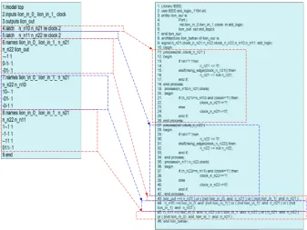
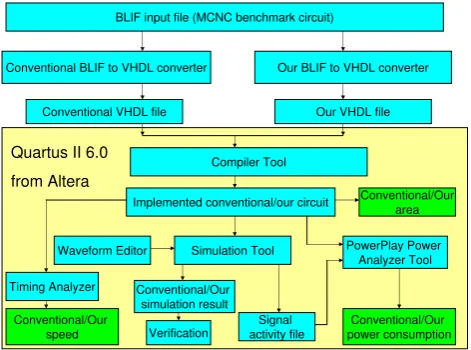
The experimental setup is shown in Figure 5. Each MCNC benchmark circuit [1] is converted into two VHDL files (conventional and our VHDL files) to represent the two VHDL coding styles (conventional and our coding styles). An example of blif file to conventional VHDL file conversion is presented in Figure 1; while an example of blif file to our VHDL file conversion is presented in Figure 3.
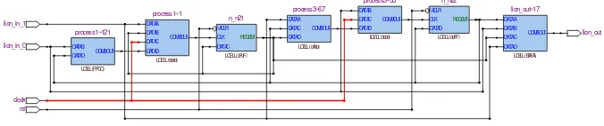
Each VHDL file is compiled for Stratix EP1S10F484C5 using Compiler Tool from Quartus II. An example of implemented circuit for conventional VHDL style is presented in Figure 6(a). It can be shown in this figure that all flip-flops of implemented circuit using conventional VHDL style are directly connected to clock signal. Figure 6(b) shows the same circuit implemented using our VHDL style. Each flip-flop is not directly connected to the clock signal. The flip-flop is only clocked if needed. The area needed for implementing each circuit in the number of logic elements (LEs) is reported by Compiler Tool. In this simple example in Figure 6, each circuit (conventional or our circuit) occupies 7 LEs. The TFF is implemented using the LE with its registered output connected to its input data.
BLIF input file (MCNC benchmark circuit)
Conventional BLIF to VHDL converter
Conventional VHDL file
Compiler Tool
Implemented conventional/our circuit Conventional/Ourarea
Simulation Tool
Our BLIF to VHDL converter
Our VHDL file
Figure 5: Experimental setup
Besides generating simulation results, the Simulation Tool also generates the signal activity file (SAF). To evaluate power consumption, this SAF file and the implemented circuit from the previous step are fed into the PowerPlay Power Analyzer Tool from Quartus II to obtain total power, dynamic power, and static power.
To compare the performances of the implemented circuits, Timing Analyzer from Quartus II is used. The performance is obtained in terms of maximum clock frequency.
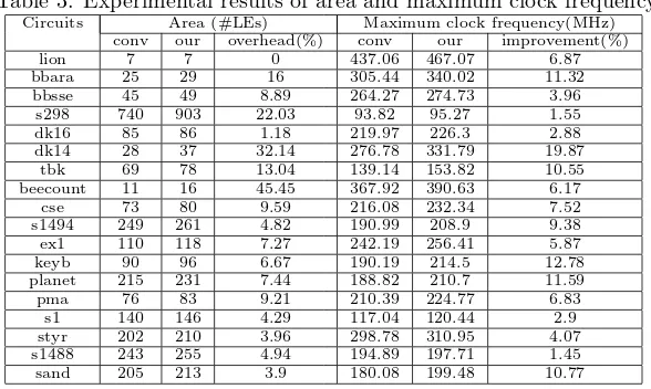
The experimental results using a 50 MHz clock are presented in Table 2. This table shows that our VHDL style can lead to reduction in dynamic power and total power, but it cannot reduce static power. Since our VHDL style can avoid unnecessary transitions by clocking flip-flops only if needed, our VHDL style can lead to reduction in dynamic power consumption (75 % on average) compared to conventional VHDL style. The degree of power reduction depends on the nature of the circuit, circuits with many unnecessary transitions can take more advantages of our style in terms of power consumption. This 75 % dynamic power reduction can only produce 15 % reduction in total power consumption on average at 50 MHz since the static power is a dominant power in these circuits at this frequency. If the dominant power is dynamic power, this 75 % reduction in dynamic power will lead to reduction in total power up to 75 %.
(a) Implemented conventional circuit for lion_conv.vhd using Quartus II 6.0
(b) Implemented our circuit for lion_our.vhd using Quartus II 6.0 !ACLR
Figure 6: An example of implemented circuit for lion benchmark circuit using Quartus II
Table 2: Experimental results of power consumption at 50 MHz
Table 3: Experimental results of area and maximum clock frequency
Circuits Area (#LEs) Maximum clock frequency(MHz) conv our overhead(%) conv our improvement(%) lion 7 7 0 437.06 467.07 6.87 bbara 25 29 16 305.44 340.02 11.32 bbsse 45 49 8.89 264.27 274.73 3.96
s298 740 903 22.03 93.82 95.27 1.55 dk16 85 86 1.18 219.97 226.3 2.88 dk14 28 37 32.14 276.78 331.79 19.87
tbk 69 78 13.04 139.14 153.82 10.55 beecount 11 16 45.45 367.92 390.63 6.17
cse 73 80 9.59 216.08 232.34 7.52 s1494 249 261 4.82 190.99 208.9 9.38 ex1 110 118 7.27 242.19 256.41 5.87 keyb 90 96 6.67 190.19 214.5 12.78 planet 215 231 7.44 188.82 210.7 11.59 pma 76 83 9.21 210.39 224.77 6.83
s1 140 146 4.29 117.04 120.44 2.9 styr 202 210 3.96 298.78 310.95 4.07 s1488 243 255 4.94 194.89 197.71 1.45 sand 205 213 3.9 180.08 199.48 10.77
time is becoming far less significant compared to total longest path for more logic level circuits, more logic level leads to less performance improvement.
Since clock signal needs to be fed to LUTs before it goes to flip-flops, our style suffers 0-45% (11 % on average) more area compared to the conventional one, depending on the circuit logic functions. If the clock signal can be fed to LUTs using unused inputs, our style does not need additional LUTs for this purpose. As a result, it will produce lower area overhead or even no area overhead as shown in Table 2. In our experiment, we had considered this area overhead when we evaluated power consumption and performance.
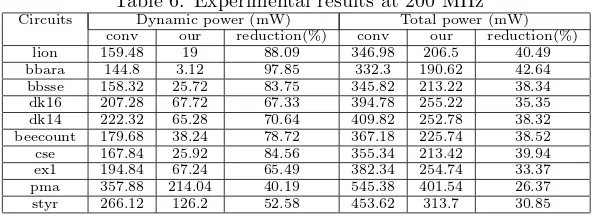
To investigate all implemented circuits further, we run them using different clock frequencies: 100 MHz, 150 MHz, and 200 MHz. The results of this experi-ment are presented in tables 4-6. Since static power, area, and performance are not affected by changing the clock frequency, these tables only show dynamic power and total power consumptions. From these tables, we can see that dy-namic power consumption is linearly proportional with clock frequency. These tables also show that our coding style can reduce total power consumptions by 25 %, 32 %, and 36 % on average compared to conventional style at 100 MHz, 150 Mhz, and 200 MHz, respectively. Since dynamic power is higher when the clock frequency is increased, the reduction of total power is also increased for higher clock frequency.
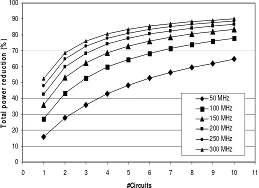
This figure indicates that our coding style can reduce total power by 16-65 % at 50 MHz. Total power is even much more reduced at higher frequency, up to 90 % at 300 MHz. Total power reduction saturates up to its ability to reduce dynamic power as shown in Figure 7.
0
Figure 7: Effect of the number of circuits (#Circuits) on total power reduction (%)
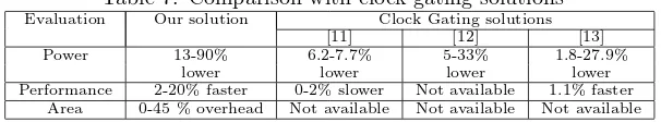
Table 7 shows the comparison between our solution and clock gating solu-tions [11], [12], and [13]. Clock gating solusolu-tions are obtained from the results of the original papers: [11], [12], and [13]. Unlike clock gating, our proposal does not need an additional controller to stop clock propagation. As a result, it saves more power than clock gating solutions. Moreover, since flip-flops are always ready to be clocked in our proposal, it generates faster designs than clock gating designs. The area cannot be directly compared due to no information regarding area overhead in clock gating papers.
5
Conclusions
Table 4: Experimental results at 100 MHz
Circuits Dynamic power (mW) Total power (mW) conv our reduction(%) conv our reduction(%) lion 79.74 9.5 88.09 267.24 197 26.28 bbara 72.4 1.56 97.85 259.9 189.06 27.26 bbsse 79.16 12.86 83.75 266.66 200.36 24.86 dk16 103.64 33.86 67.33 291.14 221.36 23.97 dk14 111.16 32.64 70.64 298.66 220.14 26.29 tbk 80.94 8.6 89.37 268.44 196.1 26.95 beecount 89.84 19.12 78.72 277.34 206.62 25.5
cse 83.92 12.96 84.56 271.42 200.46 26.14 s1494 143.46 54.34 62.12 330.96 241.84 26.93 ex1 97.42 33.62 65.49 284.92 221.12 22.39 keyb 82.18 10.42 87.32 269.68 197.92 26.61 planet 84.66 11.76 86.11 272.16 199.26 26.79 pma 178.94 107.02 40.19 366.44 294.52 19.63 s1 105.9 42.46 59.91 293.4 229.96 21.62 styr 133.06 63.1 52.58 320.56 250.6 21.82 s1488 127.92 60.74 52.52 315.42 248.24 21.3
sand 72.28 0.98 98.64 259.78 188.48 27.45
Table 5: Experimental results at 150 MHz
Circuits Dynamic power (mW) Total power (mW) conv our reduction(%) conv our reduction(%) lion 119.61 14.25 88.09 307.11 201.75 34.31 bbara 108.6 2.34 97.85 296.1 189.84 35.89 bbsse 118.74 19.29 83.75 306.24 206.79 32.47 dk16 155.46 50.79 67.33 342.96 238.29 30.52 dk14 166.74 48.96 70.64 354.24 236.46 33.25 beecount 134.76 28.68 78.72 322.26 216.18 32.92 cse 125.88 19.44 84.56 313.38 206.94 33.97 s1494 215.19 81.51 62.12 402.69 269.01 33.2
ex1 146.13 50.43 65.49 333.63 237.93 28.68 keyb 123.27 15.63 87.32 310.77 203.13 34.64 planet 126.99 17.64 86.11 314.49 205.14 34.77 pma 268.41 160.53 40.19 455.91 348.03 23.66 styr 199.59 94.65 52.58 387.09 282.15 27.11 s1488 191.88 91.11 52.52 379.38 278.61 26.56 sand 108.42 1.47 98.64 295.92 188.97 36.14
Table 6: Experimental results at 200 MHz
creates circuits with 0-45 % more area.
Table 7: Comparison with clock gating solutions
Evaluation Our solution Clock Gating solutions
[11] [12] [13]
Power 13-90% 6.2-7.7% 5-33% 1.8-27.9%
lower lower lower lower
Performance 2-20% faster 0-2% slower Not available 1.1% faster Area 0-45 % overhead Not available Not available Not available
This result motivated new proposal for a low power LE to support this way of implementing circuits as reported in [18]. Instead of using DFFs, we use TFFs with the T input permanently connected to logic one value. Instead of connecting the output of the LUT to the input of the FF, we connect it to the clock input of the FF. The coding style in this paper is a way for us to ”force” the existing CAD tools using the existing FPGAs to implement circuits in a different way than the conventional one. In the future, this new way of implementing circuits could be integrated in the CAD tools.
Acknowledgment
This work is sponsored by the hArtes project (IST-035143) supported by the Sixth Framework Programme of the European Community under the thematic area ”Embedded Systems”.
References
[1] S. Yang, ”Logic Synthesis and Optimization Benchmarks User Guide Ver-sion 3.0,” Tech. Rep., Microelectronic Center of North Carolina, 1991.
[2] S. Samhouri, ”HDL Coding Style for LUT Based FPGAs,” Proceedings of IEEE International Verilog HDL Conference and VHDL International Users Forum, pp. 1-11, 1996.
[3] M. Gschwind and V. Salapura, ”A VHDL Design Methodology for FPGAs,” Proceedings of International Conference on Field Programmable Logic and Applications(FPL), pp. 208-217, 1995.
[4] C. E. Cummings, ”The Fundamentals of Efficient Synthesizable Finite State Machine Design using NC-Verilog and BuildGates,” Proceedings of Inter-national Cadence Usergroup Conference, pp. 1-27, 2002.
[5] N. I. Rafla and B. L. Davisy, ”A Study of Finite State Machine Coding Styles for Implementation in FPGAs,” Proceedings of International Mid-west Symposium on Circuits and Systems, pp. 337-341, 2006.
[7] Altera, ”Quartus II Handbook Version 9.1,” Altera, Tech. Rep., November 2009.
[8] P. Garrault and B. Phiofsky, ”HDL Coding Practices to Accelerate Design Performance,” Xilinx Corporation , Tech. Rep., January 2006.
[9] K. Chapman, ”Get Your Priorities Right – Make Your Design up to 50% smaller,” Xilinx Corporation, Tech. Rep., October 2007.
[10] A. Dollas, K. Papademetriou, E. Sotiriades, D. Theodoropoulos, I. Koidis, and G. Vernardos, ”A Case Study on Rapid Prototyping of Hardware Sys-tems: the Effect of CAD Tool Capabilities, Design Flows, and Design Styles,” Proceedings of IEEE International Workshop on Rapid System Prototyping, pp. 180-186, June 2004.
[11] S. Huda, M. Mallick, J.H. Anderson, ”Clock Gating Architectures for FPGA Power Reduction,” Proceedings of International Conference on Field-Programmable Logic and Applications(FPL), pp. 112-118, 2009.
[12] Y. Zhang, J. Roivainen, A. M¨ammel¨a, ”Clock-Gating in FPGAs: A Novel
and Comparative Evaluation,” Proceedings of EUROMICRO Conference on Digital System Design, pp.584-590, 2006
[13] Q. Wang, S. Gupta, J.H. Anderson, ”Clock Power Reduction for Virtex-5 FPGAs,” Proceedings of International Conference on Field Programmable Gate Arrays (FPGA), pp. 13-22, 2009.
[14] ”Berkeley Logic Interchange Format (BLIF),” University of California Berkeley, February 2005.
[15] S. Mondal and S. O. Memik, ”Fine-grain Leakage Optimization in SRAM based FPGAs,” Proceedings of the ACM Great Lakes Symposium on VLSI, pp. 238-243, 2005.
[16] X. Wu, M. Pedram, ”Low-power Sequential Circuit Design Using T Flip-flops,” International Journal of Electronics, Vol. 88, No. 6, pp. 635-643, June 2001.
[17] D. Markovic, B. Nikolic, R. Brodersen, ”Analysis and Design of Low-energy Flip-flops,” Proceedings of International Symposium on Low Power Elec-tronics and Design, pp.52-55, August 2001.