Effect of substrate temperature on quality of copper film
catalyst substrate: A Molecular Dynamics Study
Rinaldo Marimpul*
Department of Physics, Faculty of Science and Technology, Buddhi Dharma University Jl Imam Bonjol No 41 Tangerang, Indonesia
*Correspondence: [email protected]
A B S T R A C T S A R T I C L E I N F O
Copper film growth using thermal evaporation methods was studied using molecular dynamics simulations. The AlSiMgCuFe modified embedded atom method potential was used to describe interaction of Cu-Cu, Si-Si and Cu-Si atoms. Our results showed that the variations of substrate temperature affected crystal structure composition and surface roughness of the produced copper film catalyst substrate. In this study, we observed intermixing phenomenon after deposition process. The increasing of substrate temperature affected the increasing of the total silicon atoms had diffusion into copper film.
© 2017 Tim Pengembang Journal UPI
Article History: Received 17 Jun 2017 Revised 31 Jul 2017 Accepted 29 Aug 2017 Available online 01 Sep 2017 ____________________ Keyword:
Molecul dynamics simulation, Thermal evaporation method, Substrate temperature, Crystal structure, Surface roughness, Intermixing phenomenon.
Rinaldo Marimpul. Effect of substrate temperature on quality of copper film catalyst sub.. | 184
DOI: http://dx.doi.org/10.17509/ijost.v1i2
1. INTRODUCTION
Copper film has many applications such as ohmic contact and catalyst substrate as medium of graphene growth (Yamada et al., 2012; Bae et al., 2010; Butler et al., 2013). One of criteria of catalyst substrate for graphene growth medium is good crystalinity (Kim et al., 2012). Kim reported that crystalinity of metal catalyst substrate affected physical properties of the produced graphene (Kim et al., 2012).
Many methods of thin film growth were used such as evaporation thermal and sputtering. Sputtering method uses high energy atom on deposition process. Meanwhile, thermal evaporation method uses relatively low energy atom. Therefore, evaporation thermal method tend to produce film with poor quality (amorphous structure). For solving this problem, annealing process is done to repair the structure of film (Rosikhin et al., 2016).
A molecular dynamics simulation study of growth process and annealing of copper film was done by many researchers (Marimpul et al., 2017; Zhang, 2012; Zhang, 2013; Syuhada, 2016; Hidayat et al., 2016). This study is done to get spesific understanding on atomic scale, to predict and to complete experiment result. Marimpul reported that the improvement of film crystalinity at annealing process was initiated by atomic diffusion (Marimpul et al., 2017). Zhang et al. reported that substrate
temperature affected the percentage of crystal structure and surface morphology of film (Zhang, 2012; Zhang, 2013; Syuhada, 2016; Hidayat, 2016).
In this paper, we simulated growth process of copper film on silicon substrate based on thermal evaporation method to get metal catalyst substrate for medium of graphene growth. This study is improvement from previous study (Hidayat, 2016). In
previous work, the simulated study of growth process was based on general deposition and just analyzed effect of substrate temperature on percentage of amorphous structure. We simulated growth process based on thermal evaporation method and modified simulation method. We investigated the effect of substrate temperature on crystal structure and surface morphology of copper film catalyst substrate. We observed the intermixing phenomenon on atomic scale and thus the produced of copper film catalyst substrate can be used for application ohmic contact, besides graphene growth medium.
2. SIMULATION METHOD
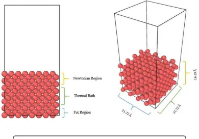
Figure 1 shows the silicon substrate
system with dimensions 4a x 4a x 3a (a = 5.43 Å, the lattice constant of a diamond structure) and consisting of 416 atoms. Periodic boundary conditions were applied in the x and y directions.
There are three regions on silicon substrate, namely fixed region, thermal region and newtonian region. Fixed region consists of three layers of atom who prevent atom moving and fix in position when deposition process. Thermal region consists of six layers of atoms who control substrate temperature to remain constant. Newtonian region consists of four layers of atoms. The motion of atoms in thermal region and
e to ia regio is go er ed y Ne to ’s
equation. For solving the equation of motion,
e used Verlet Algorith ith ti estep ∆t=1
fs. We used Berendsen thermostat to control temperature with a damping parameter of 10 timesteps.
In this process , each copper atom was deposited on silicon substrate every 2000 timesteps. Therefore, deposition rate, in this simulation, is 1 atom/2 ps (Hou et al., 2000). This proceeded until 390 atoms were deposited on the substrate and then system was equilibrated at each temperature 300 K, 400 K, 500 K and 600 K for 1 ns. It was intended to make system in relax condition. All of our simulations were performed using LAMMPS (Large-scale atomic/molecular massively parallel simulator) (Plimpton, 1995). The visualization of system from LAMMPS output data was used by OVITO (Open visualization tool) (Stukowski, 2010). We used common neighbour analysis (CNA) method with OVITO software to calculate and to analyze crystal structure and to calculate surface roughness of catalyst substrate.
The interactions between Si-Si, Cu-Cu and Cu-Si are described by the AlSiMgCuFe modified embedded atom method (MEAM) potential (Jelinek et al., 2012). These interactions are governed by the equation:
= � + ∑ � (� )≠ (1)
where F_i is the electron density function and
ϕ_ij is the interaction of a pair of atoms, limited by a certain cut-off radius. The parameters of the potential interaction function are given in Table 1.
3. RESULTS AND DISCUSSION
3.1. Crystalline structure
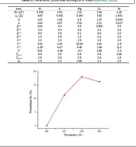
In this simulation, we deposited copper film on silicon substrate. Therefore, the result is copper film catalyst substrate with the expectation of structure crystal was fcc (face centered cubic). Figure 2 shows graphic
of percentage of fcc structure at variation of substrate temperature. From Figure 2 was
shown that the increasing of percentage of fcc structure was occured with the increasing of substrate temperature. The increasing of percentage of crystal structure indicated that film had more neat arrangement of atoms. It was occured because the increasing of substrate temperature affected copper atom gained more thermal energy to overcome barrier energy from the surrounding atoms.
Rinaldo Marimpul. Effect of substrate temperature on quality of copper film catalyst sub.. | 186
DOI: http://dx.doi.org/10.17509/ijost.v1i2
elem. Al Si Mg Cu Fe
� �� 3.353 4.63 1.51 3.54 4.28
� (Å) 4.05 5.431 3.194 3.62 2.851
� 1.07 1.00 0.8 1.07 0.555
4.64 4.87 5.52 5.11 5.027
2.04 4.4 4.0 3.634 3.5
3.0 5.5 3.0 2.2 2.0
6.0 5.5 0.2 6.0 1.0
1.5 5.5 1.2 2.2 1.0
� 1.0 1.0 1.0 1.0 1.0
� 4.50 2.05 10.04 4.91 -1.6
� -2.30 4.47 9.49 2.49 12.5
� 8.01 -1.80 -4.3 2.95 -1.4
0.8 2.0 0.8 0.8 0.68
�� 2.8 2.8 2.8 2.8 1.9
� 1.0 2.2 0.63 1.1 1.0
Thus, copper atom had diffusion on substrate surface and had diffusion toward other copper atoms to form the crystal structure. This result was agreed with Arhennius Law.
The increases in percentage of FCC structure indicated that there was an improvement of crystalinity on copper film catalyst substrate. This result was expected because good crystalinity is one of criteria of catalyst substrate for graphene growth medium. Furthernore, quality of crystalinity of catalyst substrate will affect physical
properties and quality of the produced graphene (Kim et al., 2012).
The interesting phenomenon was a decreased of percentage of fcc structure, from 500 to 600 K. In this condition, the total percentage of crystal structure was increased. However, copper atoms not only formed fcc structure, but also hcp and bcc structure at 600 K as shown in Table 1. Tabel 1. Parameter potensial AlSiMgCuFe meam (Jelinek, 2012)
Substrate temperature
(K)
Percentage of crystal structure (%)
fcc hcp bcc amorf
300 (1/806) x 100 = 0,1 0 0 (805/806) x 100 = 99,9
400 (92/806) x 100 = 11,4 (47/806) x 100 = 5,8 (1/806) x 100 = 0,1 (666/806) x 100 = 82,6
500 (146/806) x 100 = 18,1 0 0 (660/806) x 100 = 81,9
600 (131/806) x 100 = 16,3 (22/806) x 100 = 2,7 (1/806) x 100 = 0,1 (652/806) x 100 = 80,9
3.2. Surface morphology
Surface morphology is one of criteria that related to quality of film. In here, we analyzed effect of substrate temperature to surface roughness of catalyst substrate. Surface morphology affected electrical conductivity of copper film (Timoshevskii, 2008). Timoshevskii reported that surface roughness (1-3 atoms) can decrease 30 – 40 % electrical conductance of copper film. In this study, surface roughness of copper film catalyst substrate was measured quan-titatively using equation of
root-mean-square roughness with OVITO (Stukowski, 2010; Zhang, 2012):
��= √∑ ��−�̅
�
�= (2)
where z_i represents the height of the exposed atoms on catalyst substrate surface.
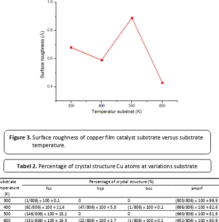
Figure 3 shows that the surface roughness
decreased as the increasing of substrate temperature, as we observed at 400 K and 600 K. This result was agreed with Zhang and Syuhada (Zhang, 2013; Syuhada, 2016).
Figure 3. Surface roughness of copper film catalyst substrate versus substrate
temperature.
Rinaldo Marimpul. Effect of substrate temperature on quality of copper film catalyst sub.. | 188
DOI: http://dx.doi.org/10.17509/ijost.v1i2
The phenomenon of Cu atom diffusion on substrate, in this study, was agreed with
Fi k’s La that stated there as a
dependence of temperature on diffusion coefficient as shown in equation:
= . ��� − �� (3)
where Q_d is activation energy and T is temperature. From this equation, we can see an empirical relationship that temperature is proportional to diffusion coefficient. The increasing of temperatur affected the increasing of diffusion coefficient for D_0 and Q_d were constant. Therefore the surface of copper film catalyst substrate became smoother. However, the interesting phenomenon was occured at 500 K. The increasing of surface roughness, in this condition, opposed with the results at 400 K
and 600 K. This was occured because catalyst substrate at 500 K had only fcc structure. Meanwhile, the composition of crystal structure of catalyst substrate at 400 K and 600 K consists of fcc, hcp and bcc. The difference of this composition affected the arrangement of atoms became not uniform (homogeneous) and thus affected catalyst substrate surface.
3.3. Intermixing phenomenon
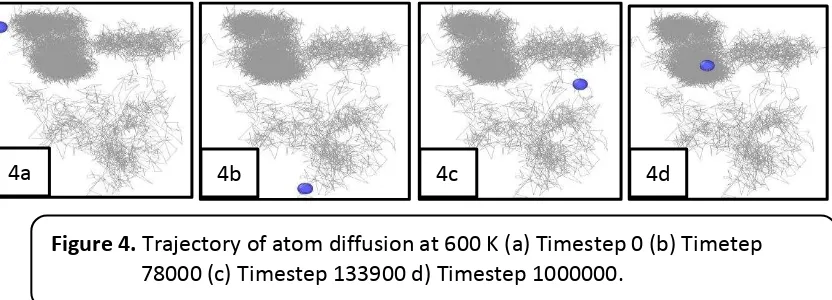
In this study, we also observed intermixing phenomenon. Figure 5 shows intermixing phenomenon on copper film catalyst substrate after deposition process.
Figure 5 shows that Cu (blue colour) and
Si atoms (red colour) at the interface. We also can see copper atom had diffusion to
Figure 4. Trajectory of atom diffusion at 600 K (a) Timestep 0 (b) Timetep
78000 (c) Timestep 133900 d) Timestep 1000000.
Figure 5. Intermixing phenomenon of Cu and Si atoms.
silicon substrate region. This phenomenon was observed by Echigoya. Echigoya reported that the forming amorphous of copper silicide, Cu3Si and Cu15Si4, was caused by the reaction of copper and silicon at interface (Echigoya et al., 1993). The forming of amorphous layer of copper silicide, Cu3Si and Cu15Si4, was expected for application of microelectronic device and ohmic contact.
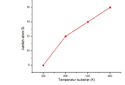
Our results also indicated that there was silicon atoms had diffusion into deposited copper film. Likewise copper atoms had diffusion to silicon substrate region. Figure 6
shows the increasing of substrate temperature affected the increasing of the total of Si atoms had diffusion into deposited copper film. This results lead to the forming of copper silicide (Echigoya et al,. 1993).
4. CONCLUSION
Study of molecular dynamics simulations variation of substrate temperature on growth process of copper film on silicon substrate concluded that:
Parameter of substrate temperature affected the composition of crystal structure. The produced of copper film catalyst substrate at 500 K generated the highest percentage of fcc structure.
The compositions of crystal structure affected surface roughness of copper film catalyst substrate.
5. ACKNOWLEDGEMENTS
Author gratefully acknowledged to Prof. Toto Winata (Department of Physics, Institut Teknologi Bandung) and Dr. Gregoria Illya (Department of Electrical Engineering, Buddhi Dharma University) for valuable comments and discussions.
6. AUTHORS’ NOTE
The author(s) declare(s) that there is no conflict of interest regarding the publication of this article. Authors confirmed that the data and the paper are free of plagiarism.
8. REFERENCES
Bae, S., Kim, H., Lee, Y., Iijima, S.,. (2010). Roll-to-roll production 0f 30-inch graphene films for transparent electrodes. Nature Nanotechnology,5, 574-578.
Butler, S. Z., Hollen, S. M., Cao, L., Goldberger J. E. (2013). Progress, challenges and opportunities in two-dimensional material beyond graphene. ACS Nano, 7, 2898-2926. Figure 6. Number of Si atoms had diffusion into deposited copper film versus
Rinaldo Marimpul. Effect of substrate temperature on quality of copper film catalyst sub.. | 190 Echigoya, J., Satoh, T., Ohmi, T. (1993). Thin film reaction and interface structure of Cu on
(111) Si. Acta Metallurgica et Materialia, 41, 229-234.
Hidayat, A. F., Rosikhin A., Syuhada, I., Winata, T. (2016). Effect of temperature on Cu structure deposited on Si substrate: A molecular dynamics study. AIP Conference Proceedings, 1710 (1), 030039.
Hou, Q., Hou M., Bardotti, L., Prevel, B., Melinon, P., Perez, A. (2000). Deposition of Au N clusters on Au (111) surfaces: I. Atomic-scale modelling. Physical Review B, 62,
2825-2834.
Jelinek, B., Groh, S., Horstemeyer, M. F., Houze, J., Kim, S. G., Wagner, G. J., Moitra, A., Baskes, M. I. (2012). Modified embedded atom method potential for Al, Si, Mg, Cu and Fe alloys. Physical Review B, 85, 1-17.
Kim, K., Artyukhov, V. I., Regan, W., Liu, Y., Crommie M. F., Yakobson, B. I., Zettl, A. (2012). Ripping graphene: preferred directions. Nano Letters, 12, 293-297.
Marimpul, R., Syuhada, I., Rosikhin, A., Winata, T. (2017). Effect of copper film catalyst substrate thickness on atomic diffusion time as the initiation of the recrystallization stage: a molecular dynamics study. Material Research Express, 4 (3), 034004.
Plimpton, S. (1995). Fast parallel algorithms for short-range molecular dynamics. Journal of Computational Physics, 117, 1-19.
Rosikhin, A., Hidayat, A. F., Marimpul, R., Syuhada, I., Winata, T. (2016). Low pressure hand made PVD system for high crystalline metal thin film preparation in micro-nanometer scale. AIP Conference Proceedings, 1710 (1), 030026.
Stukowski, A. (2010). Visualization and analysis of atomistic simulation data with OVITO-the open visualization tool. Modelling and Simulation in Materials and Engineering, 18,
015012.
Syuhada, I., Rosikhin, A., Hidayat, A. F., Noor, F. A., Winata, T. (2016). Molecular dynamics simulation of graphene growth at initial stage on Ni (100) facet for low flux C energy by CVD. AIP Conference Proceedings, 1710 (1), 030060.
Timoshevskii, V., Ke, Y., Guo, H., Gall, D. (2008). The influence of surface roughness on electrical conductance of thin Cu films: an ab initio study. Journal of Applied Physics,
103, 1-4.
Yamada, T., Ishihara, M., Kim, J., Hasegawa, M., Iijima S. (2012). A roll-to-roll microwave plasma chemical vapor deposition process for the production of 294 mm width graphene films at low temperature. Carbon, 50, 2615-2619.
Zhang, J., Liu, C., Fan, J. (2013). Comparison of Cu thin films deposited on Si substrates with different surfaces and temperatures. Applied Surface Science, 276, 417-423.
Zhang, J., Liu, C., Shu, Y., Fan, J. (2012). Growth and properties of Cu thin film deposited on Si (001) substrate: a molecular dynamics simulation study. Applied Surface Science, 261,