ASIC AND FPGA VERIFICATION:
Richard Munden has been using and managing CAE systems since 1987. He has been concerned with simulation and modeling issues for as long.
Richard co-founded the Free Model Foundry (http://eda.org/fmf/)in 1995 and is its president and CEO. He has a day job as CAE/PCB manager at Siemens Ultrasound (previously Acuson Corp) in Mountain View, California. Prior to joining Acuson, he was a CAE manager at TRW in Redondo Beach, California. He is a well-known con-tributor to several EDA users groups and industry conferences.
ASIC AND FPGA
VERIFICATION:
A GUIDE TO
COMPONENT
MODELING
RICHARD MUNDEN
Series Editors: Peter Ashenden, Ashenden Designs Pty. Ltd. and Adelaide University, and Wayne Wolf, Princeton University
The rapid growth of silicon technology and the demands of applications are increasingly forcing electronics designers to take a systems-oriented approach to design. This has led to new challenges in design methodology, design automation, manufacture and test. The main challenges are to enhance designer productivity and to achieve correctness on the first pass. The Morgan Kaufmann Series in Systems on Silicon presents high quality, peer-reviewed books authored by leading experts in the field who are uniquely qualified to address these issues.
The Designer’s Guide to VHDL, Second Edition Peter J. Ashenden
The System Designer’s Guide to VHDL-AMS
Peter J. Ashenden, Gregory D. Peterson, and Darrell A. Teegarden
Readings in Hardware/Software Co-Design
Edited by Giovanni De Micheli, Rolf Ernst, and Wayne Wolf
Modeling Embedded Systems and SoCs Axel Jantsch
Multiprocessor Systems-on-Chips
Edited by Wayne Wolf and Ahmed Jerraya
Forthcoming Titles
Rosetta User’s Guide: Model-Based Systems Design
Perry Alexander, Peter J. Ashenden, and David L. Barton
Rosetta Developer’s Guide: Semantics for Systems Design Perry Alexander, Peter J. Ashenden, and David L. Barton
Functional Verification
Senior Editor Denise E. M. Penrose Composition SNP Best-set Typesetter Ltd.
Publishing Services Manager Andre Cuello Technical Illustration Graphic World
Project Manager Brandy Palacios Copyeditor Graphic World
Project Management Graphic World Proofreader Graphic World
Developmental Editor Nate McFadden Indexer Graphic World
Editorial Assistant Summer Block Printer Maple Press
Cover Design Chen Design Associates Cover printer Phoenix Color
Morgan Kaufmann Publishers An imprint of Elsevier. 500 Sansome Street, Suite 400 San Francisco, CA 94111
www.mkp.com
This book is printed on acid-free paper.
© 2005 by Elsevier Inc. All rights reserved.
Designations used by companies to distinguish their products are often claimed as trademarks or registered trademarks. In all instances in which Morgan Kaufmann Publishers is aware of a claim, the product names appear in initial capital or all capital letters. Readers, however, should contact the appropriate companies for more complete information regarding trademarks and registration.
No part of this publication may be reproduced, stored in a retrieval system, or transmitted in any form or by any means—electronic, mechanical, photocopying, scanning, or otherwise— without prior written permission of the publisher.
Permissions may be sought directly from Elsevier’s Science & Technology Rights Department in Oxford, UK: phone: (+44) 1865 843830, fax: (+44) 1865 853333, e-mail: [email protected]. You may also complete your request on-line via the Elsevier homepage (http://elsevier.com) by selecting “Customer Support” and then “Obtaining Permissions.”
Reprinted with permission from IEEE Std. 1076.4-2000, Copyright 2000 by IEEE, “IEEE Standard VHDL Language Reference Manual”; IEEE Std. 1076.4-1995, Copyright 1995 by IEEE, “Structure of a VITAL Model”; and IEEE Std.1497-2001, Copyright 2001 by IEEE, “IEEE Standard for Standard Delay Format (SDF) for the Electronic Design Process.” The IEEE dis-claims any responsibility or liability resulting from the placement and use in the described manner.
Library of Congress Cataloging-in-Publication Data: Application Submitted
ISBN: 0-12-510581-9
vii
CONTENTS
Preface xv
PART I
INTRODUCTION
1
CHAPTER 1 INTRODUCTION TO BOARD-LEVEL VERIFICATION 3
1.1 Why Models are Needed 3
1.1.1 Prototyping 3
1.1.2 Simulation 4
1.2 Definition of a Model 5
1.2.1 Levels of Abstraction 6
1.2.2 Model Types 7
1.2.3 Technology-Independent Models 9
1.3 Design Methods and Models 10
1.4 How Models Fit in the FPGA/ASIC Design Flow 10
1.4.1 The Design/Verification Flow 11
1.5 Where to Get Models 13
1.6 Summary 14
CHAPTER 2 TOUR OF A SIMPLE MODEL 15
2.1 Formatting 15
2.3 Model Delays 18
2.4 VITAL Additions 19
2.4.1 VITAL Delay Types 19
2.4.2 VITAL Attributes 20
2.4.3 VITAL Primitive Call 21
2.4.4 VITAL Processes 22
2.4.5 VitalPathDelays 24
2.5 Interconnect Delays 25
2.6 Finishing Touches 27
2.7 Summary 31
PART II
RESOURCES AND STANDARDS
33
CHAPTER 3 VHDL PACKAGES FOR COMPONENT MODELS 35
3.1 STD_LOGIC_1164 35
3.1.1 Type Declarations 36
3.1.2 Functions 37
3.2 VITAL_Timing 37
3.2.1 Declarations 37
3.2.2 Procedures 38
3.3 VITAL_Primitives 39
3.3.1 Declarations 40
3.3.2 Functions and Procedures 40
3.4 VITAL_Memory 41
3.4.1 Memory Functionality 41
3.4.2 Memory Timing Specification 42
3.4.2 Memory_Timing Checks 42
3.5 FMF Packages 42
3.5.1 FMF gen_utils and ecl_utils 43
3.5.2 FMF ff_package 44
3.5.3 FMF Conversions 45
3.6 Summary 45
CHAPTER 4 AN INTRODUCTION TO SDF 47
4.1 Overview of an SDF File 47
4.1.2 Cell 50
4.1.3 Timing Specifications 50
4.2 SDF Capabilities 52
4.2.1 Circuit Delays 52
4.2.2 Timing Checks 55
4.3 Summary 58
CHAPTER 5 ANATOMY OF A VITAL MODEL 59
5.1 Level 0 Guidelines 59
5.1.1 Backannotation 60
5.1.2 Timing Generics 60
5.1.3 VitalDelayTypes 61
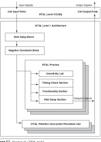
5.2 Level 1 Guidelines 63
5.2.1 Wire Delay Block 63
5.2.2 Negative Constraint Block 65
5.2.3 Processes 65
5.2.4 VITAL Primitives 70
5.2.5 Concurrent Procedure Section 70
5.3 Summary 70
CHAPTER 6 MODELING DELAYS 73
6.1 Delay Types and Glitches 73
6.1.1 Transport and Inertial Delays 73
6.1.2 Glitches 74
6.2 Distributed Delays 75
6.3 Pin-to-Pin Delays 75
6.4 Path Delay Procedures 76
6.5 Using VPDs 82
6.6 Generates and VPDs 83
6.7 Device Delays 83
6.8 Backannotating Path Delays 88
6.9 Interconnect Delays 89
6.10 Summary 90
CHAPTER 7 VITAL TABLES 91
7.1 Advantages of Truth and State Tables 91
7.2 Truth Tables 92
7.2.1 Truth Table Construction 92
7.2.2 VITAL Table Symbols 92
7.2.3 Truth Table Usage 93
7.3 State Tables 97
7.3.1 State Table Symbols 97
7.3.2 State Table Construction 97
7.3.3 State Table Usage 98
7.3.4 State Table Algorithm 99
7.4 Reducing Pessimism 100
7.5 Memory Tables 101
7.5.1 Memory Table Symbols 101
7.5.2 Memory Table Construction 102
7.5.3 Memory Table Usage 103
7.6 Summary 105
CHAPTER 8 TIMING CONSTRAINTS 107
8.1 The Purpose of Timing Constraint Checks 107 8.2 Using Timing Constraint Checks in VITAL Models 108
8.2.1 Setup/Hold Checks 108
8.2.2 Period/Pulsewidth Checks 112
8.2.3 Recovery/Removal Checks 114
8.2.4 Skew Checks 117
8.3 Violations 121
8.4 Summary 122
PART III
MODELING BASICS
123
CHAPTER 9 MODELING COMPONENTS WITH REGISTERS 125
9.1 Anatomy of a Flip-Flop 125
9.1.1 The Entity 125
9.1.3 A VITAL Process 131
9.1.4 Functionality Section 133
9.1.5 Path Delay 134
9.1.6 The “B” Side 135
9.2 Anatomy of a Latch 137
9.2.1 The Entity 138
9.2.2 The Architecture 140
9.3 Summary 146
CHAPTER 10 CONDITIONAL DELAYS AND TIMING CONSTRAINTS 147
10.1 Conditional Delays in VITAL 147
10.2 Conditional Delays in SDF 149
10.3 Conditional Delay Alternatives 150
10.4 Mapping SDF to VITAL 152
10.5 Conditional Timing Checks in VITAL 153
10.6 Summary 156
CHAPTER 11 NEGATIVE TIMING CONSTRAINTS 157
11.1 How Negative Constraints Work 157
11.2 Modeling Negative Constraints 158
11.3 How Simulators Handle Negative Constraints 176
11.4 Ramifications 177
11.5 Summary 178
CHAPTER 12 TIMING FILES AND BACKANNOTATION 179
12.1 Anatomy of a Timing File 179
12.1.1 Header 179
12.1.2 Body 181
12.1.3 FMFTIME 181
12.2 Separate Timing Specifications 182
12.3 Importing Timing Values 183
12.4 Custom Timing Sections 183
12.5 Generating Timing Files 184
12.6 Generating SDF Files 184
12.7 Backannotation and Hierarchy 185
12.8 Summary 187
PART IV
ADVANCED MODELING
189
CHAPTER 13 ADDING TIMING TO YOUR RTL CODE 191
13.1 Using VITAL to Simulate Your RTL 191
13.2 The Basic Wrapper 192
13.3 A Wrapper for Verilog RTL 206
13.4 Modeling Delays in Designs with Internal Clocks 206
13.5 Caveats 207
13.6 Summary 208
CHAPTER 14 MODELING MEMORIES 209
14.1 Memory Arrays 209
14.1.1 The Shelor Method 210
14.1.2 The VITAL_Memory Package 210
14.2 Modeling Memory Functionality 211
14.2.1 Using the Behavioral (Shelor) Method 211
14.2.2 Using the VITAL2000 Method 223
14.3 VITAL_Memory Path Delays 231
14.4 VITAL_Memory Timing Constraints 232
14.5 PreLoading Memories 235
14.5.1 Behavioral Memory PreLoad 235
14.5.2 VITAL_Memory PreLoad 237
14.6 Modeling Other Memory Types 238
14.6.1 Synchronous Static RAM 238
14.6.2 DRAM 241
14.6.3 SDRAM 244
CHAPTER 15 CONSIDERATIONS FOR COMPONENT MODELING 251
15.1 Component Models and Netlisters 251
15.2 File Contents 253
15.3 Generics Passed from the Schematic 253
15.3.1 Timing Generics 253
15.3.2 Control Generics 253
15.4 Integrating Models into a Schematic Capture System 254
15.4.1 Library Structure 254
15.4.2 Technology Independence 255
15.4.3 Directories 255
15.4.4 Map Files 256
15.5 Using Models in the Design Process 256
15.5.1 VHDL Libraries 257
15.5.2 Schematic Entry 257
15.5.3 Netlisting the Design 258
15.5.4 VHDL Compilation 258
15.5.5 SDF Generation 259
15.5.6 Simulation 261
15.5.7 Layout 261
15.5.8 Signal Analysis 262
15.5.9 Timing Backannotation 262
15.5.10 Timing Analysis 262
15.6 Special Considerations 262
15.6.1 Schematic Considerations 262
15.6.2 Model Considerations 263
15.7 Summary 266
CHAPTER 16 MODELING COMPONENT-CENTRIC FEATURES 269
16.1 Differential Inputs 269
16.2 Bus Hold 279
16.3 PLLs and DLLs 282
16.4 Assertions 284
16.5 Modifying Behavior with the TimingModel Generic 285
16.6 State Machines 285
16.7 Mixed Signal Devices 288
16.8 Summary 294
CHAPTER 17 TESTBENCHES FOR COMPONENT MODELS 295
17.1 About Testbenches 295
17.1.1 Tools 295
17.2 Testbench Styles 296
17.2.1 The Empty Testbench 296
17.2.2 The Linear Testbench 296
17.2.3 The Transactor Testbench 296
17.3 Using Assertions 297
17.4 Using Transactors 298
17.5 Testing Memory Models 301
PREFACE
Digital electronic designs continue to evolve toward more complex, higher pincount components operating at higher clock frequencies. This makes debugging board designs in a lab with a logic analyzer and an oscilloscope considerably more difficult than in the past. This is because signals are becoming physically more difficult to probe and because probing them is more likely to change the operation of the circuit. Much of the custom logic in today’s products is designed into ASICs or FPGAs. Although this logic is usually verified through simulation as a standard part of the design process, the interfaces to standard components on the board, such as memories and digital signal processors, often go unsimulated and are not verified until a prototype is built.
Waiting to test for problems this late in the design process can be expensive, however. In terms of both time and resources, the costs are higher than perform-ing up-front simulation. The decision not to do up-front board simulation usually centers around a lack of models and methodology. In ASIC and FPGA Verification: A Guide to Component Modeling, we address both of these issues.
Historical Background
The current lack of models and methodology for board-level simulation is, in large part, due to the fact that when digital simulation started to become popular in the 1980s, the simulators were all proprietary. Every Electronic Design Automation (EDA) vendor had their own and it was not possible to write models that were portable from one tool to another. They offered tools with names like HILO, SILO, and TEGAS. Most large corporations, like IBM, had their own internal simulators. At the ASIC and later FPGA levels each foundry had to decide which simulators they would support. There were too many simulators available for anyone to support them all. Each foundry had to validate that the models they provided worked correctly on each supported release of their chosen simulators.
At the board level, the component vendors saw it was impractical to support all the different simulators on the market. Rather than choose sides, they generally
decided not to provide models at all. This led to the EDA vendors trying to provide models. After all, what good is a simulator if the customer has nothing to simulate? So, each EDA vendor produced its own library of mostly the same models: 7400 series TTL, 4000 series CMOS, a few small memories, and not much else. In those days, that might be the majority of the parts needed to complete a design. But there were always other parts used and other models needed. Customers wanting to run a complete simulation had to model the rest of the parts themselves.
Eventually, someone saw an opportunity to sell (or rent) component models to all the companies that wanted to simulate their designs but did not want to create all the models required. A company (Logic Automation) was formed to lease models of off-the-shelf components to the groups that were designing them into new products. They developed the technology to model the components in their own internal proprietary format and translate them into binary code specific to each simulator.
Verilog, VHDL, and the Origin of VITAL
Verilog started out as another proprietary simulator in 1984 and enjoyed consid-erable success. In 1990, Cadence Design Systems placed the language in the public domain. It became an IEEE standard in 1995.
VHDL was developed under contract to the U.S. Department of Defense. It became an IEEE standard in 1987. Whereas Verilog is a C-like language, it is clear that VHDL has its roots in Ada. For many years there was intense competition between Verilog and VHDL for mind share and market share. Both languages have their strong points. In the end, most EDA companies came out with simulators that work with both.
Early in the language wars it was noted that Verilog had a number of built-in, gate-level primitives. Over the years these had been optimized for performance by Cadence and later by other Verilog vendors. Verilog also had a single defined method of reading timing into a simulation from an external file.
VHDL, on the other hand, was designed for a higher level of abstraction. Although it could model almost anything Verilog could, and without primitives, it allowed things to be modeled in a multitude of ways. This made performance opti-mization or acceleration impractical. VHDL was not successfully competing with Verilog-XL as a sign-off ASIC simulator. The EDA companies backing VHDL saw they had to do something. The something was named VITAL, the VHDL Initiative toward ASIC Libraries.
The VITAL Specification
these primitives were now in a standard package known to the simulator writers, they could be optimized by the VHDL compilers for faster simulation.
The timing package provided a standard, acceleratable set of procedures for checking timing constraints, such as setup and hold, as well as pin-to-pin propa-gation delays. The committee writing the VITAL packages had the wisdom to avoid reinventing the wheel. They chose the same SDF file format as Verilog for storing and annotating timing values.
SDF is the Standard Delay Format, IEEE Standard 1497. It is a textual file format for timing and delay information for digital electronic designs. It is used to convey timing and delay values into both VHDL and Verilog simulations. (SDF is discussed in greater detail in Chapter 4.)
Another stated goal of VITAL is model maintainability. It restricts the writer to a subset of the VHDL language and demands consistant use of provided libraries. This encourages uniformity among models, making them easily readable by anyone familiar with VITAL. Reabability and having the difficult code placed in a provided library greatly facilitate the maintainence of models by engineers who are not the original authors.
VITAL became IEEE Standard 1076.4 in 1995. It was reballoted in 2000. The 2000 revision offers several enhancements. These include support for multisource inter-connect timing, fast path delay disable, and skew constraint timing checks. However, the most important new feature is the addition of a new package to support the modeling of static RAMs and ROMs.
The Free Model Foundry
In 1994 I was working at TRW in Redondo Beach California as a CAE manager. The benefits of board-level simulation were clear but models were not available for most of the parts we were using. I had written models for the Hilo simulator and then rewritten them for the ValidSim simulator and I knew I would have to write them again for yet another simulator. I did not want to waste time writing models for another proprietary simulator.
At this time VITAL was in its final development and a coworker, Russ Vreeland, convinced me to look at it. I had already tried Verilog and found it did not work well at the board level. Although the show-stopper problems were tool related, such as netlisting, and have since been fixed, other problems remain with the language itself. These include (but are not limited to) a lack of library support and the inabil-ity to read the strength of a signal. My personal opinion is that Verilog is fine for RTL simulation and synthesis but a bit weak at board- and system-level modeling. All that may be changed by SystemVerilog.
In 1994, VITAL seemed to have everything I needed to model off-the-shelf com-ponents in a language that was supported by multiple EDA vendors. Russ figured out how to use it for component models, developed the initial style and method-ology, and wrote the first models. VHDL/VITAL seemed to be the answer to our modeling problem.
But TRW was in the business of developing products, not models. We felt that models should be supplied by the component vendors just as data sheets were. We suggested this to a few of our suppliers and quickly realized it was going to take a long time to convince them. In the mean time we thought we could show other engineers how our modeling techniques worked and share models with them.
In 1995, Russ Vreeland, Luis Garcia, and I cofounded the Free Model Foundation. Our hope was to do for simulation models what the Free Software Foundation had done for software: promote open source standards and sharing. We incorporated as a not-for-profit. Along the way the state of California insisted that we were not a “foundation” in their interpretation of the word. We decided we would rather switch than fight and renamed the organization the Free Model Foundry (FMF).
Today, FMF has models with timing covering over 7,000 vendor part numbers. All are free for download from our website at www.eda.org/fmf/. The models are generally copyrighted under the Free Software Foundation’s General Public License (GPL). Most of the examples in this book are taken from the FMF Web site.
Structure of the Book
ASIC and FPGA Verification: A Guide to Component Modeling is organized so that it can be read linearly from front to back. Chapters are grouped into four parts: Intro-duction, Resources and Standards, Modeling Basics, and Advanced Modeling. Each part covers a number of related modeling concepts and techniques, with individ-ual chapters building upon previous material.
Part I serves as an introduction to component models and how they fit into board-level verification. Chapter 1 introduces the idea of board-level verification. It defines component models and discusses why they are needed. The concept of technology-independent modeling is introduced, as well as how it fits in the FPGA and ASIC design flow. Chapter 2 provides a guided tour of a basic component model, including how it differs from an equivalent synthesizable model.
Part II covers the standards adhered to in component modeling and the many supporting packages that make it practical. Chapter 3 covers several IEEE and FMF packages that are used in writing component models. Chapter 4 provides an overview of SDF as it applies to component modeling. Chapter 5 describes the organization and requirements of VITAL models. Chapter 6 describes the details of modeling delays within and between components. Chapter 7 deals with VITAL truth tables and state tables and how to use them. In Chapter 8, the basics of modeling timing constraints are described.
Part III puts to use the material from the earlier chapters. Chapter 9 deals with modeling devices containing registers. Chapter 10 details the use of conditional delays and timing constraints. Chapter 11 covers negative timing constraints. Chapter 12 discusses the timing files and SDF backannotation that make the style of modeling put forth here so powerful.
around an FPGA RTL model so it can be used in a board-level simulation. Chapter 14 covers the two primary ways of modeling memories. Chapter 15 looks at some things to consider when writing models that will be integrated into a schematic capture system. Chapter 16 describes a number of different features encountered in commercial components and how they can be modeled. Chapter 17 is a discus-sion of techniques used in writing testbenches to verify component models.
Intended Audience
This book should be valuable to anyone who needs to simulate digital designs that are not contained within a single chip. It covers the creation and use of a particu-lar type of model useful for verifying ASIC and FPGA designs and board-level designs that use off-the-shelf digital components. Models of this type are based on VHDL/VITAL and are distinguished by their inclusion of timing constraints and propagation delays. The numeric values used in the constraints and delays are external to the actual models and are applied to the simulation through SDF annotation.
The intent of this book is show how ASICs and FPGAs can be verified in the larger context of a board or system. To improve readability, the phrase “ASICs and FPGAs” will be abbreviated to just FPGAs. However, nearly everything said about FPGA verification applies equally to ASIC verification.
This book should also be useful to engineers responsible for the generation and maintenance of VITAL libraries used for gate-level simulation of ASICs and FPGAs. Component vendors that provide simulation models to their customers are able to take advantage of some important opportunities. The more quickly a customer is able to verify a design and get it into production, the sooner the vendors receive volume orders for their parts. The availability of models may even exert an influ-ence over which parts, from which vendors, are designed into new products. Thus, the primary purpose of this book is to teach how to effectively model complex off-the-shelf components. It should help component vendors, or their contractors, provide models to their customers. It should also help those customers understand how the models work. If engineers are unable to obtain the models they need, this book will show them how to create their own models.
Readers of this book should already have a basic understanding of VHDL. This book will cover the details of modeling for verification of both logic and timing. Because many people must work in both Verilog and VHDL, it will show how to use VHDL component models in the verification of FPGAs written in Verilog.
The modeling style presented here is for verification and is not intended to be synthesizable.
Resources for Help and Information
Although this book attempts to provide adequate examples of models and tips on using published VHDL packages, most models and packages are too lengthy to be
included in a printed text. All of the models discussed in this book are available in their entirety from the Free Model Foundry Web site (www.eda.org/fmf/). The full source code for the IEEE packages discussed should have been provided with your VHDL simulator. They may also be ordered from the IEEE at standards.ieee.org. Addi-tional material may be found at www.mkp.com/companions/0125105819.Although I have been careful to avoid errors in the example code, there may be some that I have missed. I would be pleased to hear about them, so that I can correct them in the online code and in future printings of this book. Errata and general comments can be emailed to me at [email protected].
Acknowledgments
Very little in this book constitutes original thoughts on my part. I have merely applied other people’s ideas. Russ Vreeland developed the concept of using VITAL for component modeling. That idea has formed the basis for not just this book but for the Free Model Foundry. Ray Steele took the idea, expanded it, and applied the notion of a rigorously enforced style. Yuri Tatarnikov showed us the basics of how to use VITAL to model complex components.
I would like to thank Peter Ashenden for publishing his VHDL Cookbook on the Internet. It was my introduction to VHDL back when there was nothing else avail-able. Larry Saunders taught the first actual VHDL class I attended. I hope I do not ruin his reputation with this book.
Ray Ryan provided training on VITAL prior to it becoming a standard. His material was often referred to during the course of writing this book. His classes were instrumental in convincing Russ and I that VITAL would solve most of our technical problems regarding component modeling.
David Lieby patiently reviewed the first drafts of the book and weeded out all the really embarrassing errors. Additional valuable reviewers were Russ Vreeland, Ray Steele, Hardy Pottinger, Predrag Markovic, Bogdan Bizic, Yuri Tatarnikov, Randy Harr, and Larry Saunders.
Nate McFadden provided critical review of the logical structure of the text and smoothed the rough edges of my prose.
Part I provides a brief introduction to the board-level verification of FPGAs. The justification for the effort that goes into component modeling and the advantages of board-level simulation are discussed. Ideas for reducing the effort involved in component modeling are explored. In addition, we look at the different levels of abstraction at which models are written and their impact on simulation performance and accuracy.
Chapter 1 introduces board-level simulation. Component models are defined and the effort required to create them justified. Hints are also given regarding how to avoid having to create them all yourself. Technology-independent modeling is described and why it belongs in your FPGA design flow.
Chapter 2 observes a simple nand gate as it slowly evolves from a small syn-thesizable model to a full-fledged component model. It discusses the importance of consistent formatting and style in component modeling and how they affect maintenance. Basic concepts of modeling are introduced.
P
A
R
T
I
1
3
C
H
A
P
T
E
R
Introduction to Board-Level
Verification
As large and complex as today’s FPGAs are, they always end up on a board. Though it may be called a “system on a chip,” it is usually part of a larger system with other chips. This chapter will introduce you to the concept of verifying the chip in the system.
In this chapter we discuss the uses and benefits of modeling and define com-ponent modeling. This is done in the context of verifying an ASIC or FPGA design. We also provide some historical background and differentiate the types of models used at different stages of digital design.
1.1
Why Models Are Needed
A critical step in the design of any electronic product is final verification. The designer must take some action to assure the product, once in production, will perform to its specification. There are two general ways to do this: prototypingand simulation.
1.1.1
Prototyping
The most obvious and traditional method of design verification is prototyping. A prototype is a physical approximation of the final product. The prototype is tested through operation and measurement. It may contain additional instrumentation to allow for diagnostics that will not be included in production. If the prototype performs satisfactorily, it provides proof that the design can work in production. If enough measurements are made, an analysis can be done that will provide insight into the manufacturing yield.
1.1.2
Simulation
The other method of design verification is simulation. Simulation attempts to create a virtual prototype by collecting as much information as is known or considered pertinent about the components used in the design and the way they are con-nected. This information is put into an appropriate set of formats and becomes a model of the board or system. Then, a program, the simulator, executes the model and shows how the product should behave. The designer usually applies a stimu-lus to the model and checks the results against the expected behavior. When dis-crepancies are found, and they usually are, the simulation can be examined to determine the source of the problem. The design is then changed and the simula-tion run again. This is an iterative process, but eventually no more errors are found and a prototype is built.
Simulation requires a large effort but in many situations it is worth the trouble for one or more of the following reasons:
• Easier debugging It is easier to find the source of a problem in a virtual pro-totype than in a physical propro-totype. In the model, all nodes are accessible. The simulator does not suffer from physical limitations such as bandwidth. Observing a node does not alter its behavior.
• Faster, cheaper iterations When a design error is identified, the model can be quickly fixed. A physical prototype could require months to rebuild and cost large sums of money.
• Virtual components can be used A virtual prototype can be constructed using models of components that are not yet available as physical objects.
• Component and board process variations and physical tolerances can be explored A physical prototype can embody only a single set of process vari-ations. A virtual prototype can used to explore design behavior across a full range of variations.
• Software development can begin sooner Diagnostic and embedded soft-ware development can begin using the virtual prototype. The interplay between hardware and software development often shows areas where the design could be improved while there is still time to make changes.
For FPGA design, nearly everyone simulates the part they are designing. The FPGA vendor provides models of simulation primitives(cell models), the lowest-level structures in the design that the designer is able to manipulate. There are usually between 100 and 300 of these relatively simple primitives in an FPGA library. The silicon vendor supplies them because everyone agrees simulation is required and it is a reasonably sized task.
provide simulation models (although the number is slowly growing). Design groups must often write their own models. Unlike the FPGA primitives, each component needs to be modeled, and these models can be very large. In the end, many designers build prototypes. They then test them in the lab, as best they can, and build new prototypes to correct the errors that are found rather than performing the more rigorous simulations.
It has been said that the beauty of FPGAs is that you don’t have to get them right the first time. This is true. However, you do have to get them right eventu-ally. The iterative process of design and debug has a much faster cycle time when it is simulation based rather than prototype based. Not just the prototyping time is saved. The actual debug is much faster using a simulation than using a physical board, as illustrated in Figure 1.1. This is becoming even more true as boards incorporate larger, finer-pitched, ball grid array components.
1.2
Definition of a Model
For the purposes of this book, a model is a software representation of a circuit, a circuit being either a physical electronic device or a portion of a device. This book concentrates exclusively on models written in VHDL but it includes methods for incorporating Verilog code in a mixed-language verification strategy.
In modeling, there are different levels of abstraction and there are different types of models. The two are related but not quite the same thing. Think of a design being conceived of at a level of abstraction and modeled using a particu-lar model type. It is always easier to move from higher to lower levels of abstrac-tion than to move up. Likewise, it is difficult to model a component using a model type that is at a higher level than the data from which the model is being created.
1.2 Definition of a Model 5
Design 1 Day
Simulation Cycle Time Debug
1 Hour
Simulate 1 Hour
Design 1 Day
Prototype Cycle Time Debug
1 Day
Prototype 1 Week
1.2.1
Levels of Abstraction
All digital circuits are composed primarily of transistors. Modern integrated circuits contain millions and soon billions of these transistors. Transistors are analog devices. In digital circuits they are used in a simplified manner, as switches. Still, they must be designed and analyzed in the analog domain.
Analog simulation is very slow and computationaly intensive. To simulate mil-lions of transistors in the analog domain would be exceedingly slow, complex, and not economically practical. Therefore, like most complex problems, this one is attacked hierarchically. Each level of hierarchy is a level of abstraction. Small groups of tran-sistors are used to design simple digital circuits like gates and registers. These are small enough to be easily simulated in the analog domain and measured in the lab. The results of the analog simulations are used to assign overall properties, such as propa-gation delays and timing constraints to the gates. This is referred to as characterization. The characterized gates can then be used to design more complex circuits, coun-ters, decoders, memories, and so on. Because the gates of which they are composed are characterized, the underlying transistors can be largely ignored by the designer. This process is extended so that still more complex products such as micro-processors and MPEG decoders can be designed from counters and instruction decoders. Computers and DVD players are then designed from microprocessors and MPEG decoders. This hierarchical approach continues into the design of global telecommunications networks and other planet-scale systems.
We will follow this process by discussing models starting at the gate level of com-plexity and going up through some of the more complex single integrated circuits.
Gate Level
Gate-level models provide the greatest level of detail for simulation of digital cir-cuits and are the lowest level of abstraction within the digital domain. Gate-level simulation is usually a requirement in the ASIC design process. For FPGAs and ASICs, the library of gate-level models is provided by the component vendor or foundry. The gate-level netlist can be derived from schematics but more often is synthesized from RTL code.
Because it includes so much detail, gate-level simulation tends to be slower than register transfer level (RTL) or behavioral simulation. However, because gate-level models are relatively simple, several EDA vendors have created hardware or soft-ware tools for accelerating simulations beyond the speeds available from general-purpose HDL simulators.
RTL
a synthesis engine. The synthesis engine then decomposes the RTL description to a gate-level description that can be used to create an ASIC layout or to generate a program for an FPGA.
The person writing the RTL description is concerned primarily with the circuit’s interior function. He can specify details such as the type of carry chain used in an adder or the encoding scheme used in a state machine. For the designer, the chip is the top level of the design. When the RTL is used in simulation, it will usually be the device under test (DUT).
RTL models can and should be simulated. This verifies the functionality of the code. However, the RTL code, as written for synthesis, does not include any delay or timing constraint information. Of course, delays could be included but until a physical implementation has been determined the numbers would not be accurate. Accurate timing comes from simulating the chip at the gate level.
Behavioral
In contrast to lower-level models, behavioral models provide the fewest details and represent the highest level of abstraction discussed in this book. The purpose of a behavioral model is to simulate what happens on the edge of a chip or cell. The user wants to see what goes in and what comes out and does not care about how the work is done inside. If delays are modeled, they are modeled as pin-to-pin delays.
The reduced level of detail allows behavioral models to generally run much faster than either gate-level or RTL models. They are also much easier to write, assuming a high-level description of the component is available.
Looking from this perspective, models of off-the-shelf components should be written at the behavioral level whenever possible. Besides being faster to write and faster to run, they give away little or no information about how a part is designed and built. They are inherently nonsynthesizable and do not disclose intellectual property (IP) beyond what is published in the component’s data sheet.
Bus Functional
Bus functional models (BFMs) are usually created for very complex parts for which a full behavioral model would be too expensive to create or too slow to be of value. BFMs attempt to model the component interface without modeling the component function. They are not complete enough to simulate running software but they are adequate for verifying that the component is correctly designed into the larger system. Microprocessors and digital signal processors are candidates for bus functional models.
1.2.2
Model Types
There are three types of HDL models in common use: cell, RTL, and behavioral. Component models are usually a special case of behavioral models.
Cell
Cell models describe the functionality of the cells in the gate-level netlist. They are provided in libraries by FPGA vendors and are usually specific to a particular FPGA family. Cell models include propagation delays and timing constraints. However, the actual delay and constraint values are not coded directly into the models. Instead, these values are calculated by software usually provided by the FPGA vendor. The calculated values are then written to an SDF file and annotated into the simulation. Cell models are commonly of low to medium complexity.
RTL
The RTL model is used to describe a digital circuit a designer intends to synthesize. RTL models do not include timing. They are also used to simulate a design prior to synthesis. RTL models contain no information regarding propagation delays or timing constraints. A synthesis engine converts an RTL model into a gate-level netlist for a targeted FPGA. The gate-level netlist then instantiates a number of gates or cells and describes how they are connected to each other, as shown in Figure 1.2.
Behavioral
Behavioral models describe what a circuit or system does without attempting to explain how it does it. They are written with the fewest constraints: They may or may not be synthesizable, they may or may not include timing, and they may or may not be cycle accurate. They may be intended for use in architectural exploration, performance modeling, or hardware/software codesign.
Behavioral model development is not limited to VHDL and Verilog. They may be written in general computing languages such as C/C++ or any of the special
system-level languages, such as Esterel or Rosetta.
CELLS
D0 RTL
IF CLK’EVENT AND CLK = ‘1’ THEN IF SEL = ‘0’ THEN
Q <= DO; ELSE Q <= D1; END IF; END IF;
D1
SEL synthesis
CLK Q
Component
Component models are models of off-the-shelf components used in board-level design. They use the same techniques for describing propagation delays and timing constraints as cell models. Models of simple components are constructed in the same manner as models of simple gates. Components, however, can be much more complex than gates. Complex components are modeled using a mixture of behav-ioral, RTL, and gate-level techniques with the intent of including as little detail as required to produce the correct behavior at the component interface. Sometimes, only their interfaces are modeled, in which case they may be referred to as BFMs. It is possible to create a component model for an FPGA by embedding an RTL model in a wrapper that provides pin-to-pin propagation delays and timing con-straint checks. Such a model can be used to accelerate the simulation of a board or system containing one or more large, user-designed components. A model constructed in this manner will provide much of the functionality of a gate-level model but execute at the speed of a RTL model. Figure 1.3 illustrates how the RTL code from Figure 1.2 might be incorporated into a component model.
1.2.3
Technology-Independent Models
Creating component models is work, and unless you work for a component vendor, it may not be your primary responsibility. Most often, you would like to write as few models as necessary to accomplish your verification goals. The best way to reduce the number of models needed is to make them technology (timing) independent.
The core concept is the separation of timing and behavior. In this method the VHDL (or Verilog) model describes component behavior but contains no timing
1.2 Definition of a Model 9
Q
CLK INPUT DELAYS
SEL TIMING CONSTRAINT
CHECKS
OUTPUT DELAYS
FUNCTIONALITY BEHAVIORAL, RTL, or BFM D1
D0
information. All timing values, for delays and constraints, reside in a separate ASCII file. A single model may represent many parts that differ only in timing. A single timing file contains all the different timings for that model. A tool is used to extract the desired timing from all the timing files for all the models and generate an SDF file for the entire design.
1.3
Design Methods and Models
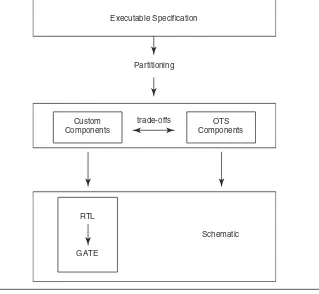
There are many design methods that use the various type of models described here. One such method is the classic top-downstyle. In this method, a behavioral model of the system to be designed is written and simulated. It is modified until it ade-quately describes the desired product. It then becomes an executable specification for the design against which the design implementation can be compared. The design is then partitioned into sections that will be custom built with ASICs and FPGAs and sections that will be built with off-the-shelf (OTS) components (if any). There may be trade-off studies done to determine the optimum partitioning between custom and OTS hardware.
The custom section is further partitioned into as many different custom components as required and each of those is coded at the register-transfer level and synthesized to gates. The OTS section is designed using schematics. The custom parts are added to the schematic and, if models are available of the OTS parts, the system can be simulated to verify that all the components, including the custom ones, are correctly connected and will perform the desired functions. This method is shown in Figure 1.4.
The top-down method seems best suited for designs that have rigid performance requirements. These designs could be for defense or commercial markets that are performance driven and have very high volumes.
Another, more common approach may be called either bottom-upor outside-in. In this method performance goals are tempered by cost considerations. Instead of an executable specification, the design exploration may begin with the question, “How good can we make it and still meet our cost goals?” In such environments, custom components are designed only when they will be more cost effective than off-the-shelf components. Component availability can strongly influence the architecture of this type of product.
A representation of the bottom-up method is shown in Figure 1.5.
In both of the described methods, there is a point at which custom-designed components, ASICs and FPGAs, must be integrated with off-the-shelf components. Verifying correct integration is where component models come into the picture.
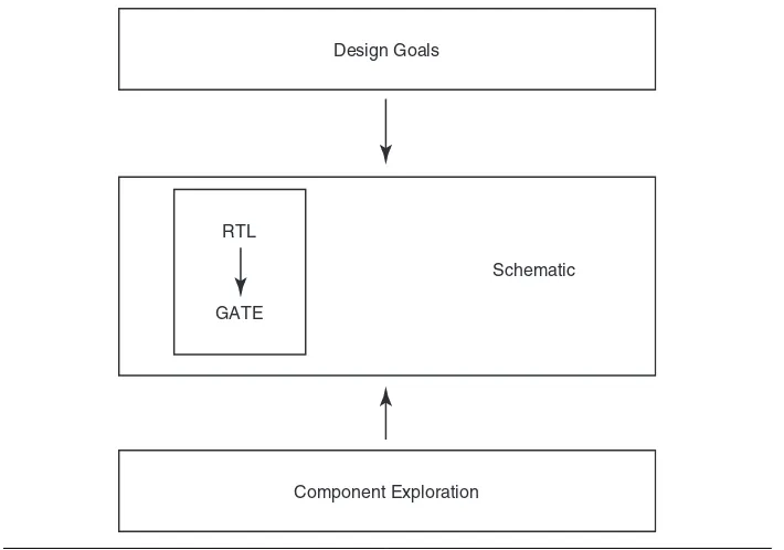
1.4
How Models Fit in the FPGA/ASIC Design Flow
most of the verification effort goes into proving that the internal logic of the custom part meets its specification, its interfaces with the rest of the system must be correct for it to contribute to a working product. Simulating these interfaces is most easily done by using models of the surrounding components.
Even when verifying the FPGA’s internal logic, external component models may be used. A testbench may be more accurate and easier to construct if it incorpo-rates models of peripheral components. These models can prove particularly helpful in uncovering errors in power up, reset, and boundary conditions.
1.4.1
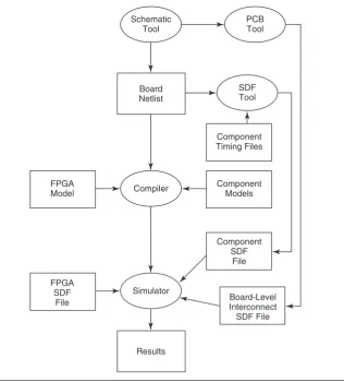
The Design/Verification Flow
For FPGA-on-board verification, FPGAs are designed in VHDL or Verilog. They can be modeled at the behavioral level, RTL, or gate level. The boards they go into are designed using a schematic capture system. Schematics are still used for board design because they are a convenient and effective method of entering and con-veying information about the logic and physical characteristics of a design. The
1.4 How Models Fit in the FPGA/ASIC Design Flow 11
Executable Specification
Custom Components
OTS Components
RTL
GATE
Schematic Partitioning
trade-offs
schematic tool generates a VHDL netlist and other files needed to interface with a printed circuit board (PCB) layout tool. The components on the board are laid out and the connections between them routed in the PCB tool.
At this point, the FPGA has a model, the other components on the board have models, and the netlist describes how they are connected. All of these are fed to the HDL analyzer/compiler.
In addition to models describing their logical operation, these components have timing files. An SDF extraction tool reads the netlist and the timing files to create an SDF file with timing for all the components that are in the netlist. The FPGA may have its own SDF file, and still another SDF file can be generated by the PCB layout tool, or a signal integrity tool, to describe the interconnect delays.
The SDF file(s) and the compiled models are read by the simulator. A testbench provides the stimulus. The results are examined by the design engineer and the necessary changes are made to the board and/or FPGA design. This process is repeated until no more errors are found or it is otherwise determined to build the first prototype. This, of course, does not mean there are no more errors, just that you need to do something different to find them.
A diagram of this flow is shown in Figure 1.6. Keep it in mind as you learn to create and use component models as part of your ASIC/FPGA system verification strategy.
Design Goals
Component Exploration RTL
GATE
Schematic
1.5
Where to Get Models
For a model to have maximum utility and portability, it must be available to the engineer as source code. There are three places to get such models. Some com-ponent vendors, mostly memory suppliers, provide source code models. Micron Technology was one of the pioneers in providing simulation models to its cus-tomers directly from its Web site. IDT and AMD memory divisions have both taken up the challenge and provide models of the style presented in this book. Intel flash memory division also offers some models. Although some of the models offered are quite good, others seem to have been written for the purpose of simulating a single, stand-alone part with no provision for verifying the component in a larger design.
1.5 Where to Get Models 13
Board Netlist
Results Schematic
Tool
Compiler
PCB Tool
SDF Tool
Component Timing Files
Component Models FPGA
Model
Simulator FPGA
SDF File
Component SDF
File
Board-Level Interconnect SDF File
There are also some EDA vendors who offer models. These vary widely and may be encrypted, requiring a license or special software, or they may be in source code form. Cost and usability also vary. Most models from EDA vendors and component vendors do not allow for backannotation of interconnect delays and may not allow for SDF backannotation at all.
Writing your own models is, of course, an option. This book provides the guid-ance you need to write complete and efficient models for use in ASIC/FPGA/board verification. This book also demonstrates how to incorporate your RTL or gate-level design into the board-level simulation. For the models you are able to find on the World Wide Web, it provides insight into how the models are constructed and how to use them.
In addition, as mentioned in the preface, another source of models is the Free Model Foundry. If you do write your own models of off-the-shelf components, you might consider sharing them with others. This can be done through the Free Model Foundry.
1.6
Summary
The verification of an FPGA is not complete until it has been simulated as a com-ponent at the board level. Doing this requires having models of the off-the-shelf components to which it is connected. These component models are quite different from the RTL models you write for synthesis. Some of them are available from vendor Web sites (if not, always ask for them) or from the Free Model Foundry, and others you will need to write yourself. Once you have the models, your FPGA design can be simulated at the board level to verify correct interfaces and system functionality.
2
15
C
H
A
P
T
E
R
Tour of a Simple Model
In this chapter we examine a very basic component model, a 2-input nand gate, in order to better understand the different goals of simulation and synthesis. This simple model allows us to review the basic requirements of a component model and see how such a model is different from the RTL models written for synthesis. The reason for beginning with such a trivial model is that it allows us to concen-trate on the new concepts normally present in a VITAL component model that are not found in an RTL model. (Much more complex models will be discussed later in the book.)
The synthesizable 2-input nand gate we are to examine is shown in Figure 2.1. It is part of a larger synthesizable design. Written in VHDL code, the model has an active low output and is designated as such by appending a “neg” to the end of its name. (The reason for this particular convention is explained later.) This is a per-fectly good model of a nand gate—if you are designing nand gates for synthesis only. On the other hand, if your job is to create a nand gate model that will be used as an FPGA simulation primitive or an off-the-shelf component to be used in a board-level simulation, you might find this model has some deficiencies. Let’s look more closely at this model to see how it can be enhanced with simulation in mind, our goal being to create a VHDL model for the nand gate and the SDF to accompany it.
2.1
Formatting
Also, because the parts you model are likely to reappear again in your next design, you are likely to read it too. Since you may also need to maintain it, you will want do what you can to make the model easy to edit and to understand.
Uniformity is important. If all your models are written in the same style and format, it becomes easy to navigate through them to find the section you want, and it will be easier to understand them. When you have a large number of models and a global change is required, having the models written in a consistent format may mean they can be updated using a script in batch mode instead of you having to plod through them one by one.
The first thing we can do is put a banner on the top so we can always see which file we are editing or which model we have printed. Let us make this banner 80 characters wide because 80 columns print reasonably well and we can set our window width to match the banner so we always know where to break a line.
--- File Name: ex2_nand.vhd
---Next should come the library statements. Each model is standalone and in its own file, so each one needs its own library clauses.
LIBRARY IEEE; USE IEEE.std_logic_1164.ALL;
In the entity, we will use a separate line for each port. This takes up more space but is more readable and accessible by scripts. Besides, lines are cheap.
PORT (
A : IN std_logic; B : IN std_logic; YNeg : OUT std_logic );
Let’s add another banner to separate the entity and architecture sections.
--- ARCHITECTURE DECLARATION
---Finally, we will capitalize key words and signal names so they stand out better. Some people prefer to make key words lowercase and capitalize everything else. Some are even passionate about whether key words are uppercase or lowercase. It is really just an arbitrary decision. I have chosen to use uppercase key words because that is
entity nandgate is
port (a, b : in std_logic; yneg : out std_logic); end nandgate;
architecture ex1 of nandgate is begin
yneg <= a nand b; end;
how it is done in the Institute of Electrical and Electronics Engineers (IEEE) pack-ages. Figure 2.2 shows the nand model with the added formatting.
2.2
Standard Interfaces
Multichip or board-level simulation involves more than just ones and zeros. Signals can be strong or weak or high impedance. Drivers can have open collector outputs and require pull-up resistors. Realistic simulations require at least the 9-state logic found in the IEEE 1164 package, std_ulogic. For these reasons, except for mixed signal models, ports will always be of type std_ulogic. The difference between
std_logic and std_ulogic types is that std_logic is a resolved subtype of
std_ulogic. Using std_ulogic provides a slight performance improvement during simulation. Although the improvement is actually quite small, if there are thousands of instantiations of the model (and there could be many thousands) it could become significant. Vectored ports are not used because they would inhibit backannotation of interconnect delays. Interconnect delays are discussed later in this chapter.
It is good practice to explicitly specify default initial values for all ports. At the board level, sometimes an input pin may be left unconnected. When the design is netlisted, the unconnected pin is assigned to the key word OPEN. VHDL has a restric-tion that in order to be assigned to OPEN, an input port must have an explicit default value.
PORT (
A : IN std_ulogic := ‘U’;
B : IN std_ulogic := ‘U’;
YNeg : OUT std_ulogic := ‘U’
);
2.2 Standard Interfaces 17
--- File Name: ex2_nand.vhd
---LIBRARY IEEE; USE IEEE.std_logic_1164.ALL;
ENTITY nandgate IS PORT (
A : IN std_logic; B : IN std_logic; YNeg : OUT std_logic );
END nandgate;
--- ARCHITECTURE DECLARATION
---ARCHITECTURE ex2 OF nandgate IS
BEGIN
YNeg <= A nand B; END;
In most cases the default value should be ‘U’for uninitialized, as shown. However, some parts have inputs with internal pull up or pull down resistors so that unused inputs will be pulled to a known state and may be left unconnected if not needed. These pins are given initial values of ‘1’or ‘0’as appropriate.
There is at least one other case when an output is given an initial value other than ‘U’. Some ECL logic parts have a VBB output. These pins are initialized to
‘W’for reasons discussed in Chapter 16.
2.3
Model Delays
In Figure 2.2 we have a model that would function correctly as a nand gate but has zero delay. All physical parts have some delay. Sometimes we rely on that delay, other times we would like it to go away, but we always have to account for it. So how do we add delays to our models?
The simplest way of expressing a delay in VHDL is with an AFTERclause:
YNeg<=A nand B AFTER 6 ns;
This is fine if the part you are modeling happens to switch in 6 nanoseconds, in both directions, under all conditions. But then you would have to create another model when the new 4 nanosecond (ns) part came out.
VHDL has a stock solution for such problems: generics. Generics are used to pass information into a model. When a generic is used to pass information into a model, it describes a constant and can only be read. A generic is declared in the model entity and used in the architecture. Figure 2.3 shows our model with a generic named delay.
--- File Name: ex3_nand.vhd
---LIBRARY IEEE; USE IEEE.std_logic_1164.ALL;
ENTITY nandgate IS GENERIC (
delay : TIME := 10 ns );
PORT (
A : IN std_ulogic := ‘U’; B : IN std_ulogic := ‘U’; YNeg : OUT std_ulogic := ‘U’
); END nandgate;
--- ARCHITECTURE DECLARATION
---ARCHITECTURE ex3 OF nandgate IS
BEGIN
YNeg <= A nand B AFTER delay; END;
This is an improvement. Now only one model is needed to cover many possi-ble nand gates. But the model still has symmetrical rise and fall delays that may not match the part used in your design. Most non-CMOS components use a totem-pole output structure that has different drive strengths depending on whether it is driving high or low. This causes the effective pin delay to be different for a high output than a low output.
2.4
VITAL Additions
The next several changes to the model are the addition of VITAL types, attributes, primitives, processes, or methods. By using these VITAL features, we make our models more uniform and improve their simulation performance. VITAL enables the technology independence we need to reuse models rather than constantly rewrite them.
2.4.1
VITAL Delay Types
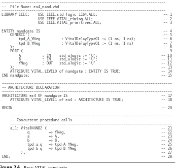
Another deficiency in the model in Figure 2.3 is that the correct value for the delay must be written into the netlist, which can be inconvenient. Although there are many ways to overcome these limitations, in Figure 2.4 we use VITAL for pin-to-pin (path) delays, which is an IEEE standard. VITAL path delay generics are recognizable by their tpdprefix. There are a number of related changes made in Figure 2.4, and as you can see, the model has grown somewhat.
On lines 2 and 3 of Figure 2.4 are two new USE clauses calling out two VITAL packages. The first package contains the VITAL timing constraint and delay rou-tines. The second package contains the VITAL accelerated primitives.
On lines 6 and 7 of Figure 2.4 are our delay generics. There is one for each input. Path delay generics (tpd) in VITAL are formed using a standardized formula. The names start with tpdand the names of the input port and output port are added in that order, all separated by underscores. Thus, the name of the generic to hold the value of the delay from pin Ato pin YNegis tpd_A_YNeg:
tpd_A_YNeg : VitalDelayType01 := (1 ns, 1 ns); -- 6 tpd_B_YNeg : VitalDelayType01 := (1 ns, 1 ns) -- 7
The type of these generics is VitalDelayType01. A generic of this type is used for paths that can cause the output to transition only between low and high. It takes two values, each is of type Time. The first is the delay for low to high transitions (LH), the second for high to low transitions (HL). The VITAL timing package also defines a type VitalDelayType01Zfor paths that can cause an output to go high impedance (‘Z’), and VitalDelayType01ZX for paths that can cause the output to go to ‘X’, the unknown. VitalDelayType01 Z takes 6 values: LH, HL, LZ, ZH, HZ, and ZL. VitalDelayType01ZX takes 12 values: LH, HL, LZ, ZH, HZ, ZL, LX, XH, HX, XL, XZ, and ZX. Definitions of the IEEE std_logic_1164logic values are given in the next chapter.
As mentioned earlier, the nand gate has an active low output, and we indicate such by appending the Negsuffix to its name in accordance to Free Model Foundry convention. Many people like to use other conventions, such as an _Lsuffix. We cannot include underscores in port names in VITAL models because underscores are used as delimiters in the generic names.
2.4.2
VITAL Attributes
Because our enhancements to the model as shown in Figure 2.4 have made this a VITAL model, we need to notify the compiler of that fact. Line 14,
ATTRIBUTE VITAL_LEVEL0 of nandgate : ENTITY IS TRUE;
tells the compiler that the model is compliant with the level 0 VITAL specification. Level 0 pertains primarily to the entity part of a model. Its purpose is to promote
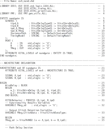
--- File Name: ex4_nand.vhd
---LIBRARY IEEE; USE IEEE.std_logic_1164.ALL; -- 1 USE IEEE.VITAL_timing.ALL; -- 2 USE IEEE.VITAL_primitives.ALL; -- 3
ENTITY nandgate IS -- 4 GENERIC ( -- 5 tpd_A_YNeg : VitalDelayType01 := (1 ns, 1 ns); -- 6 tpd_B_YNeg : VitalDelayType01 := (1 ns, 1 ns) -- 7 ); -- 8 PORT ( -- 9 A : IN std_ulogic := ‘U’; -- 10 B : IN std_ulogic := ‘U’; -- 11 YNeg : OUT std_ulogic := ‘U’ -- 12 ); -- 13 ATTRIBUTE VITAL_LEVEL0 of nandgate : ENTITY IS TRUE; -- 14 END nandgate; -- 15
--- ARCHITECTURE DECLARATION
---ARCHITECTURE ex4 OF nandgate IS -- 17 ATTRIBUTE VITAL_LEVEL1 of ex4 : ARCHITECTURE IS TRUE; -- 18
BEGIN -- 20
-- Concurrent procedure calls
a_1: VitalNAND2 ( -- 21 q => YNeg, -- 22 a => A, -- 23 b => B, -- 24 tpd_a_q => tpd_A_YNeg, -- 25 tpd_b_q => tpd_B_YNeg -- 26 ); -- 27 END; -- 28
the portability and interoperability of the model. It not only restricts the form and semantic content of the entity, but also standardizes the specification and process-ing of timprocess-ing information. It enables the model to use the VITAL backannotation and timing check routines. The simulator will be able to read an SDF file and match it up with the model.
Line 18,
ATTRIBUTE VITAL_LEVEL1 of ex4 : ARCHITECTURE IS TRUE;
tells the compiler that we also claim VITAL level 1 compliance. Level 1 allows the compiler to optimize the compiled model for faster setup and simulation. To do this, we must restrict ourselves to certain VHDL constructs. We will discuss these restrictions as we come to them.
Level 1 compliance makes the most sense for smaller models that are best described in terms of gates. The execution speed of these models will be acceler-ated by the use of VITAL level 1. Larger and more complex models are better described in a behavioral style. They may not be practical or desirable to write at the gate level and will run faster as behavioral models anyway. Level 1 compliance is optional.
A brief comparison of the VITAL compliance levels is given in Table 2.1. More details are provided in Chapters 3 and 5.
2.4.3
VITAL Primitive Call
Lines 21 through 27 of Figure 2.4,
a_1: VitalNAND2 ( -- 21
q => YNeg, -- 22
a => A, -- 23
b => B, -- 24
tpd_a_q => tpd_A_YNeg, -- 25 tpd_b_q => tpd_B_YNeg -- 26
); -- 27
2.4 VITAL Additions 21
Table 2.1 Comparison of VITAL levels
VITAL Level 0 VITAL Level 1
Provides: SDF backannotation, negative acceleration of primitives and tables timing constraints
Requires: level 0 attribute, std_ulogicand level 1 attribute, no shared variables,
std_logic_vectorports, no operators restricted to those in Standard underscores in port names, and std_logic_1164, all outputs special rules for timing generics must be driven by a VitalPathDelay or
are a concurrent procedure call to the VITAL primitive VitalNAND2. VITAL primi-tives are accelerated by the compiler and simulator for better simulation perform-ance. The ports are mapped by name. The last two arguments are the two delays, one from each input to the output. Some components may specify identical delays from each input and others may not. The VITAL primitives always require that separate delays be specified. VITAL primitives do not offer as much flexibility in handling delays as another procedure, the VitalPathDelay(VPD), but VPDs must be called from within a process.
A further improved model incorporating a VITAL process is given in Figure 2.5.
2.4.4
VITAL Processes
A VITAL process consists of the following three sections: timing constraint checks, functionality, and path delays. The sections must be in the listed order. A more complete description is found in Chapter 5.
On line 20 of Figure 2.4,
VITALBehavior : PROCESS (A, B)
we begin a VITAL process. The use of a VITAL process gives us control over a number of behaviors that would be difficult to control otherwise. These will be pointed out as we walk through the code. Line 21,
VARIABLE YNeg_zd : std_ulogic :=‘U’;
declares a functionality result variable. It will hold the zero delay result prior to it being scheduled for output. It must be a variable rather than a signal for the model to be level 1 compliant. The FMF convention, which follows examples given in the VITAL standard document, is to create the name for this variable by taking the name of the output port to which it refers and appending the characters _zd, for zero delay.
The next line, 22,
VARIABLE YNeg_GlitchData : VitalGlitchDataType;
declares the glitch variable for YNeg. Glitches and glitch handling will be covered in detail in the next chapter. For now, just be aware that a glitch variable is required for a path delay statement to be used.
The statement on line 24,
YNeg_zd := VitalNAND2 (a => A, b => B);
2.4 VITAL Additions 23
--- File Name: ex5_nand.vhd
---LIBRARY IEEE; USE IEEE.std_logic_1164.ALL; -- 1 USE IEEE.VITAL_timing.ALL; -- 2 USE IEEE.VITAL_primitives.ALL; -- 3
ENTITY nandgate IS -- 4 GENERIC ( -- 5 tpd_A_YNeg : VitalDelayType01 := (1 ns, 1 ns); -- 6 tpd_B_YNeg : VitalDelayType01 := (1 ns, 1 ns) -- 7 ); -- 8 PORT ( -- 9 A : IN std_ulogic := ‘U’; -- 10 B : IN std_ulogic := ‘U’; -- 11 YNeg : OUT std_ulogic := ‘U’ -- 12 ); -- 13 ATTRIBUTE VITAL_LEVEL0 of nandgate : ENTITY IS TRUE; -- 14 END nandgate; -- 15
--- ARCHITECTURE DECLARATION
---ARCHITECTURE ex5 OF nandgate IS -- 16 ATTRIBUTE VITAL_LEVEL1 of ex5 : ARCHITECTURE IS TRUE; -- 17 BEGIN -- 18 VITALBehavior : PROCESS (A, B) -- 20
-- Functionality Results Variables
VARIABLE YNeg_zd : std_ulogic := ‘U’; -- 21
-- Output Glitch Detection Variables
VARIABLE YNeg_GlitchData : VitalGlitchDataType; -- 22
BEGIN -- 23 YNeg_zd := VitalNAND2 (a => A, b => B); -- 24
-- Path Delay Section
VitalPathDelay01 ( -- 25 OutSignal => YNeg, -- 26 OutSignalName => “YNeg”, -- 27 OutTemp => YNeg_zd, -- 28 Paths => ( -- 29 0 => (InPutChangeTime => A’LAST_EVENT, -- 30 PathDelay => tpd_A_YNeg, -- 31 PathCondition => TRUE ), -- 32 1 => (InPutChangeTime => B’LAST_EVENT, -- 33 PathDelay => tpd_B_YNeg, -- 34 PathCondition => TRUE ) ), -- 35 GlitchData => YNeg_GlitchData ); -- 36 END PROCESS; -- 37 END; -- 38
2.4.5
VitalPathDelays
For VITAL level 1 compliance, all output ports must be driven by a procedure call to either a VitalPathDelayor a VITAL primitive.
YNeg_zd is not assigned directly to the output port. The assignment is done through the VitalPathDelay01 procedure beginning on Figure 2.4, line 25,
VitalPathDelay01 (
If there were more than one output port, this procedure would be called for each 2-state output port. Let us examine the call, line by line:
OutSignal => YNeg, -- 26
OutSignalName => “YNeg”, -- 27
OutTemp => YNeg_zd, -- 28
OutSignalgets the name of the port to which the result is ultimately assigned. OutSignalNamegets a string that is the name of the port as you would like it stated in any error messages that may be generated by the procedure. OutTempgets the variable that holds the temporary result of the functional simulation. Despite its name, remember it is an input to the procedure.
Line 29,
Paths => ( -- 29
0 => (InPutChangeTime => A’LAST_EVENT, -- 30 PathDelay => tpd_A_YNeg, -- 31 PathCondition => TRUE ), -- 32 1 => (InPutChangeTime => B’LAST_EVENT, -- 33 PathDelay => tpd_B_YNeg, -- 34 PathCondition => TRUE ) ), -- 35
is the beginning of the Pathssection. For each possible path from each input to the output there are three lines. The three lines constitute a VHDL record. The records elements are:
InputChangeTime: The time of the last change on an input that may have triggered the process we are in.
PathDelay: The set of delays to apply to the output, for this path.
PathCondition: The condition that must be met for this path to be considered valid. It may be a boolean expression and must evaluate to true for this path to be selected.
Together, all the paths become an array of recor