Gate Dielectric Scaling for High-Performance CMOS: from SiO
2to High-K
Robert Chau, Suman Datta, Mark Doczy, Jack Kavalieros and Matthew Metz
Intel Corporation
5200 N.E. Elam Young Parkway, Hillsboro, OR 97124, USA. Mail-stop: RA3-252 503-613-6141, [email protected]
Abstract
We have successfully demonstrated very high-performance PMOS and NMOS transistors with high-K/metal-gate gate stacks with the right threshold voltages for both p- and n-channels on bulk Si. We believe that high-K/metal-gate is an option for the 45nm high-performance logic technology node.
1. Introduction
The silicon industry has been scaling SiO2 aggressively for
the past 15 years for low-power, high-performance CMOS logic applications. SiO2 as thin as 1.2nm (physical Tox) has
already been successfully implemented in the 90nm logic technology node [ref. 1]. Research transistors with 0.8nm SiO2 have also been demonstrated in the laboratory [ref. 2-3].
However, continual gate dielectric scaling will require high-K, as SiO2 will eventually run out of atoms for further
scaling. Most of the high-K gate dielectrics investigated are Hf-based and Zr-based [ref. 4-6]. Both polySi and metals are being evaluated as gate electrodes for the high-K dielectrics [ref. 7-9]. There are many challenges reported in literature in replacing SiO2 with high-K for high-performance CMOS [ref.
10-12]. This paper will present results on the 0.8nm SiO2 and
very high-performance PMOS and NMOS transistors with high-K/metal-gate for high-performance logic applications.
2. SiO2 Scaling
The physical thickness of SiO2 has been scaled aggressively
for low-power, high-performance logic applications. Figure 1 shows the physical thickness trend of SiO2 for the various
logic generations. 1.2nm physical SiO2 has already been
successfully implemented in the 90nm logic node [ref. 1]. In addition, 0.8nm physical SiO2 has also been produced [ref. 2-3]. TEM cross sections of the 1.2nm and 0.8nm SiO2 gate
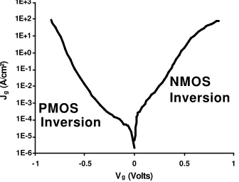
oxides are shown in Figures 2-3. The electrical C-V and Ig-Vg characteristics of the 0.8nm SiO2 are shown in Figures
4-5. Figures 6-7 show the device characteristics of the experimental 15nm (physical gate length) NMOS transistor with 0.8nm SiO2. The data shows that the 15nm transistor
with 0.8nm physical SiO2 has well-controlled short -channel
characteristics.
3. High-K Dielectrics
It has been reported in literature [ref. 12] that Fermi level pinning at the high-K/polySi interface causes high threshold voltages in MOSFET transistors. It has also been reported that high-K/polySi transistor exhibits severely degraded channel mobility due to the coupling of low energy surface
optical (SO) phonon modes arising from the polarization of the high-K to the inversion channel charge carriers [ref. 13], and that metal gate may be more effective in screening the high-K SO phonons from coupling to the channel under inversion conditions [ref. 13-14]. On the other hand, the use of high-K/metal-gate requires a p-type metal and a n-type metal with the right work functions for high-performance CMOS logic applications on bulk Si [ref. 15].
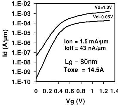
We have successfully fabricated high-performance PMOS and NMOS transistors with high-K/metal-gate stacks. The transistors have physical gate length (Lg) of 80nm and the electrical oxide thickness (Toxe) is 1.45nm measured at inversion. Figure 8 compares the leakage characteristics of the high-K/metal-gate stacks with the conventional SiO2/polySi. Figures 9-10 show the device characteristics of
the PMOS transistor with high-K/metal-gate, while Figures 11-12 show the device characteristics of the NMOS transistor with high-K/metal-gate. Both the high-K/metal-gate PMOS and NMOS transistors show very high drive performance (Idsat) with the right Vth for both p- and n-channel devices on bulk Si, with very low gate leakage.
4. From SiO2 to High-K
We have implemented 1.2nm physical SiO2 in our 90nm
logic technology node [1], and have scaled physical SiO2
further down to 0.8nm and integrated it in research transistors with 15nm physical gate length which show well-controlled short -channel characteristics. We have also successfully demonstrated very high-performance PMOS and NMOS transistors with high-K/metal-gate gate stacks with the right Vth for both p- and n-channels on bulk Si, with very low gate leakage. We believe high-K/metal-gate is an option for the 45nm logic technology node for high-performance CMOS.
5. References
[1] S. Thompson et al., IEDM Technical Digest, p.61, 2002. [2] R. Chau et al., IEDM Technical Digest, p.45, 2000.
[3] R. Chau et al., Physica E, Low-dimensional Systems and Nanostructures, Vol. 19, Issues 1-2, p.1, 2003.
[10] R.M. Wallace, G. Wilk, MRS Bulletin, Vol. 27, No. 3, p.192, 2002. [11] V. Mistra et al., MRS Bulletin, Vol. 27, No. 3, p.212, 2002. [12] C. Hobbs et al., Symp. of VLSI Technology, p.9, 2003.
[13] M. Fischetti et al., J. Appl. Phys., Vol. 90, p.4587, 2001. [14] S. Datta et al., to be presented at 2003 IEDM.
[15] I. De at al., Solid State Electron., Vol. 44, p.1077, 2000.
10 100
350nm 250 nm 180 nm 130 nm 90 nm
Thickness (Å)
Fig. 1 Scaling of physical thickness of SiO2 gate oxide
across technology generations.
Silicon substrate
1.2nm SiO
2Gate
Silicon substrate
1.2nm SiO
2Gate
Fig. 2 High resolution TEM cross section of 1.2nm physical SiO2 gate oxide at the 90nm logic technology
node.
PolySi
Silicon PolySi
Silicon
Fig. 3 High resolution TEM cross section of 0.8nm physical SiO2 gate oxide.
1E-6
Fig. 5 Inversion gate leakage measurements of 0.8nm physical SiO2 gate oxide for NMOS and PMOS.
Capacitance (
µ
F/cm
²) NMOS
PMOS NMOS
PMOS
Capacitance (
µ
F/cm
²)
NMOS
PMOS NMOS
PMOS
0.8nm 0.8nm
Inversion Capacitance 0.0
Capacitance (
µ
F/cm
²) NMOS
PMOS NMOS
PMOS
Capacitance (
µ
F/cm
²)
NMOS
PMOS NMOS
PMOS
Capacitance (
µ
F/cm
²) NMOS
PMOS NMOS
PMOS
Capacitance (
µ
F/cm
²)
NMOS
PMOS NMOS
PMOS
0.8nm 0.8nm
Inversion Capacitance
Fig. 4 Inversion split C-V measurements of 0.8nm physical SiO2 gate oxide for NMOS and PMOS.
0
Drain Voltage (V)
Drain Current (
µ
Drain Voltage (V)
Drain Current (
µ
1.E-08
Gate Voltage (V)
Drain Current (A/
µ
m)
Vd = 0.8V
Vd = 0.05V
S.S. = 95mV/decade DIBL = 100mV/V Ioff = 180nA/um 15nm NMOS
1.E-08
Gate Voltage (V)
Drain Current (A/
µ
m)
Vd = 0.8V
Vd = 0.05V
S.S. = 95mV/decade DIBL = 100mV/V Ioff = 180nA/um 15nm NMOS
Fig. 7 Id-Vg characteristics of 15nm Lg experimental NMOS transistor with 0.8nm physical SiO2 gate oxide.
SiO2/polySi
Fig. 8 Accumulation gate leakage as a function of electrical thickness for high-K/metal-gate gate stacks. Also shown for comparison is leakage for SiO2/polySi gate stack.
1E -10
Vd =0.05V Vd =1.3V
Vd =0.05V Vd =1.3V
Vd =0.05V Vd =1.3V
Vd =0.05V Vd =1.3V transistors with high-K/metal-gate gate stack at Vcc=1.3V.
1.E-10
Fig. 10 Id-Vds characteristics of the 80 nm Lg PMOS transistors with high-K/metal-gate gate stack.
0
Fig. 11 Id-Vg characteristics of the 80 nm Lg NMOS