None of the focused ion beam work or the silver bond transmission electron microscope work would be possible without them. Finally, these devices are shown to naturally filter white light into individual colors based on the interference of different optical modes within the dielectric layer.
Materials and Light
Glass
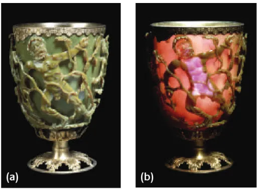
As shown in Figure 1-1, the glass appears red (a) when viewed with light transmitted through the cup, and green (b) when viewed with light reflected from the surface of the cup. This remarkable behavior is the result of the introduction of colloidal gold and silver into the glass during formation.
Ian Freestone 1 , Nigel Meeks 2 ,
Margaret Sax 2 and Catherine Higgitt 2
Introduction
Optical Properties of Materials
Here n is the ratio of the speed of light in vacuum to the speed of light in the material, and κ is the extinction coefficient of light within the material. This representation is more directly related to the experimental observation of light interacting with matter.
Metals
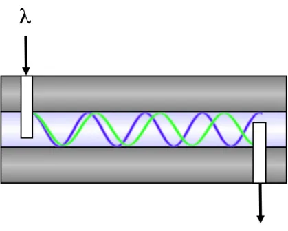
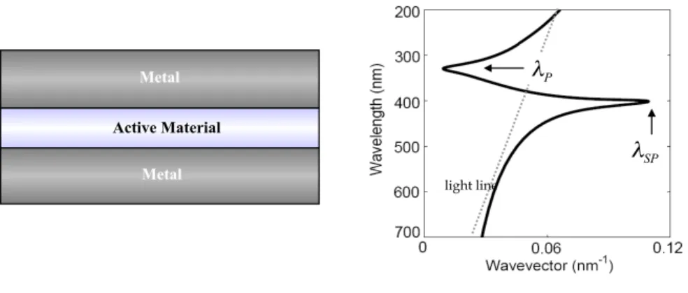
For both sets of equations, kx represents the component of the wave vector in the direction of propagation along the metal-dielectric interface. This plot shows the existence of the plasmonic mode as well as one photonic mode within the structure.
Scope of this Thesis
The figure on the left shows a generalized scheme of semi-infinite metal-insulator-metal waves. The idea is to take advantage of the electro-optical effect in ferroelectric materials and change the refractive index within the waves under an ap-.
Introduction
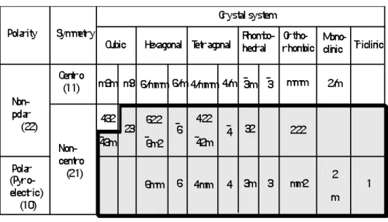
Point Groups and Crystal Symmetry
In the cubic state, the A atom lies in the center of the unit cell, the B atoms lie in the 8 corners, and the oxygen atoms lie in the 6 face-centered positions. As a result, above Tc, the Ba atom sits in the center of the cubic unit cell and is surrounded by the 4 oxygen atoms in the central plane of the unit cell.
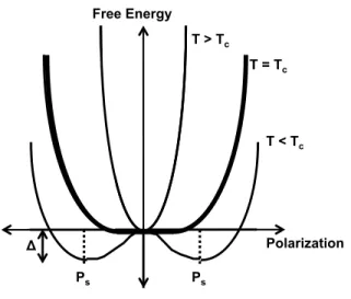
Landau-Ginsburg Theory of Ferroelectrics
For the case of the tetragonal unit cell of BaTiO3, this corresponds to ±Pz polarization. Here,±Pz can be seen below the x-axis and no spontaneous polarization can be seen in the curve representing T>Tc.
Electro-optic Effects
In the case of an electric field applied in the ˆz direction, the redistribution of the ions within the lattice will cause an elongation in the ˆz direction and a corresponding contraction in the ˆx and ˆy directions. As a result, the electron density (and index or refraction) will decrease in the ˆz direction and increase in the ˆx and ˆy directions.
Piezoresponse Force Microscopy
This is necessary because the piezoresponse signal from the sample is usually close to the lower detection limit of the AFM and as a result, the topography will dominate the output signal. This is especially true with rough samples which may also have surface oscillation frequencies which are similar to those of the piezo response.
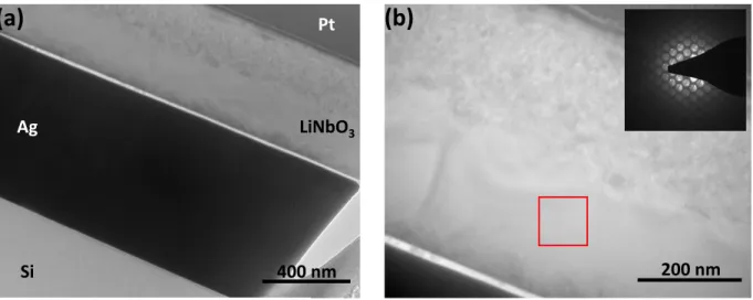
Ion Implantation Induced Layer Transfer
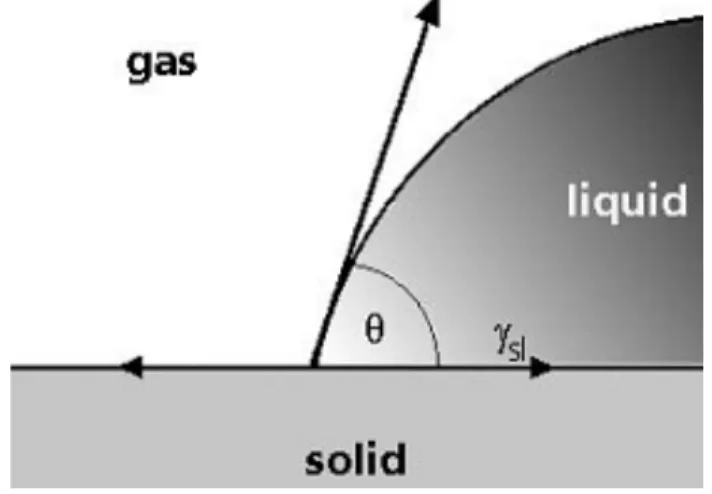
The effectiveness of the plasma activation can be determined using contact angle measurements of the “as treated” surface with a microsyringe imaging system, Figure 2.5. After the surface treatment of the implanted sample and the substrate is completed, the two surfaces are brought into contact under high temperature and pressure.

Introduction
Ferroelectric Materials
Integrating most of these technologies with conventional silicon-based device applications has proven difficult due to the high growth temperatures required and the need for an epitaxial template. Recently, progress has been made in the integration of single crystal ferroelectrics through the production of single crystal thin films.
Experimental Work
Analysis of the Layer Transfer Process
Phases that are thermodynamically unstable disappear in the search for the global Gibbs free energy minimum. In the piezoresponse image [Figure 3.8(c) and (f)], the bright and dark areas come from regions where the polarization vectors point in and out of the plane, respectively.
Conclusion
Local piezo response hysteresis curves compare PLD BaTiO3 on a Pt/Si substrate and low transferred BaTiO3 on Pt. Based on these results, the ion-implantation-induced layer transfer has been successfully used to create high-quality single-crystal ferroelectric thin films that can be bonded to substrates with significant thermal expansion mismatch.
Introduction
Layer Transfer and Lithium Niobate
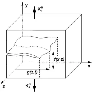
Geometry of the System and Stress State of the Film
The dashed plane coincides with the plane of ion implantation and the thickness of the transferred layer, h, corresponds to the depth of ion implantation. During the heating phase of the process, the film is subjected to a homogeneous biaxial stress σm caused by the mismatch in thermal expansion between the film and the substrate.

Stability of Microcracks in the Film
We will see that to ensure the transfer of a thin film without unwanted transverse cracks, the stress placed on the film must be within a certain range of values to be determined in Secs.
STABILITY OF MICROCRACKS IN THE FILM
- Buckling, Delamination, and Failure of the Film
In other words, the crack stability is mainly dictated by an expression proportional to dxdf, leading to the approximation:. The evolution of the local slope of the crack surface can be estimated from this equation.

Failure of the thin film induced by bending
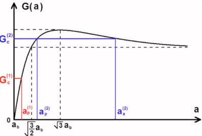
It is interesting to note that at the onset of film cracking 共 a = ab兲 there is no driving force for delamination 共 G = 0 兲. As a result, propagation is possible at a certain voltage level when the condition G 共 a 兲 = Gc is satisfied.
Comparisons of the various length scales of the problem and criterion for film failure
- Discussion and Comparison with Experimental Results
- DISCUSSION AND COMPARISON WITH EXPERIMENTAL RESULTS
In this representation, the state of the system at a given time corresponds to the point (|σm|,a). In both diagrams, the shaded zone corresponds to conditions of the system where the film is.
Effect of the compressive/tensile state of the stress on the stability of cracks
It is interesting to note that in the limit of very small errors a Ⰶ adel both types of systems, represented by two quite different diagrams, lead to the same expression for the critical compressive stress for film cracking. The first experiment is devoted to studying the stability of microcracks in
6 兲
Effect of a high compressive stress on the film The second experiment was performed on a system
- Conclusion
- Introduction
- Wafer Bonding Limitations
- Experimental Work
- Analysis of Silver Diffusion Bonding
- Conclusion
- Introduction
- Color Filtering and Plasmonics
- Metal-Insulator-Metal Color Filtering
It is now possible to identify the various processes that led to the failure of the film. This value is given by the intersection of the horizontal arrow with the curve ab.
Results from Passive Silicon Nitride Color Filtering
Experimental measurements of these structures showed color filtering across the red, green, and blue regions of the visible spectrum.
Blue!
Green!
Red!
Wavelength (nm)!
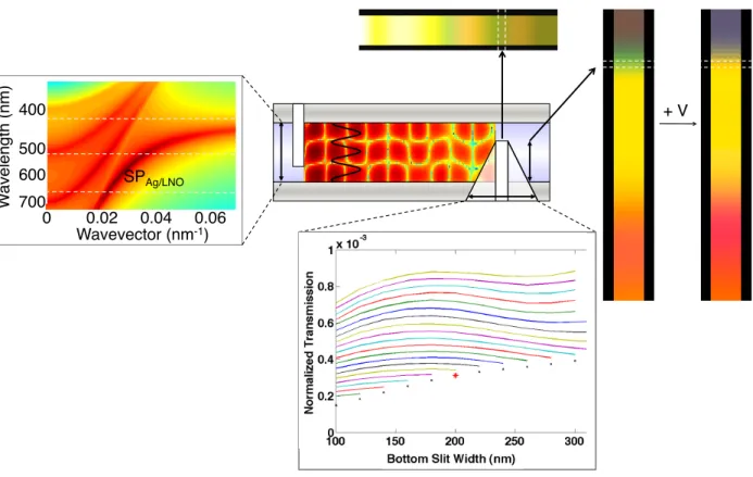
SP Ag/SiN/Au
Wavevector (nm -1 )!
Modeling Active Color Filters
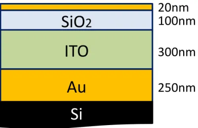
The structures used in the simulations had 400 nm of silver on the top and bottom of the waveguide with 300 nm of lithium niobate as the dielectric layer. Using spectroscopic ellipsometry, the complex refractive index of lithium niobate was measured and these data were used for all simulations.
3000 ! d sep (nm)!
V applied !
As a result, the dominant green oscillations seen in the upper color strip in Figure 6.7 are no longer present in the lower color strip.
V applied !V0!
Losses
For MIM waveguides where the dielectric thickness is below the cutoff for all the photonic-like modes, the only modes supported are the symmetric and anti-symmetric plasmon modes [71]. In this case, a significant amount of the electric field of these "bound" modes is located in the metal.
Increasing Slit Transmission
Even in these initial studies varying the shape and dimensions of the entrance and exit slits, Figures 6.11 and 6.12 show that the amount of light transmitted through these devices can be increased significantly (sometimes by at least an order of magnitude) with simple optimization. . For simplicity, all dimensions of the input and output slots were exactly the same in all simulations; however, future work will focus on independently varying these parameters to better optimize the devices for a given application.
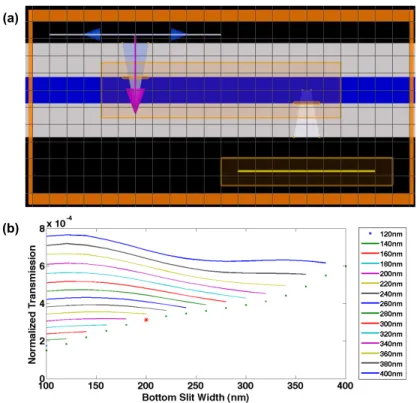
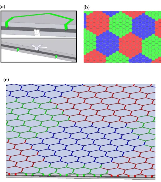
High Density Color Filtering Design
These structures could be designed so that the largest dimension is still smaller than the ~80 µm resolution limit of the human eye at 35 cm [18]. For a given 5 µm slit at a given wavelength within the superpixel structure, these devices provide between 0.02% and 0.1% transmission.
Conclusion
To maintain a uniform density of all three colours, the slit spacing can be kept constant across all devices and the different colors of each 'super pixel' can be selected simply by varying the depth of those pixels. The top panel shows half of the hexagonal output structure, while the bottom panel shows half of the three-slit input configuration for a given hexagon.
Introduction
CMOS and the Emergence of Plasmonics
Unfortunately, as gate lengths approach the single-nanometer scale, Moore's Law becomes increasingly difficult to follow. MOS scaling is accompanied by increased circuit delay and higher electronic power dissipation—a major impediment to Moore's Law, often referred to as the interconnect bottleneck.
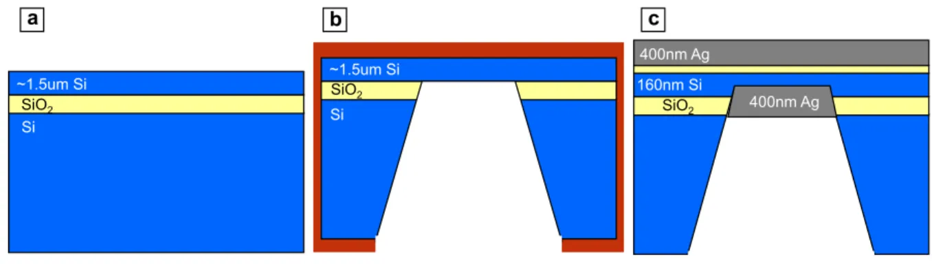
Design and Fabrication of the plasMOStor
After oxidation, 400 nm of silver was evaporated on the top and bottom surfaces of the membrane. The nearly flat dispersion of the photonic mode around λ= 1.55µm suggests that this mode will be extremely sensitive to changes in the Si complex index.
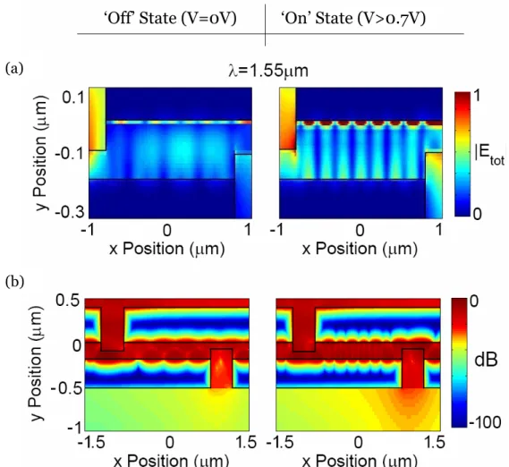
Switching Behavior
Finite difference time domain simulations of the plasmostor with λ = 1550 nm, showing the total electric field and transmitted power for a 2 µm long optical source-drain separation. Finite difference time domain simulations of the plasmostor with λ = 685 nm, showing the total electric field and transmitted power for a 2 µm long optical source-drain separation.
Time Response Analysis
Conclusion
Introduction
Carrier Modulation in Active Plasmonics
An alternative solution to this problem is to choose a dielectric material whose carrier density is much higher, and as a result, will have a plasma frequency closer to the visible and near-infrared frequencies of interest. As can be seen from the figure, working with carrier concentrations in the order of 1020−1021cm−3, the plasma frequency of the layer will stay in the near-infrared to visible frequency regime.
Fabrication and Characterization
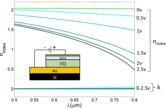
Films of InTiO3 were deposited on quartz slides and Hall probe measurements determined that the electron mobility in these films was µ= 14.5 cm2/V and the electron equilibrium concentration was n=5×1020 cm−3. As a result, we obtained n= 1×1020 cm−3, which agrees well with the value measured with the Hall probe.
Index Shifting in Indium Tin Oxide
It should be noted that further studies of the layered structure revealed a number of additional features indicating a shift of the plasma frequency by charge accumulation. Third, the same amount of peak shift was observed when the thickness of the InTiO3 layer increased or decreased, implying that there was no change in the accumulation layer.
Mode Modulation in Metal/InTiO 3 /Metal Waveguides
Complex refractive index is plotted as a function of wavelength and carrier concentration within the InTiO3 layer from n cm−3. First, this effect was not observed when a negative voltage was applied to the upper, semi-transparent electrode and there was no longer an accumulation layer at the InTiO3/SiO2 interface.
Conclusion
Representative one- and two-dimensional mode profiles are shown inside the waveguide cavity. Methods for modifying the production of MIM color filters included: changing the thickness (left); variation of exit slit depth with and without an applied electric field (right); change in separation between inlet and outlet slits (top); by changing the shape of the inlet and outlet slits (bottom).
Metal
In this appendix, we analyze the thin film dispersion relations for a metal-insulator-metal wave channel.1 Both transverse magnetic and transverse electric conditions will be considered.
Metal + d/2
- The General Solution
- Boundary Conditions
- Tensor Notation
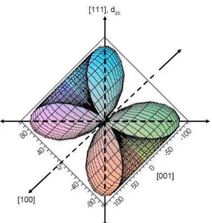
- Orientation Effects of Crystal Properties
Due to the fact that these tensors are symmetrical at a given polarization, we can reduce the number of elements in each layer of the tensor by half. Each layer in the film stack is represented mathematically by a suitable model that relates the thickness and dielectric constants of the material.
Wavelength (nm)
For lithium niobate with and without an applied electric field, the imaginary part of the refractive index was kept constant. Rodriguez, “Nanoscale investigation of the piezoelectric properties of perovskite ferroelectrics and iii-nitrides,” Ph.D.