ERIC BOGATIN
TO
AND
BOGATIN’S
PRACTICAL GUIDE PROTOTYPE
BREADBOARD
PCB DESIGN
BOGATIN’S PRACTICAL GUIDE to PROTOTYPE BREADBOARD and
PCB DESIGN
ERIC BOGATIN
E-ISBN: 978-1-63081-848-7 Cover design by Charlene Stevens
© 2021 Artech House 685 Canton Street Norwood, MA 02062
bogatin title.indd iii
bogatin title.indd iii 9/22/2021 11:50:44 AM9/22/2021 11:50:44 AM
3
Table of Contents
Chapter 1 A Getting-Started Guide ... 13
1.1 Who This Book Is For ... 14
1.2 Getting Stuff Done ... 16
1.3 Cost-Performance Trade-offs ... 18
1.4 Errors, Best Practices, and Habits ... 22
1.5 Learn to Design-in Success ... 25
1.6 A Getting-Started Guide for Signal Integrity ... 26
1.7 The Seven-Step Process ... 29
1.8 Risk Management and Mitigation ... 30
1.9 Two Risk Management Design Strategies... 32
1.10 Master of Murphy’s Law ... 33
1.11 Proof of Concept ... 35
1.12 Practice Questions ... 38
Chapter 2 PCB Technology ... 39
2.1 PCB, PWB, or PCA? ... 39
2.2 Physical Design of a PCB ... 40
2.3 Vias Technologies ... 41
2.4 Thermal and Thermal Relief Vias ... 45
2.5 Other Layers ... 48
2.6 The Soldermask Layer ... 49
2.7 Surface Finishes... 51
2.8 The Silk Screen ... 53
2.9 What the Fab Vendor Needs ... 54
2.10 Practice Questions ... 55
Chapter 3 Signal Integrity and Interconnects ... 57
3.1 Transparent Interconnects ... 58
3.2 When Interconnects are NOT Transparent ... 60
3.3 Where Signal Integrity Lives ... 65
3.4 Six Categories of Electrical Noise ... 71
3.5 Families of SI/PI/EMI Problems ... 74
3.6 In Principle and In Practice ... 76
3.7 Net Classes and Interconnect Problems ... 79
3.8 Design for Performance ... 82
3.9 Design for X ... 84
3.10 Practice Questions ... 85
Chapter 4 Electrical Properties of Interconnects ... 87
4.1 Ideal vs Real Circuit Elements ... 87
4.2 Equivalent Electrical Circuit Models ... 94
4.3 Parasitic Extraction of R, L, and C Elements ... 98
4.4 Describing Cross Talk ... 102
4.5 Estimating Mutual Inductance ... 105
4.6 Training Your Engineer’s Mind’s Eye ... 108
4.7 Electrically Long Interconnects... 109
4.8 Electrically Short and Electrically Long... 111
4.9 Practice Questions ... 119
Chapter 5 Trace Width Considerations: Max Current ... 121
5.1 Best design practices ... 122
5.2 Minimum Fabrication Trace Width ... 122
5.3 Copper Thickness as Ounces of Copper ... 123
5.4 Maximum Current Handling of a Trace ... 126
5.5 Maximum Current Through a Via ... 132
5.6 Thermal Runaway with Constant Current ... 133
5.7 Practice Questions ... 140
Chapter 6 Trace Width Considerations: Series Resistance ... 143
5
6.1 Resistance of Any Uniform Conductor... 143
6.2 Sheet Resistance of a Copper Layer ... 148
6.3 Measuring Very Low Resistances ... 152
6.4 Voltage Drop Across Traces ... 156
6.5 The Thevenin Model of a Voltage Source ... 157
6.6 How Much Trace Resistance Is too Much?... 165
6.7 The Resistance of a Via ... 167
6.8 Resistance of a Thermal Relief Via ... 172
6.9 Practice Questions ... 174
Chapter 7 The Seven Steps in Creating a PCB ... 177
7.1 Step 1: Plan of Record... 178
7.2 Step 2: Create the BOM ... 180
7.3 Step 3: Complete the Schematic ... 182
7.4 Step 4: Complete the Layout, Order the Parts ... 183
7.5 Steps 5 and 6: Assembly and Bring-Up ... 185
7.6 Step 7: Documentation ... 187
7.7 Practice Questions ... 189
Chapter 8 Step 1, POR: Risk Mitigation ... 191
8.1 Visualize the Entire Project Before You Begin ... 191
8.2 Avoid Feature Creep ... 193
8.3 Estimate Everything You Can... 193
8.4 Preliminary BOM: Critical Components ... 195
8.5 Risk Assessment ... 195
8.6 Risk Mitigation: Tented Vias ... 198
8.7 Risk Mitigation: Qualified Parts ... 202
8.8 Practice Questions ... 204
Chapter 9 Risk Reduction: Datasheets, Reverse Engineering, and Component Selection ... 207
9.1 Take Responsibility for Your Design ... 207
9.2 Reducing the Risk of a Design Problem... 208
9.3 Understand Your Circuit ... 209
9.4 Read Datasheets Critically ... 212
9.5 Build Simple Evaluation Prototypes ... 212
9.6 Reverse Engineer Components ... 213
9.7 Reuse Parts ... 216
9.8 Practice Questions ... 218
Chapter 10 Risk Reduction: Virtual and Real Prototypes ... 221
10.1 Getting Started with Circuit Simulation ... 221
10.2 Practice Safe Simulation ... 225
10.3 Simulating a 555 Circuit ... 227
10.4 Purchase an Evaluation Board ... 231
10.5 Real Prototypes with Modules ... 231
10.6 Practice Questions ... 233
Chapter 11 Risk Reduction: Prototyping with a Solderless Breadboard .... 235
11.1 Build a Real Prototype... 236
11.2 Solderless Breadboards for POC ... 238
11.3 Features of a Solderless Breadboard ... 239
11.4 Bandwidth Limitations ... 244
11.5 A Simple Breakout Board ... 251
11.6 The Mini Solderless Breadboard ... 254
11.7 Best Wiring Habits ... 255
11.8 Habit #1: Consistent Column Assignments ... 256
11.9 Habit #2: Color Code the Wires ... 259
11.10 Habit #3: Keep Signal Traces Short ... 260
11.11 Habit #4: Avoid a Shared Return Path... 263
11.12 Habit #5: Route Signal-Return Pairs ... 263
7
11.13 Habit #6: Keep Component Leads Short ... 266
11.14 Practice Questions ... 267
Chapter 12 Switching Noise and Return Path Routing... 269
12.1 The Origin of Switching Noise ... 271
12.2 Signal-Return Path Loops... 274
12.3 Where Does Return Current Flow? ... 279
12.4 A Plane as a Return Path... 283
12.5 Ground ... 287
12.6 Avoid Gaps in the Return Plane... 290
12.7 Summary of the Best design practices... 292
12.8 Practice Questions ... 293
Chapter 13 Power Delivery ... 295
13.1 Origin of Power Rail Switching Noise ... 295
13.2 Calculating Loop Inductance ... 298
13.3 Measuring PDN Switching Noise ... 300
13.4 The Role of Decoupling Capacitors ... 302
13.5 Where Do Decoupling Capacitors Go? ... 305
13.6 The Power Delivery Path ... 309
13.7 Inrush Current ... 311
13.8 Summary of the Eight Habits for Using a SSB ... 312
13.9 Practice Questions ... 313
Chapter 14 Design for Performance: The PDN on a PCB ... 315
14.1 VRM specifications ... 316
14.2 Voltage Regulator Module ... 317
14.3 Self- and Mutual-Aggression Noise ... 319
14.4 Power and Ground Loop Inductance ... 320
14.5 Decoupling Capacitors ... 323
14.6 A Decoupling Capacitor Myth; Part 1... 326
14.7 A Decoupling Capacitor Myth; Part 2 ... 330
14.8 Routing for Power Distribution ... 335
14.9 Ferrite Beads ... 336
14.10 Summary of the Best design practices ... 343
14.11 Practice Questions ... 344
Chapter 15 Risk Reduction: Design for Bring-Up ... 347
15.1 Test is Too General a Term ... 347
15.2 What Does It Mean to “Work”? ... 351
15.3 Design for Bring-Up ... 353
15.4 Add Design for Bring-Up Features ... 355
15.5 Jumper Switches ... 358
15.6 LED indicators ... 359
15.7 Test Points ... 361
15.8 The Power Rail as a Diagnostic ... 366
15.9 Practice Questions ... 371
Chapter 16 Risk Reduction: Design Reviews ... 373
16.1 The Preliminary Design Review ... 373
16.2 The Critical Design Review ... 374
16.3 DRC for DFM in the CDR ... 378
16.4 DRC for Signal Integrity ... 378
16.5 Layout Review ... 379
16.6 Practice Questions ... 381
Chapter 17 Step 2: Surface-Mount or Through-Hole Parts ... 383
17.1 Through-Hole and Surface-Mount ... 383
17.2 Types of SMT Parts ... 385
17.3 Integrated Circuit Components ... 388
17.4 Practice Questions ... 393
Chapter 18 Finding the One Part in a Million ... 395
9
18.1 An Important Selection Process ... 395
18.2 Trade-offs in Selecting Parts ... 397
18.3 The Search Order to Select a Part ... 398
18.4 Selecting Resistors ... 402
18.5 Selecting Capacitors ... 405
18.6 The BOM ... 408
18.7 Summary of the Best design practices... 409
18.8 Selecting Parts for Automated Assembly ... 411
18.9 Practice Questions ... 412
Chapter 19 Step 3: Schematic Capture and Final BOM ... 413
19.1 Picking a Project Name ... 414
19.2 Schematic Capture ... 416
19.3 Take Ownership of Reference Designs ... 417
19.4 Add Options to Your Schematic ... 418
19.5 Best design practices for Schematic Entry... 418
19.6 Design Review and ERC... 423
19.7 Practice Questions ... 424
Chapter 20 Step 4: Layout — Setting Up the Board ... 425
20.1 Layout ... 425
20.2 Board Dimensions ... 426
20.3 The Layers in a Board Stack ... 428
20.4 Negative and Positive Layers ... 428
20.5 Examples of Some Fab Shop DFM Features ... 430
20.6 Setting Up Design Constraints ... 432
20.7 Thermal Reliefs in Pads and Vias ... 433
20.8 Set Up Board Size and Keepout Layer ... 436
20.9 Practice Questions ... 437
Chapter 21 Floor Planning and Routing Priority ... 439
21.1 Part Placement ... 439
21.2 The Order of Placement and Routing ... 442
21.3 First Priority: Ground Plane on the Bottom Layer ... 443
21.4 Second Priority: Decoupling Capacitors ... 445
21.5 Third Priority: Ground Connections ... 446
21.6 Fourth Priority: Digital Signals, Congested Signals ... 447
21.7 Fifth Priority: Power Paths ... 449
21.8 The Silk Screen ... 451
21.9 Check the Soldermask ... 453
21.10 Soldermask Color ... 454
21.11 Layout — Critical Design Review ... 455
21.12 Practice Questions ... 458
Chapter 22 Six Common Misconceptions about Routing ... 459
22.1 Myth #1: Avoid 90 Deg Corners ... 459
22.2 Myth #2: Add Copper Pour on Signal Layers ... 461
22.3 Myth #3: Use Different Value Decoupling Capacitors... 465
22.4 Myth #4: Split Ground Planes ... 465
22.5 Myth #5: Use Power Planes ... 466
22.6 Myth #6: Use 50 Ohm Impedance Traces ... 467
22.7 Practice Questions ... 470
Chapter 23 Four-Layer Boards... 473
23.1 Two-Layer Stack-Ups ... 473
23.2 A 4-Layer Board ... 474
23.3 Four-Layer Stack-Up Options ... 476
23.4 Stack-Up Options with Two Planes ... 478
23.5 The Recommended 4-Layer Stack-Up ... 480
23.6 When Signals Change Return Planes... 481
23.7 Practice Questions ... 483
11
Chapter 24 Release the Board to the Fab Shop ... 485
24.1 Gerber Files ... 485
24.2 Cost Adders ... 486
24.3 Board Release Checklist ... 488
24.4 Practice Questions ... 489
Chapter 25 Step 6: Bring-Up ... 491
25.1 Does Your Widget Work? ... 491
25.2 Prototype or Production Testing ... 492
25.3 Design for Bring-up ... 494
25.4 Find the Root Cause ... 495
25.5 Problems to Expect ... 497
25.6 Troubleshoot Like a Detective ... 500
25.7 Trick #1: Recreate the Problem ... 502
25.8 Trick #2: Seen This Problem Before? ... 503
25.9 Trick #3: Round Up the Usual Suspects ... 504
25.10 Trick #4: Three Possible Explanations ... 505
25.11 A Methodology... 506
25.12 Forensic Analysis ... 507
25.13 Coding Issues ... 512
25.14 Practice Questions ... 513
Chapter 26 Step 7: Documentation ... 515
Chapter 27 Concluding Comments ... 517
Chapter 28 About Eric Bogatin ... 519
12
Dedication
This book is dedicated to my wife, Susan. Her constant encouragement and support made this book possible.
13
Chapter 1
A Getting-Started Guide
Printed circuit boards range in complexity from a simple 1-layer board with a few components and nets, to a 32-layer or more board with thousands of components and tens of thousands of nets. This range is illustrated in Figure 1.1.
Figure 1.1 An example of the range of circuit board complexity. Left: a simple 1-layer board, courtesy of Altium and right: a complex server board, courtesy of Intel.
In designing, fabricating, and bringing to life these boards, there are some basic techniques we will use for both the simplest and the most complex boards and there are some techniques we will need only for the most complex boards.
This book is really a getting started guide in the basic techniques we will use over and over again for all circuit boards. We limit the scope of this book to simpler, 2-4-layer designs that can generally be purchased for the lowest prices on internet PCB fab sites and assembled remotely using captive assembly lines with limited, captive parts stockrooms.
When a completely assembled, fully custom board can be purchased for less than $10 a board in quantities of two, these skills will enable
a hobbyist, a maker, a student, or a young engineer to accelerate up the learning curve as an experienced hardware engineer.
1.1 Who This Book Is For
This book is for the casual user, not the power user. We focus primarily on the outcome of the design process, and only a little on the specific mouse clicks or menu items to implement the outcome, which will vary from electronic design automation (EDA) tool to EDA tool.
For example, when placing a via to route a signal from one layer to another, there are multiple methods. Regardless of the tool, unless you have a strong compelling reason otherwise, you should always use a via with the smallest drill diameter your fab vendor can implement with no cost adder.
In a 4-layer board, a return via should be added adjacent to the signal via if the return plane changes.
These are design principles you will learn to implement as a good habit to reduce noise. What you should implement in your designs as good habits is the focus of this book; how you implement the features using your favorite EDA tool is still very important as a designer but is not the focus of this book.
The methods we introduce in this book can be implemented with the range of EDA PCB design tools, from the free online internet tools to the high-end professional tools.
If you are looking for a tool to use, there are generally two classes:
simple and free, and professional level and not free.
Simple, low-end, free tools:
✓ Circuit Maker, from Altium: https://circuitmaker.com/
✓ Fritzing: https://fritzing.org/
✓ Easyeda: https://easyeda.com/editor
1.1 Who This Book Is For 15
✓ DesignSpark: https://www.rs- online.com/designspark/home
✓ PCB123, from Sunstone: https://www.sunstone.com/pcb- resources/cad-tools/pcb123
Professional-level tools for engineers:
✓ KiCAD: https://kicad.org/ (free)
✓ Eagle from Autodesk:
https://www.autodesk.com/products/eagle/overview?plc=
F360&term=1-YEAR&support=ADVANCED&quantity=1
✓ Altium Designer: https://www.altium.com/
✓ Siemens PADS Pro: https://www.pads.com/
✓ Cadence Allegro:
https://www.cadence.com/en_US/home/tools/pcb-design- and-analysis/pcb-layout/allegro-pcb-designer.html
Whichever tool you use, learn the basic steps to capture a schematic and design a board layout. The more you use the tool, the farther up the learning curve you will want to advance to become more efficient with your chosen tool.
There are some limitations to the type of designs we cover in this book. We assume all the routing can be implemented in an up to 4- layer board using at most two signal layers. This means the
challenges of ball grid array (BGA) parts are not covered in this book.
These components require a whole new set of design and layout principles because of the higher interconnect densities required.
If you deal with BGA parts, you will want to check out the book by Charles Pfeil, BGA Breakouts And Routing: Effective Design Methods For Very Large BGAs, available here, for example:
https://www.amazon.com/BGA-Breakouts-Routing-Effective- Methods/dp/1452867585
While the examples in this book are implemented as 2- and 4-layer boards, the driving forces for the guidelines and habits
recommended will apply across the spectrum of boards.
The most basic electrical considerations and analysis for current handling, return path control, power rail decoupling, and ground bounce reduction are introduced and will transcend all designs.
The principles underlying the design guidelines to reduce electrical noise are extensively included so that every designer will be empowered to make their own decisions when trading off design features with acceptable noise, cost, schedule, and risk.
The habits introduced in this book will apply from DC to very high frequency, but they are not enough.
We limit the electrical considerations to those interconnects that are electrically short: transmission line behavior does not apply,
interconnects do not require termination strategies, and the routing topologies do not affect signal quality. These are very important considerations when interconnects are electrically long and this topic is covered in detail in another book in this series, Bogatin’s Practical Guide to Transmission Line Design and Characterization for Signal Integrity Applications, published by Artech in May 2020.
A functioning circuit board is more than just a bare printed circuit board. It also includes the component selection, circuit design, assembly and bring-up, test, and characterization. These topics, especially when the lowest cost is an important driving force, are covered extensively in this book.
1.2 Getting Stuff Done
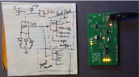
This book focuses on GSD (getting s#!t done). It is a practical, how- to, soup-to-nuts book on how to take a back of the napkin (BoN) sketch and turn it into a working widget prototype. An example is shown in Figure 1.2.
1.2 Getting Stuff Done 17
Figure 1.2 An example of a back of the napkin (BoN) sketch for a concept and the working widget prototype from this concept, built by one of my students.
This book introduces a seven-step process for prototype development. Once the prototype has been verified, there is a
different development track to turn this prototype into a production- ready product and then go through qualification testing, certification testing, ramping up volume production, and cost reductions.
The production ramp path is outside the scope of this book.
The purpose of this book is to increase your success at turning a BoN sketch into a working widget prototype when a printed circuit board is required as the backbone platform to interconnect all your
components.
More importantly, it is about developing good design and
measurement habits, which will increase your chance of success in all of your projects and position your circuit board projects for production. You will use these habits over and over again, for all of your designs. Hopefully, you will teach others these good habits so that your team will have an increased chance of success as well.
1.3 Cost-Performance Trade-offs
The most important goal in product design, which influences all decisions you make, is to achieve a target performance (provide value to the final customer) at an acceptable price to the final user and at an acceptable cost to produce.
When profit is important, the goal is maximum value to the customer and profit to the company. When profit is not important, such as building a prototype for internal use, the goal is maximum value at an acceptable cost.
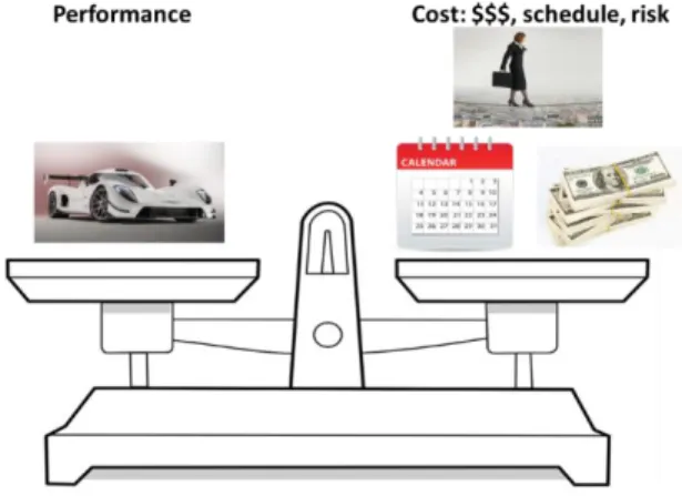
In the development phase, the cost is not just the final cost to manufacture the product. It also includes the development costs in terms of cash, schedule, and risk. This fundamental trade-off is illustrated in Figure 1.3.
Figure 1.3 The fundamental trade-offs between performance and the three different costs in the development phase.
Sometimes it is worth it to pay more for a component if it reduces the total cost of ownership (TCOO). For example, using an integrated switch mode power supply (SMPS) may be more expensive than the discrete solution with multiple resistors, capacitors, and inductors, but the integrated solution may reduce assembly cost and risk. This is part of the trade-off decision.
1.3 Cost-Performance Trade-offs 19
Sometimes, it is worth adding a higher cost feature if it gives your product higher value. Adding a Bluetooth interface may enable your product to be controlled by a smart phone. If the extra cost adds enough value to cover this cost and some profit, it has a favorable return on investment (ROI). This is part of the trade-off decision.
Rarely is it possible to add value to the product and not increase one of the cost metrics. When you can increase value with little cost adder, it’s a no-brainer. Make the decision, as long as there is no strong compelling reason otherwise.
Using a soldermask color on your circuit board that adds brand recognition to your product, like the purple of Adafruit or the red of Sparkfun, is a no-brainer.
Increasing the temperature resolution on a display from 0.1 deg to 0.01 deg at the cost of a $1.05, 16-bit ADS1115 ADC may not be worth the value returned for an ambient room temperature sensor, but may be well worth it for a health monitor temperature sensor.
Rarely is it possible to reduce one of the cost metrics without increasing one of the other metrics. Using six layers for your circuit board may reduce the risk of a noise problem but will increase the dollar cost budget.
In the product definition stage, this trade-off is sometimes referred to as the triple constraint between:
✓ Cost
✓ Time
✓ Scope (features or value)
Once the product is defined, in the product development phase, this is referred to as the constraint triangle:
✓ Lowest cost
✓ Highest quality
✓ Done quickly
You can have any two, but not all three at the same time.
The product development process is really about balancing these sorts of trade-offs.
There is an important, explicit element missing from these analyses that applies specifically to new product development and prototypes in particular: the risk of not being successful.
The element of risk is buried in the quality statement but should be explicitly brought out and addressed. Whenever you are doing something new that has not been done before, in exactly the way you are doing it, there is always the element of risk:
✓ Will the components you select work the way you expect?
✓ Will the circuit schematic be correct?
✓ Will you be able to create the code needed?
✓ Will the circuit board footprints match the pads of your components?
✓ Will your board come back from the vendor on the schedule you expect?
✓ Will the noise created by the circuit board be low enough to not interfere with the operation of the circuit?
Risk reduction rarely comes for free. Paying more dollars for features to reduce noise will reduce risk or reduce the time if it means no second board spin. Sometimes, it is worth paying more for reduced risk and reduced time. This is called buying insurance.
If you reduce the dollar cost, you may increase the risk of the product not working initially (the quality) or over the product lifetime (the reliability). If you buy a lower-cost row of header pins from a new vendor and it breaks too easily, it may not be worth the cost reduction. This is why it is important to qualify a part and a vendor before you commit to it. This is part of risk reduction.
If you reduce the schedule, you may have to increase the risk and increase the dollar cost. If you do not want to take the time for a qualification test of a new part, you can pay more for an unqualified
1.3 Cost-Performance Trade-offs 21
part from a qualified vendor, or use an unqualified part in stock rather than wait for your qualified part.
If you can make a design decision that reduces the risk without impacting performance or value, at the same or lower cost or schedule, it’s a no-brainer. We call these decisions, best design practices.
A best design practice is a decision you make that reduces risk, or reduces cost or development time, with a favorable return on investment. Always follow a BDP unless you have
a strong compelling reason otherwise.
A little upfront planning to avoid common risks can have a large impact on success, and a favorable ROI. This is a best design practice.
Using a ground plane on the bottom layer of a circuit board will reduce some sources of noise. If you can fit all or most of your interconnects on the top layer, using the bottom layer for a
continuous ground has a favorable ROI. This is a best design practice.
Using silk screen labels to clearly identify the test points on your board for the 5 V rail, the clock output, and the three critical signals, does not add cost but will reduce the time for bring-up and the risk of measuring the wrong signal. It is a no-brainer and has a favorable ROI. This is a best design practice.
When it costs more if you follow a best design practice, it’s time to bring out your engineer’s hat and sharpened pencil and paper and do a cost-performance trade-off analysis. This usually involves
estimating the impact on performance, risk, cost, and schedule using rules of thumb, approximations, or numerical simulations.
Using a more expensive capacitor rated for 200 V will be more reliable than a similar-value, lower-cost capacitor, but rated at only 25 V. But if the application is for a 5 V rail, the lower reliability risk offers no additional value so this decision may not be a favorable ROI.
In some companies, historical events affect what is perceived as acceptable risk. If a significant problem resulted in a previous product’s delayed introduction to the market, the fix may be
required for all future product, whether it is needed or not. This is an emotional response to an engineering trade-off.
If a ceramic resonator was used as a clock reference and it resulted in a batch of microcontroller boards that did not boot because the resonator did not oscillate, the corporate culture may ban ceramic resonators in favor of only quartz crystal resonators. This may be in spite of the fact that the resonator circuit just needed a shunt resistor to self-start. Once burned by a costly mistake, management has a tendency to overcorrect in future designs, independent of what is a good engineering decision.
1.4 Errors, Best Practices, and Habits
There are many decisions you will make when designing a
prototype. Should I use a 2-layer board or a 4-layer board? Will this low drop out (LDO) 3.3 V regulator work in my application? Should I use a 0.1 uF and 10 uF capacitor on my 5 V rail or a 22 uF capacitor?
Should I use the letters “TP1” for the silk screen label for a test point, or “5V rail” as the label?
There are many more ways of designing a product that fails than designing one that works. Navigating the decision tree and balancing all the trade-offs when designing and building your prototype is what engineering is all about.
There are generally two types of errors you can make that result in some form of reduced value or increased cost:
✓ Hard errors: the product does not work
✓ Soft errors: the product works, but the cost or noise (risk) may be higher than it could be
Sometimes, there are multiple ways of implementing a feature that will have a neutral impact on value or cost. The decision choice is a
1.4 Errors, Best Practices, and Habits 23
personal preference. These are not errors, but more about style. You choose which path to take.
Some decisions you make will result in a hard error. Your prototype will not work due to this problem. Using a 6 mil wide trace to route 10 A of current to a motor will result in a catastrophic failure when the trace melts or catches fire. This would be a hard error. Forgetting to connect a ground connection to an input power jack will result in your board not being powered when plugged in. This is a hard error.
Routing the TX from the controller to the TX pin of the UART driver will cause the communications link to fail. This is a hard error.
The other technical term for a hard error is, “you’re screwed.”
Some decisions you make will be neutral. Your product will probably work in spite of your decisions. If you had the chance to do it
differently next time, you would change your decision. This is a soft error.
Routing a long trace in the bottom ground layer may increase the ground bounce noise in your design, but it may still work, in this board, just fine. This is a higher risk and should be avoided next time.
The decoupling capacitor is placed an inch away from the power pin it is decoupling. It will probably work in this design, but there may be some combinations of microcode and functions where a bit error occurs. This is very hard to diagnose. It is a soft error and should be avoided in the future.
Not including a test point for the 5 V power rail will make the debugging more difficult, but the product will probably still work.
This will increase the risk and make it harder to debug your board. It is a soft error.
Labeling a test point as TP31 means you have to spend the time looking up what signal is at this test point. Next time, you would label this as 555 output, for example. This is a soft error.
Not adding your name or board ID to the silk screen is inconvenient, especially if you have ten different board designs you are exploring on your lab bench. The chance of getting them confused is high. Next
time you would add a unique board identifier in silk screen. This is a soft error. Of course, if it means not getting your board back from the general pool of boards, it could be a hard error.
Eliminating the hard errors and reducing the soft errors that may creep into your design is about reducing risk. An important process for reducing the risk of an error is by following best design practices.
There are so many little mistakes that are easy miss in a design, any of which could be either a hard or soft error. An important best design practice to minimize the chance of a mistake not being caught before the product is released to fab is to keep a checklist of possible problems. Many checklists are provided in this book. Start with these and add your own mistakes to the list. We will leverage the phrase over and over again.
An expert is someone who has made all the mistakes possible.
However, it is not necessary for you personally to make all the mistakes possible. Learn from the mistakes others have made.
Generally, we will try to use best design practices that can be leveraged across many designs and many applications. Learning them once, you will use them over and over again. If they are free and do not come at additional cost, they should become habits.
For example, an important best design practice is to use a continuous ground plane on the layer adjacent to signal layers. This best design practice will reduce the risk of ground bounce noise, a type of cross talk and a type of switching noise, which is often a source of
unexpected product failure.
Another best design practice is to use net names on all wires using a labeling scheme that groups similar nets in order when listed alphabetically. This simple best design practice reduces the risk of forgetting a connection or making the wrong connections when doing the board layout.
1.5 Learn to Design-in Success 25
Another best design practice is to use the minimum line width your fab shop can fabricate in order to increase your routing interconnect density without adding costs. Keep in mind, a 6 mil wide trace can handle as much as 1 A of current.
If the best design practice has a favorable ROI and is free, it is something you should always do, unless you have a strong compelling reason otherwise. We call these habits.
A habit is something you do without thinking. It comes
automatically. And it will increase your chance of success with little cost impact.
When the best design practice becomes a habit, you will be a more effective engineer. Teach these habits to the rest of your team and you will collectively become a more effective team. But recognize their origin so you can evaluate when you may have a strong compelling reason to not follow the habit.
1.5 Learn to Design-in Success
The traditional approach of prototype development is to “build it and test it.” When it doesn’t work, try to figure out why, and usually before you can find all the problems, the pressure is on to redesign it, build it again, test it, and see how far you can get.
Sometimes, this approach is called “testing-in success.” This
approach is way too inefficient. It takes too long, costs too much, and does not guarantee success.
The alternative is to plan to get it right the first time. And when you don’t get it right the first time, have a strategy to get it right the second time.
Spending an extra day in the planning phase may save you weeks to complete a new board design-spin, even assuming
you were able to find the actual design features to change to get it right in the next release.
It is in the planning phase that you should anticipate as many of the potential problems that can arise and put in place a plan to avoid each one. This is where your checklist of common mistakes made by others and which you have made is a valuable mechanism to not repeat them.
Use every mistake you make to ratchet up the learning curve so you never repeat it.
Before this book, your product development strategy should have been: design and execute the product as well as you can, but
anticipate there will be problems and unknowns, so plan to fail early and fail often and learn from your mistakes.
Following the guidelines in this book, your product development strategy should be fail less, succeed more.
This book introduces an efficient process to integrate best design practices to get it right the first time and best measurement practices to get it right the second time.
1.6 A Getting-Started Guide for Signal Integrity
This book is a getting-started manual for any engineering student or professional engineer to develop good design and measurement habits when designing and building electronic prototypes.
The schematic describes all of the components used in a design and how they are connected. On each component, like a resistor,
capacitor, LED, connector, op-amp, transistor, or other IC are connection points or terminals or pins or nodes. These are the features of each component electrically connected to other components.
All of this information about the components and their terminals is contained in a database for the bill of materials (BOM).
1.6 A Getting-Started Guide for Signal Integrity 27
All terminals that are connected together are connected by one specific net. The list of all the nets and what terminals are connected to each net is called the net list. This is the second important
database that really defines a design.
In a sense, the schematic is a graphical representation of the BOM and the net list databases. In most electronic design automation (EDA) tools, we manipulate the BOM and net list databases through a graphical user interface, the schematic capture tool.
The connections between the terminals of each component in a schematic are meant to only represent connectivity. They have no electrical properties other than an assumed 0 ohm connection. They say nothing about electrical performance.
It is when the schematic is translated into the physical interconnects of traces of copper that the electrical properties of the copper wires will play a role. All of the real, physical conductor (and insulating) structures that actually perform the electrical connections are considered the interconnects. All the cables, connectors, and any other conductors included in the connection paths from terminal to terminal, are considered the interconnects. Even the dielectrics that provide isolation between conductors are part of the interconnects.
When interconnects are electrically transparent, the interconnects’
only purpose is to provide connectivity between the terminals of all the components in the product. This is the case in both prototype solderless breadboard circuits and prototype printed circuit boards.
Once connectivity is established, the interconnects can only increase the electrical noise. Being transparent means the noise generated is acceptable for that design. But as rise times decrease and signals become more sensitive to noise, even in many common, low-cost designs, the interconnects may no longer be transparent. Their impact on signal quality must be taken into account in the design phase or your product may not work.
To evaluate when interconnects are no longer transparent, the very first step is to translate the physical properties of the interconnects, and their geometry and material properties, into their equivalent electrical circuit elements. Since the impact from these circuit
elements is only to “eat design margin” and “degrade performance,”
the equivalent electrical circuit elements of the interconnects are sometimes referred to as the parasitics of the interconnects.
Based on the equivalent circuit models of the interconnects, we can use rules of thumb, simple estimates, and numerical simulations to anticipate or predict the impact on noise from the interconnect design. Knowing the types of problems that can arise, we can establish a set of best design practices that will decrease the noise generated by the parasitics.
The process of translating the physical interconnects into their parasites, analyzing the impact from these parasitics, establishing design practices to reduce their impact, and the best measurement practices to measure these effects is all encompassed by the term signal integrity.
This book establishes the essential principles to get started with signal integrity and the best practices to mitigate these
effects to end up with an acceptable design.
This book covers the five important areas:
✓ Essential principles at the foundations of signal integrity
✓ How to translate physical interconnects into equivalent electrical circuit elements (parasitic extraction)
✓ How to estimate the impact on noise from the parasitics
✓ Best design practices for acceptable signal integrity
✓ Best measurement practices for signal integrity If you have been designing interconnects assuming they are transparent, this book will recalibrate your thinking to view interconnects as electrical circuit elements.
If you have been following design guidelines handed down from generation to generation, you will see some of the origins of these recommendations and make your own judgment as to when they apply and when they don’t.
1.7 The Seven-Step Process 29
With the principles introduced in this book, you will be empowered to be your own expert.
However, this book is just a getting-started guide. There are many more advanced signal integrity principles and best design and measurement principles to consider for ever-higher-speed products.
The principles described in this book are at the foundation of everything else you will want to do in every future higher- performance product.
Even if, in your current design, the interconnects are transparent, the habits you learn for good signal integrity design will position you for your next product where the interconnects may not be transparent.
When the best design and measurement practices become habits, it is more likely you will implement them in all of your designs and increase the chance of success in all of your future product designs.
1.7 The Seven-Step Process
Every new project starts with the product concept and the rough functional or block diagram or schematic that could be sketched on a napkin. In almost every case, we turn this concept into a working prototype circuit board by following these 7 steps:
1. Complete the plan of record (POR).
2. Complete the preliminary bill of materials (BOM).
3. Complete the final schematic capture and final BOM.
4. Complete the board layout and order all the parts.
5. Complete the assembly.
6. Complete the bring up, troubleshoot, and final test.
7. Complete the documentation.
These steps are defined by their outcomes or completions. These are milestones, distinct from tasks. A task is the process you go through while you are taking action. A milestone is the point at which you
have completed the task. Each step in the seven-step process is a task that ends in a milestone, the completion of the task.
When describing any plan, it is important to always pay attention to the difference between a milestone, which is a specific
accomplishment that has been completed, and a task which is an activity in which you are engaged.
A milestone is “the schematic is completed.” A task is “create the schematic.”
1.8 Risk Management and Mitigation
The goal of any design project is to create a product that meets the performance goals at an acceptable cost, risk, and schedule.
There are often only a few right ways of completing a design on time and on budget, but many, many wrong ways which go over budget and over schedule.
Much of the design and implementation process is about navigating safe passage along the narrow path winding through the product development forest. One step off the correct path and your product may fall off the edge of a cliff into disaster, such as in Figure 1.4.
1.8 Risk Management and Mitigation 31
Figure 1.4. An example of a disaster: the Montparnasse derailment of 1895. Source is Wikipedia.
The plan of record (POR) should anticipate as many as possible of these potential problems which could cause your product to not work. For each problem or risk, a plan should be created to reduce or mitigate this risk. The combination of identifying potential risks and planning to reduce them is risk management.
Much of this book focuses on risk reduction strategies. We will anticipate the potential risk sites and create a mitigation plan to reduce these foreseeable, potential problems.
The basic approach we will take is:
Design more like Ralphie’s Mom and less like a Colorado Bro.
1.9 Two Risk Management Design Strategies
There are two extreme approaches to risk management, which describe how to assess the risks in any endeavor. At the one extreme of thinking of every possible worst-case scenario is Ralphie’s mom, in the 1983 movie, A Christmas Story. At the other extreme of not being concerned about any risk is a “Colorado Bro.”
Ralphie’s mom would always think of the worst-case scenarios, all the things that could go wrong, such as, “Be careful, you could put your eye out with that,” referring to the possible consequences of using a BB gun.
A “Colorado Bro,” a colloquial description of a young, risk-taking snowboarder, is less worried about what could go wrong and more interested in the thrill of “let’s try it and see.”
When a Colorado Bro encounters an opportunity to take a risky path, we have an expression in Colorado that, rather than being cautious, Coloradans will sometimes say, “Here, hold my beer.”
These two approaches to life are illustrated in Figure 1.5.
Figure 1.5. Two design perspectives. Left: Design like Ralphie’s mom: think of all the worst-case scenarios and avoid what you can. Right: A Colorado Bro’s perspective is not
afraid of taking on risk, “Here, hold my beer.”
Designing more like Ralphie’s mom means think of all the things that can go wrong, anticipate them, avoid them, or plan a risk reduction strategy. After all, the goal is first-time product success, on time, and within budget. A risk site is a feature or event that may prevent you from reaching your goal.
1.10 Master of Murphy’s Law 33
1.10 Master of Murphy’s Law
Murphy’s Law, as we use it today, is “If something can go wrong, it will.” It was actually introduced by Captain Edward Murphy in 1949, shown in Figure 1.6. He was the lead engineer in the Air Force MX981 rocket sled project.
Figure 1.6 Air Force Captain Ed Murphy, the creator of Murphy’s law, in 1949, source is Wikipedia.
This rocket sled was testing the impact on test pilots from the high G acceleration and deceleration they would experience in soon-to-be- introduced high-performance jet aircraft.
As part of the experiment, a test pilot was strapped onto a rocket sled on a railroad track, instrumented with sensors for G-forces, temperature, heart rate, blood pressure, and other physiological signals. These signals were routed to a tape recorder on the rocket sled.
After one particularly grueling day of testing, the recordings were reviewed and Captain Murphy found the entire day’s recordings were blank. The excruciating pain the test pilots endured from the
more than 40 Gs of acceleration and deceleration, leaving them bruised and even bloody, was wasted.
When Captain Murphy investigated the root cause, he found that the technician who wired up the sensors into the recording electronics had reversed each pair of leads. This led him to proclaim about the technician, “If there is any way to do it wrong, he’ll find it.”
This became an important principle for risk reduction: think of all the ways a project can go wrong and find a path to reduce the risk of each one happening before it happens.
The way to keep this law from screwing up your design is to
anticipate the potential problems that could arise and put in place a plan to avoid the problems or check for them as early in the design process as possible.
How do you know what to anticipate as a problem that might arise?
The more experience you have, the more problems you will have encountered and can anticipate for the next time. Learn from each problem.
You should not have to make all the mistakes possible yourself.
Learn from the mistakes others have made or that you can imagine and add them to your list of mistakes to avoid.
Where can things go wrong? Consider in each phase of the design process:
✓ Could the part selection be wrong?
✓ Will the parts be available in the time you need them and at a cost within your budget?
✓ Could the schematic be wrong?
✓ Could the layout connectivity be wrong?
✓ Could there be too much noise generated by the layout?
✓ Could the wrong part be assembled at a location on the board?
✓ Could a package lead not be soldered to the circuit board?
1.11 Proof of Concept 35
✓ Could there be a problem with one of the components on the board?
✓ Could the testing introduce a measurement artifact, either a false positive or a false negative?
✓ Could the code be wrong?
✓ Would a customer have to refer to the manual all the time to use the product?
To reduce the chance of a problem arising:
✓ Think of all the specific details of each potential problem and design them out.
✓ Overdesign the product with extra margin to be robust if a problem does occur (maybe at higher cost, by buying insurance).
✓ Create a backup plan B, plan C, and even a plan D.
✓ Design more like Ralphie’s mom.
✓ And most importantly:
Don’t add a new risk site unless you have a strong compelling reason to do so.
1.11 Proof of Concept
One of the most important risk sites in any product that uses a new and untested design is, will the design work? If you are combining together a new sensor, a new ADC, a new microcontroller, a new Bluetooth interface, a new H-bridge motor controller, a new DC motor, and a new articulating arm, how confident are you all the pieces will work together and that you will be able to move the arm with the accuracy you need to position the blocks with individual letters to spell the correct words?
Unless you are an expert in circuit design, hardware design, firmware design, and have confidence in the documentation for all the components, do not assume your complex, intelligent product will work the very first time you complete the circuit board design, and assemble and integrate it with the rest of the system. It is a much more realistic assumption that this complex product will NOT work the first time.
If you wait to test the entire system after you have designed and built the circuit board to connect all the components and acquired all the individual pieces of hardware, and have written the code for the microcontroller, and then find the system does not work, it may be so complex a system you will never find the problems, debug them, redesign the product, select new components and complete a second spin in the time available.
Instead, an efficient process is to divide and conquer. Break the entire product into functional blocks. Identify the critical elements or functional blocks that have the highest risk of design issues or
unstable software control, and build these as prototypes as quickly as possible to verify the design will work.
Alternatively, if it does not work, you have a simpler platform from which to debug the hardware or software. You will get to an
acceptable design faster with adequate time to modify the design or find other parts to make a successful prototype starting with a simpler system.
The purpose of these prototypes is to demonstrate the proof of concept (POC) and to work through and reduce the risk issues you identified as part of the plan of record. Will the part work at 3.3 V? Is the Bluetooth transmitter strong enough to reach the other side of the room? Will the SMPS you selected provide enough current for the H-bridge with acceptable noise?
The POC test vehicle does not have to look like your final product. It is a test platform. It could be a selection of commercial off-the-shelf (COTS) modules plugged together. It could be a solderless
breadboard with components and hardware cobbled together to demonstrate all the components will play together.
1.11 Proof of Concept 37
An example of a simple POC used to test out a regulated high voltage generator circuit, a low-current pulse detector, and the code to measure pulses and output clicks and light flashes for a Geiger counter circuit is shown in Figure 1.7.
Figure 1.7 A simple proof of concept test vehicle used to demonstrate the key sensors, circuits, and firmware for a Geiger counter. This looks nothing like the final product.
To test out the firmware principles, the POC test vehicle should also include the microcontroller or processor you intend to use in the final product. The POC is a balance between simple enough to give you a high chance of success in testing out the minimum functioning, but complex enough to identify potential interferences your final product may encounter. The closer your POC looks to your final product, the earlier you can start software development.
The POC test vehicle should be completed as early in the design cycle as possible so that the very important risk site of “can the product be designed to work correctly” is reduced to an acceptably low level.
1.12 Practice Questions
1. What is the difference between a milestone and a task?
2. What does BoN stand for?
3. What are the seven steps to every project?
4. What is signal integrity?
5. What are the milestones to accomplish by the end of each step in the seven-step process?
6. What is risk management?
7. What is the primary focus of the POR?
8. What does it mean to design more like Ralphie’s mom and less like a Colorado Bro?
9. What is Murphy’s law?
10. Offer three examples of what you could do in a design to reduce risk that does not cost very much.
11. What is the purpose of a POC test vehicle?
12. What is the principle of divide and conquer?
13. What are three elements to the cost of a product?
14. What is the driving force for product design?
39
Chapter 2
PCB Technology
A printed circuit board (PCB) is the mechanical, electrical, and sometimes thermal platform on which components are assembled and interconnected, used in most products.
It is a proven, low-cost method of building electronic systems when electrical interconnect between components is required. While it evolved from the early days of interconnecting vacuum tubes, it is still used today, though in an advanced form, to interconnect the highest-performance integrated circuits.
Circuit boards are at the very heart of all electronic hardware products.
2.1 PCB, PWB, or PCA?
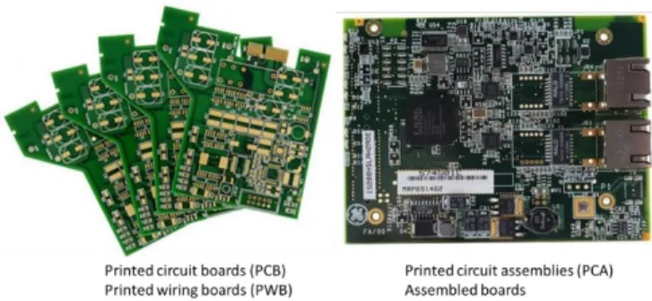
For historical reasons, we refer to the bare circuit board with no components attached as a printed circuit board (PCB) or a printed wiring board (PWB). After the components are attached, it is called a printed circuit assembly (PCA). Examples of PCBs and PCAs are shown in Figure 2.1.
Figure 2.1. The distinction between the terms printed circuit boards and printed circuit assemblies.
In this book, we will cover not just the design of the PCB
interconnects but also the selection of the parts, their assembly, bring up, and test. These elements are part of the successful prototype development process.
2.2 Physical Design of a PCB
A printed circuit board is composed of alternating layers of conductors made of copper foil and dielectrics.
We define the number of layers in a circuit board in terms of how many metal layers are in the board regardless of how they are used.
The simplest circuit board is composed of one conductor layer on a dielectric substrate. More commonly, most simple boards are two layers.
The board layers usually increase by two layers at a time. The next board stack-up is a 4-layer board, then, 6-layer board, and so on.
This is due to the manufacturing process of laminating pairs of layers together to make multilayer boards.
Each dielectric layer is composed of a glass weave yarn impregnated with an epoxy dielectric. This is basically the structure of fiberglass.
The most common dielectric material is called FR-4. This is “fire retardant” style #4.
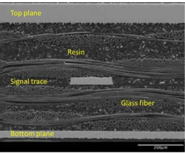
Figure 2.2 shows a cross section of a signal line, copper planes, and the fiberglass dielectric between them. While there are three metal layers shown, this is just part of the board stack-up. On top of these are other metal layers.
2.3 Vias Technologies 41
Figure 2.2. Cross section of a circuit board showing a copper plane on the top and bottom layers, with a signal layer between them. Source is Bogatin Enterprises.
But there is more to a circuit board than just the copper layers and the dielectrics between them.
2.3 Vias Technologies
With signals, power, and ground on multiple layers, electrical connections between layers have to be made with vias. There are three types of commonly used vias in a board, defined by how they are manufactured and what they connect. These three types of vias are illustrated in Figure 2.3.
Figure 2.3. Examples of the three types of vias in a circuit board: (1) blind via, (2) buried via, and (3) through-hole via. Courtesy of Altium.
The most common type of via is a through-hole or plated through- hole (PTH) via. If you do not want metal on a specific layer to connect to the PTH via, add a clearance hole on that layer where the drill passes through the layer. This is done automatically in most routing tools based on net names. The clearance hole in the plane layer is sometimes referred to as an antipad.
To connect two inner layers, such as two ground planes, with a through-hole via, you would make sure there is no trace on the top or bottom layers where the drill passes through the board. The resulting through-hole via would only connect the inner layers.
The residual piece of plated through-hole barrel that sticks up or down from the last connected layer is called a stub. In very high frequency boards, with signals operating above 10 Gbps, the via stubs can be a serious signal integrity problem. However, for all boards operating at 5 Gbps and below, the via stubs are rarely a performance problem and can be ignored.
An example of a 4-layer board constructed with through-hole vias is illustrated in Figure 2.4.
2.3 Vias Technologies 43
Figure 2.4 Example of a 4-layer board with through holes. Courtesy of Altium.
In this example, all the PTH vias drilled in the board go all the way through the board.
All the features and dimensions of the PTH are considered part of the via pad stack design. Unless you have a strong compelling reason otherwise, the features should be:
✓ Drill diameter 13 mils (this makes the finished, plated hole diameter 10.2 mils)
✓ Capture pad diameter around the via on any layer with a connection, 25 mils (6 mil copper annulus around the 13 mil drill diameter)
✓ Clearance annulus on a copper plane with no connection of 6 mils.
Part of the process of plating the via holes requires there be capture pads on the top and bottom layers of the via hole. The capture pad is to provide a larger target for the drill to hit to make up for
registration tolerances. On layers on which there are no connections to be made by the via, there is no need for a capture pad. It is a good habit to remove these non-functional capture pads.
The annulus of the capture cannot be narrower than 6 mils for the lowest cost. This makes the outer diameter of the capture pad 13 mils + 6 mils + 6 mils = 25 mils.
With 6 mils as the narrowest clearance between copper features, the closest spacing between vias is 31 mils. A robust via-to-via pitch to
use is 35 mils. This leaves 10 mils as the spacing between the edges of the via pads.
A buried via typically connects only between two adjacent layers. It is drilled and plated at the time when the 2-layer core is patterned.
This extra drilling and plating step will add cost to the board.
The advantage of the buried via is that it does not block routing channels above and below it. This can be of value in very dense boards and may be worth paying the extra price. Most low-cost fab shops do not offer buried vias. For example, this type of via is NOT an option at JLCpcb.com.
A blind via is drilled from the top of the board to a controlled depth at the same time the through-hole vias are drilled. This makes a small, blind hole, from the top or bottom of the board, stopping on a lower layer.
After drilling, the inside of the hole has to be plated. This is difficult in a blind hole if the aspect ratio is larger than 1 to 1. It requires special chemistry to remove the air bubble in the hole and to get plating fluid to fill the hole and make contact to the exposed layers.
The value of a blind via is that a via can be placed inside a pad to make a low inductance contact to the layer below and it will not block routing channels on other layers.
If you were to add a through-hole via in a pad on which a component is soldered, the quality of the solder joint can be degraded. If there is a plated through-hole via inside a component pad, when the solder paste melts and reflows, the solder may wick down the plated hole by capillary action. This will steal or thieve some of the solder from the pad. This means there is the chance there may not be enough solder left on the pad to make a good solder joint to the component.
This is why a through-hole via should never be placed in a pad if automated assembly will be used.
Blind vias are often used for via-in-pad applications for decoupling capacitors where low loop inductance connections are of high value.
A blind via will not wick solder from a pad and will not cause an
2.4 Thermal and Thermal Relief Vias 45
assembly problem. This is why blind vias are ok to use as via in pad connections.
Via in pad is not an option for many low-cost fab shops since it requires specialized plating chemistry and drilling.
Through-hole vias are the lowest cost and most common type of via. Unless you have a strong compelling reason otherwise, ALWAYS use through-hole vias and never any
other type of via.
2.4 Thermal and Thermal Relief Vias There are really two purposes for a via:
✓ To conduct electrical current from one layer to another
✓ To conduct heat from one layer to another
The main purpose of a via is to provide electrical connectivity. These vias are referred to as just vias. But, when a via is used to conduct heat, it is referred to as a thermal via.
This should not be confused with a thermal relief via. A thermal relief via is a via used for electrical connectivity for which you want to limit the heat conduction.
If a via is connected to a plane, it will normally conduct heat very well to the plane. If this via is also connected to a component that would be soldered, such as with a pin inserted in the via hole, the plane may suck out so much heat as to make soldering very difficult.
For example, if a pin is to be inserted and soldered into a plated through-hole that also connects to a plane, the plane may suck so much heat from the pin as to make soldering the pin almost impossible. We need a way to reduce the thermal conductivity of a via but maintain the electrical conductivity.
How do you engineer a via to be both low electrical resistance but high thermal resistance? This is where a thermal isolation moat with a narrow drawbridge for electrical conduction comes in. An example
of a thermal relief via is shown in Figure 2.5. The narrow tabs provide low electrical resistance, typically less than 0.5 mohms, but high thermal resistance.
Figure 2.5 Example of a thermal relief via.
It is only when the via connects a soldered pin or is inside a solder pad used for the ground connection to a decoupling capacitor, for example, that a thermal relief via needed.
A thermal relief via will take up more room than a normal via. As a good habit, only use a thermal relief via when thermal isolation is also required.
When a via is between a signal trace and a plane and there are no solder pads adjacent to the via, there is no need for a thermal relief via. If the via is connected to a pad through a 6 mil wide trace, 20 mils long, there is no need for a thermal relief via. The trace acts as a thermal relief. If a via is between two signal traces on different layers, there is no need for a via with thermal relief.
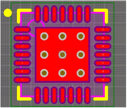
Do not confuse a thermal relief via with a thermal via. A thermal via is used specifically to provide a low thermal resistance between a component and a plane. These vias usually connect the attach pad under a component such as a quad-flat-no lead (QFN) part and a plane underneath. An example of the footprint of a QFN showing the
2.4 Thermal and Thermal Relief Vias 47
thermal vias underneath the component footprint is shown in Figure 2.6.
Figure 2.6 A small footprint QFN part with thermal vias in the center. Be sure to use thermal vias with a diameter at least 13 mils so there is no cost adder.
In many footprints for QFN parts, the thermal vias are by default 8 mil diameter or narrower in the footprint. If you use this footprint on your board, the fab shop may charge a premium price for the entire board just because it has narrow thermal vias. Be sure to change the size of the thermal vias and make them no narrower than 13 mils drill diameter.
Thermal vias act as a heat spreader for small components that may dissipate a lot of power. NEVER use thermal relief structures in a via being used as a thermal via to conduct the heat away from a
component. It will defeat the entire purpose of a thermal via.
2.5 Other Layers
In a 2-layer board, the complete stack-up showing each layer a fab shop needs to return a completed circuit board is shown in Figure 2.7.
Figure 2.7. The complete stack-up of all the layers that must be delivered to the fab shop to return a completed circuit board.
The outline layer defines the shape of the board. It is this structure that is used to separate your specific circuit board in the panel in which it is built from other boards. An endmill will literally drill the board out from the rest of the panel. This is called “routing out” the board, not to be confused with the use of “routing” in regard to drawing traces on the board.
Many fab shops will not commit to fabricate your board without an outline layer. Without the outline layer, the fab shop does not know where your board ends and another customer’s board begins in the large panel in which they are fabricated.
2.6 The Soldermask Layer 49
The drill layer has information about what hole sizes are used for each hole and their precise location, and is used by a precision CNC drilling machine to drill every hole in the board.
The silk screen is sometimes referred to as the overlay layer on both the top and bottom of the board. This is the printed text or numbers that identity each part and any other written reference information.
It can also include images, logos, and pictures.
The soldermask is a layer of dielectric with small openings in it to reveal the underlying metal. Components will be soldered to pads exposed in the open areas of soldermask. The soldermask coating prevents the solder from flowing over the rest of the covered copper traces.
A very good review article that introduces many of the terms used in printed circuit boards can be found here,
http://www.pcb.electrosoft-engineering.com/04-articles-custom- system-design-and-pcb/01-printed-circuit-board-concepts/printed- circuit-board-pcb-concepts.html
Download this short ebook here , https://www.asc- i.com/fundamentals-pcb-tech/download-e-book
2.6 The Soldermask Layer
On top of the copper layer is a soldermask that covers the entire surface of copper so it cannot be coated with solder, except for small windows made in the soldermask. These windows expose the pad on to which will be soldered the components.
The purpose of the soldermask is to keep solder only where it is supposed to be, the component attach pads, and not where it
shouldn’t be, the interconnect traces. If it weren’t for the soldermask, solder would spread across the traces and not enough solder would stay on the pads to make a reliable solder joint for the component.
The soldermask can also sometimes prevent solder bridging between closely spaced pads.