Ata Elahi
Computer Systems
Digital Design, Fundamentals of
Computer Architecture and Assembly
Language
Computer Systems
Computer Systems
Digital Design, Fundamentals of Computer
Architecture and Assembly Language
Ata Elahi
Southern Connecticut State University New Haven, CT, USA
ISBN 978-3-319-66774-4 ISBN 978-3-319-66775-1 (eBook) https://doi.org/10.1007/978-3-319-66775-1
Library of Congress Control Number: 2017952347
©Springer International Publishing AG 2018
This work is subject to copyright. All rights are reserved by the Publisher, whether the whole or part of the material is concerned, specifically the rights of translation, reprinting, reuse of illustrations, recitation, broadcasting, reproduction on microfilms or in any other physical way, and transmission or information storage and retrieval, electronic adaptation, computer software, or by similar or dissimilar methodology now known or hereafter developed.
The use of general descriptive names, registered names, trademarks, service marks, etc. in this publication does not imply, even in the absence of a specific statement, that such names are exempt from the relevant protective laws and regulations and therefore free for general use.
The publisher, the authors and the editors are safe to assume that the advice and information in this book are believed to be true and accurate at the date of publication. Neither the publisher nor the authors or the editors give a warranty, express or implied, with respect to the material contained herein or for any errors or omissions that may have been made. The publisher remains neutral with regard to jurisdictional claims in published maps and institutional affiliations.
Printed on acid-free paper
This Springer imprint is published by Springer Nature
The registered company is Springer International Publishing AG
The registered company address is: Gewerbestrasse 11, 6330 Cham, Switzerland
Sara, Shabnam and Aria
Preface
This textbook is the result of my experiences teaching computer systems at the Computer Science Department at Southern Connecticut State University since 1986. The book is divided into three sections: Digital Design, Introduction to Computer Architecture and Memory, and ARM Architecture and Assembly Lan- guage. The Digital Design section includes a laboratory manual with 12 experi- ments using Logisim software to enforce important concepts. The ARM Architecture and Assembly Language section includes several examples of assem- bly langauge programs using KeilμVision 5 development tools.
Intended Audience
This book is written primarily for a one semester course as an introduction to computer hardware and assembly language for students majoring in Computer Science, Information Systems and Engineering Technology.
Organization
The material of this book is presented in such a way that no special background is required to understand the topics.
Chapter 1–Signals and Number Systems: Analog Signal, Digital Signal, Binary Numbers, Addition and Subtraction of binary numbers, IEEE 754 Floating Point representations, ASCII, Unicode, Serial Transmission, and Parallel Transmission.
Chapter 2–Boolean Logics and Logic Gates: Boolean Logics, Boolean Algebra Theorems, Logic Gates, Integrate Circuit (IC), Boolean Function, Truth Table of a function and using Boolean Theorems to simplify Boolean Functions.
vii
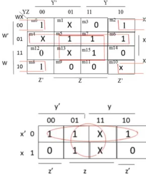
Chapter 3 – Minterms, Maxterms, Karnaugh Map (K-Map) and Universal Gates: Minterms, Maxterms, Karnaugh Map (K-Map) to simplify Boolean Func- tions, Don’t Care Conditions and Universal Gates.
Chapter 4– Combinational Logic: Analysis of Combination Logic, Design of Combinational Logic, Decoder, Encoder, Multiplexer, Half Adder, Full Adder, Binary Adder, Binary Subtractor, Designing Arithmetic Logic Unit (ALU) and BCD to Seven Segment Decoder.
Chapter 5–Synchronous Sequential Logic: Sequential Logic such as S-R Latch, D-Flip Flop, J-K Flip Flop, T-Flip Flop, Register, Shift Register, Analysis of Sequential Logic, State Diagram, State Table, Flip Flop Excitation Table and Designing Counter.
Chapter 6– Introduction to Computer Architecture: Components of a Micro- computer, CPU Technology, CPU Architecture, Instruction Execution, Pipelining, PCI, PCI Express, USB, and HDMI.
Chapter 7–Memory: Memory including RAM, SRAM, DISK, SSD, Memory Hierarchy, Cache Memory, Cache Memory Mapping Methods, Virtual Memory, Page Table and the memory organization of a computer.
Chapter 8–ARM Architecture and Instructions Part I: ARM Processor Archi- tecture, and ARM Instruction Set such as Data Processing, Shift, Rotate, Uncondi- tional Instructions and Conditional Instructions, Stack Operation, Branch, Multiply Instructions and several examples of converting HLL to Assembly language.
Chapter 9 – ARM Instructions Part II: This chapter is the continuation of Chapter 8 which covers Load and Store Instructions, Pseudo Instructions, ARM Addressing Mode and data representation in memory.
Chapter 10–ARM Assembly Language Programming Using Keil Development Tools: Covers how to use Keil development software for writing assembly language using ARM Instructions, Compiling Assembly Language and Debugging.
Instruction Resources: The instruction resources contains
• Laboratory experiments using Logisim.
• Solutions to the problems of each chapter.
New Haven, CT, USA Ata Elahi
Acknowledgments
I would like to express my special thanks to Professor Lancor Chairman of Computer Science Department at Southern Connecticut State University for her support as well as Professor Herv Podnar for his guidance.
I wish to acknowledge and thank Ms. Mary E. James, Senior Editor in Applied Sciences and her assistant, Ms. Zoe Kennedy, for their support.
My special thanks to Marc Gajdosik, Nickolas Santini, Nicholas Bittar, Eric Basini, Omar Abid and Alireza Ghods for their help in developing the manuscript.
Finally, I would like to thank the students of CSC 207 Computer Systems of Spring 2017.
ix
1 Signals and Number Systems. . . 1
1.1 Introduction . . . 1
1.2 Analog Signals . . . 2
1.2.1 Characteristics of an Analog Signal . . . 3
1.3 Digital Signals . . . 5
1.4 Number System . . . 5
1.4.1 Converting from Binary to Decimal . . . 6
1.4.2 Converting from Decimal Integer to Binary . . . 7
1.4.3 Converting Decimal Fraction to Binary . . . 8
1.4.4 Converting from Hex to Binary . . . 9
1.4.5 Binary Addition . . . 10
1.5 Complement and Two’s Complement . . . 11
1.5.1 Subtraction of Unsigned Number Using Two’s Complement . . . 11
1.6 Unsigned, Signed Magnitude, and Signed Two’s Complement Binary Number . . . 12
1.7 Binary Addition Using Signed Two’s Complement . . . 13
1.8 Floating Point Representation . . . 14
1.8.1 Single Precision Representation . . . 15
1.9 Binary-Coded Decimal (BCD) . . . 16
1.10 Coding Schemes . . . 17
1.10.1 ASCII Code . . . 17
1.10.2 Universal Code or Unicode . . . 17
1.11 Parity Bit . . . 21
1.12 Clock . . . 21
1.13 Transmission Modes . . . 22
1.13.1 Asynchronous Transmission . . . 22
1.13.2 Synchronous Transmission . . . 23
xi
1.14 Transmission Methods . . . 23
1.14.1 Serial Transmission . . . 24
1.14.2 Parallel Transmission . . . 24
1.15 Summary . . . 24
2 Boolean Logics and Logic Gates. . . 29
2.1 Introduction . . . 29
2.2 Boolean Logics and Logic Gates . . . 30
2.3 Integrated Circuit (IC) Classifications . . . 33
2.4 Boolean Algebra Theorems . . . 36
2.5 Boolean Function . . . 39
2.6 Summary . . . 40
3 Minterms, Maxterms, Karnaugh Map (K-Map), and Universal Gates. . . 47
3.1 Introduction . . . 47
3.2 Minterms . . . 48
3.3 Maxterms . . . 51
3.4 Karnaugh Map (K-Map) . . . 52
3.4.1 Three-Variable Map . . . 53
3.4.2 Four-Variable K-Map . . . 57
3.5 Sum of Products (SOP) and Product of Sums (POS) . . . 58
3.6 Don’t CareConditions . . . 60
3.7 Universal Gates . . . 61
3.7.1 Using NAND Gates . . . 62
3.7.2 Using NOR Gates . . . 63
3.7.3 Implementation of Logic Functions Using NAND Gates or NOR Gates Only . . . 64
3.7.4 Using NAND Gates . . . 64
3.7.5 Using NOR Gates . . . 65
3.8 Summary . . . 66
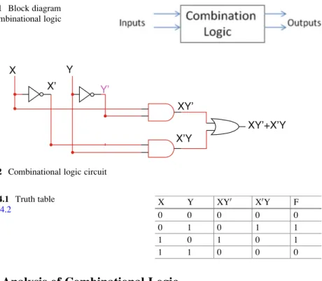
4 Combinational Logic. . . 71
4.1 Introduction . . . 71
4.2 Analysis of Combinational Logic . . . 72
4.3 Design of Combinational Logic . . . 72
4.4 Decoder . . . 75
4.4.1 Implementing a Function Using a Decoder . . . 76
4.5 Encoder . . . 76
4.6 Multiplexer (MUX) . . . 77
4.6.1 Designing Large Multiplexer Using Smaller Multiplexers . . . 81
4.6.2 Implementing Functions Using Multiplexer . . . 83
4.7 Half Adder, Full Adder, Binary Adder, and Subtractor . . . 84
4.7.1 4-Bit Binary Adder . . . 87
4.7.2 Subtractor . . . 88
xii Contents
4.8 ALU (Arithmetic Logic Unit) . . . 88
4.9 Seven-Segment Display . . . 89
4.10 Summary . . . 92
5 Synchronous Sequential Logic. . . 97
5.1 Introduction . . . 97
5.2 S-R Latch . . . 98
5.3 D Flip-Flop . . . 99
5.4 J-K Flip-Flop . . . 100
5.5 T Flip-Flop . . . 101
5.6 Register . . . 101
5.7 Frequency Divider Using J-K Flip-Flop . . . 102
5.8 Analysis of Sequential Logic . . . 104
5.9 State Diagram . . . 106
5.10 Flip-Flop Excitation Table . . . 107
5.11 Counter . . . 108
5.12 Summary . . . 110
6 Introduction to Computer Architecture. . . 115
6.1 Introduction . . . 115
6.2 Components of a Microcomputer . . . 115
6.2.1 Central Processing Unit (CPU) . . . 116
6.2.2 CPU Buses . . . 116
6.2.3 32-Bit Versus 64-Bit CPU . . . 118
6.3 CPU Technology . . . 118
6.4 CPU Architecture . . . 120
6.5 Intel Microprocessor Family . . . 120
6.6 Multicore Processors . . . 122
6.7 CPU Instruction Execution . . . 123
6.8 Disk Controller . . . 125
6.9 Microcomputer Bus . . . 126
6.9.1 ISA Bus . . . 127
6.9.2 Microchannel Architecture Bus . . . 127
6.9.3 EISA Bus . . . 127
6.9.4 VESA Bus . . . 127
6.9.5 PCI Bus . . . 127
6.9.6 Universal Serial BUS (USB) . . . 128
6.9.7 USB Architecture . . . 129
6.9.8 PCI Express Bus . . . 131
6.9.9 PCI Express Architecture . . . 131
6.9.10 PCI Express Protocol Architecture . . . 132
6.10 FireWire . . . 132
6.10.1 HDMI (High-DefinitionMultimediaInterface) . . . 133
6.11 Summary . . . 133
7 Memory. . . 137
7.1 Introduction . . . 137
7.2 Semiconductor Memory . . . 137
7.3 Hard Disk . . . 142
7.4 Solid-State Drive (SSD) . . . 144
7.5 Memory Hierarchy . . . 144
7.5.1 Virtual Memory . . . 153
7.5.2 Memory Organization of a Computer . . . 155
8 Assembly Language and ARM Instructions Part I. . . 161
8.1 Introduction . . . 161
8.2 Instruction Set Architecture (ISA) . . . 162
8.2.1 Classification of Instruction Based on Number of Operands . . . 162
8.3 ARM Processor Architecture . . . 163
8.4 ARM Registers . . . 165
8.5 ARM Instructions . . . 166
8.5.1 Data Processing Instructions . . . 167
8.5.2 Compare and Test Instructions . . . 169
8.5.3 Register Swap Instructions (MOV and MVN) . . . 170
8.5.4 Shift and Rotate Instructions . . . 171
8.5.5 ARM Unconditional Instructions and Conditional Instructions . . . 173
8.6 ARM Data Processing Instruction Format . . . 174
8.7 Stack Operation and Instructions . . . 177
8.8 Branch (B) and Branch with Link Instruction (BL) . . . 178
8.8.1 B and BL Instruction Format . . . 179
8.9 Multiply (MUL) and Multiply-Accumulate (MLA) Instructions . . . 180
8.9.1 Multiply Instruction Format . . . 180
8.10 Summary . . . 181
8.11 Problems and Questions . . . 181
9 ARM Instructions Part II. . . 185
9.1 Introduction . . . 185
9.2 ARM Data Transfer Instructions . . . 185
9.2.1 ARM Pseudo Instructions . . . 186
9.2.2 Store Instructions (STR) . . . 187
9.3 ARM Addressing Mode . . . 187
9.3.1 Immediate Addressing . . . 188
9.3.2 Pre-indexed . . . 188
9.3.3 Pre-indexed with Write Back . . . 189
9.3.4 Post-index Addressing . . . 190
9.4 Swap Memory and Register (SWAP) . . . 191
xiv Contents
9.5 Bits Field Instructions . . . 191
9.5.1 BFC (Bit Field Clear Instruction) . . . 191
9.5.2 BFI (Bit Insertion Instruction) . . . 192
9.6 Data Representation and Memory . . . 192
9.7 Summary . . . 194
10 ARM Assembly Language Programming Using Keil Development Tools. . . 197
10.1 Introduction . . . 197
10.2 Keil Development Tools for ARM Assembly . . . 198
10.2.1 Assembling a Program . . . 201
10.2.2 Running the Debugger/Simulator . . . 204
10.2.3 Program Template . . . 208
10.3 Programming Rules . . . 208
10.4 Data Representation and Memory . . . 209
10.5 Directives . . . 209
10.5.1 Data Directive . . . 210
10.6 Memory inμVision v5 . . . 211
10.7 Summary . . . 212
Appendix: Digital Design Laboratory Experiments Using LOGISIM. . . 217
References. . . 255
Index. . . 257
Chapter 1
Signals and Number Systems
Objectives: After completing this chapter, you should be able to:
• Explain the basic components of a computer.
• Distinguish between analog and digital signal.
• Learn the characteristics of signal.
• Convert decimal numbers to binary and vice versa.
• Learn addition and subtraction of binary numbers.
• Represent floating numbers in binary.
• Convert from binary to hexadecimal and vice versa.
• Distinguish between serial and parallel transmission.
1.1 Introduction
Numerical values have become an integral part of our daily lives. Numerical values can be represented by analog or digital; examples include an analog watch, digital watch, or thermometer. The following are advantages of digital representation of numerical values compared to analog representation:
1. Digital representation is more accurate.
2. Digital information are easier to store 3. Digital systems are easier to design.
4. Noise has less effect.
5. Digital systems can easily be fabricated in an integrated circuit.
A digital signal is a discrete signal (step by step), and an analog signal is a continuous signal. Digital systems are widely used and its applications can be seen in computers, calculators, and cell phones. In a digital system, information is transferred between components of the digital system in the form of digital signals.
©Springer International Publishing AG 2018
A. Elahi,Computer Systems,https://doi.org/10.1007/978-3-319-66775-1_1
1
A computer consists of two components: hardware and software. Hardware refers to the physical components of a computer such as the keyboard, CPU, and memory. Software refers to programs run by CPU including operating systems and application programs. Computers can come in several different forms such as a desktop, laptop, tablet, server, and iPhone. Regardless of the form, all computers consist of the same basic structures. Figure1.1shows the basic components of a computer.
Input Device The input device is used for entering information into memory.
Examples of input devices include the keyboard, mouse, touch pad screen, light pen, barcode reader, and scanner. The input device converts information into bits, and the bits are stored in memory.
Output Device A computer’s memory transfers information to theoutput devicein the form of bits. The output device converts bits to characters, images, and voices which can be interpreted by humans.
Memory Memory is used to store information and programs. Memory comes in the form of solid-state electronics such as RAM, ROM, flash drive, or hard disk.
The Central Processing Unit (CPU) The CPU is used to perform computations on information.
1.2 Analog Signals
An analog signal is a signal whose amplitude is a function of time and changes gradually as time changes. Analog signals can be classified as nonperiodic and periodic signals.
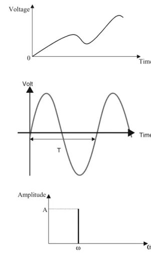
Nonperiodic Signal In a nonperiodic signal, there is no repeated pattern in the signal as shown in Fig.1.2.
Periodic Signal A signal that repeats a pattern within a measurable time period is called a periodic signal, and completion of a full pattern is called a cycle. The simplest periodic signal is a sine wave, which is shown in Fig.1.3. In the time domain, the sine wave amplitudea(t) can be represented mathematically asa(t)¼ A Sin(ωtþθ) where A is the maximum amplitude,ωis the angular frequency, and θis the phase angle.
Fig. 1.1 Basic components of a computer
A periodic signal can also be represented in the frequency domain where the horizontal axis is the frequency and the vertical axis is the amplitude of the signal.
Figure1.4shows the frequency domain representation of a sine wave signal.
An electrical signal, usually representing voice, temperature, or a musical sound, is made of multiple wave forms. These signals have one fundamental frequency and multiple frequencies that are called harmonics.
1.2.1 Characteristics of an Analog Signal
The characteristics of a periodic analog signal are frequency, amplitude, and phase.
Frequency Frequency (F) is the number of cycles in 1 s,F¼1T, represented in Hz (Hertz). If each cycle of an analog signal is repeated every 1 s, the frequency of the signal is 1 Hz. If each cycle of an analog signal is repeated 1000 times every second (once every millisecond), the frequency is
Time Voltage
0 Fig. 1.2 Representation of
a nonperiodic analog signal
T Volt
Time Fig. 1.3 Time domain
representation of a sine wave
Amplitude
ω
ω A
Fig. 1.4 Frequency representation of a sine wave
1.2 Analog Signals 3
f ¼1 T ¼ 1
103 ¼1000 Hz¼1 kHz
Table1.1shows different values for frequency and their corresponding periods.
Amplitude The amplitude of an analog signal is a function of time as shown in Fig. 1.5 and may be represented in volts (unit of voltage). In other words, the amplitude is its voltage value at any given time. At the timet1, the amplitude of the signal isV1.
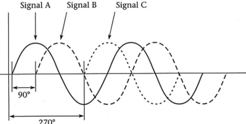
Phase Two signals with the same frequency can differ in phase. This means that one of the signals starts at a different time from the other one. This difference can be represented in degrees (0 to 360) or by radians. A phase angle of 0 indicates that the sine wave starts at time 0, and a phase angle of 90indicates that the signal starts at 90as shown in Fig.1.6.
Example 1.1 Find the equation for a sine wave signal with a frequency of 10 Hz, maximum amplitude of 20 volts, and phase angle of 0:
Table 1.1 Typical units of frequency and period
Units of frequency Numerical value Units of period Numerical value
Hertz (Hz) 1 Hz Second (s) 1 s
Kilohertz (kHz) 103Hz Millisecond (ms) 103s
Megahertz (MHz) 106Hz Microsecond (μs) 106s
Gigahertz (GHz) 109Hz Nanosecond (ns) 109s
Terahertz (THz) 1012Hz Picosecond (ps) 1012s
T/2 3T/4 T
t
-A a(t)
t1= T/4 V1=+A
Fig. 1.5 A sine wave signal over one cycle
ω¼2πf ¼23:141610¼62:83 rad sec a tð Þ ¼20 sin 62ð :83tÞ
1.3 Digital Signals
Modern computers communicate by using digital signals. Digital signals are represented by two voltages: one voltage represents the number 0 in binary, and the other voltage represents the number 1 in binary. An example of a digital signal is shown in Fig.1.7, where 0 volts represents 0 in binary andþ5 volts represents 1. 0 or 1 is called a bit and 8 bits is called a byte.
1.4 Number System
Numbers can be represented in different bases. A base of ten is called a decimal. In the example, below consider 356 in decimal:
Fig. 1.6 Three sine waves with different phases
+5
1 0 0 1 1 1 0 1
0 time
Fig. 1.7 Digital signal
1.4 Number System 5
356¼6þ50þ300¼6∗100þ5∗101þ3∗102 In general, a number can be represented in the form:
a5a4a3a2a1a0:a1a2a3
ð Þr,
where r is the base of the number and aimust be less than r.
(10011)2is a valid number but (211.01)2is not.
Equation1.1can be used to convert a number in a given base to decimal:
ða|fflfflfflfflfflfflfflfflffl{zfflfflfflfflfflfflfflfflffl}5a4a3a2a1a0 Integer
:a|fflfflfflfflfflffl{zfflfflfflfflfflffl}1a2a3 Fraction
Þr¼a0r0þa1r1þa2r2þa3r3þ. . .
þa1r1þa2r2þ a2r3. . .
ð1:1Þ
Example 1.2 Convert (27.35)8to the base of 10.
27:35
ð Þ8¼7∗80þ2∗81þ3∗81þ5∗82¼7þ16þ:375þ:078125
¼ð23:45Þ10
Example 1.3 Convert 1101111 to decimal.
1101111
ð Þ2¼1∗20þ1∗21þ1∗22þ1∗23þ0∗24þ1∗25þ1∗26
¼1þ2þ4þ8þ32þ64¼ð111Þ10
1.4.1 Converting from Binary to Decimal
Equation1.2represents the general form of a binary number:
a5a4a3a2a1a0:a1a2a3
ð Þ2 ð1:2Þ
where aiis a binary digit or bit (either 0 or 1).
Equation1.2can be converted to decimal number by using Eq.1.1:
ða|fflfflfflfflfflfflfflfflffl{zfflfflfflfflfflfflfflfflffl}5a4a3a2a1a0 Integer
:a|fflfflfflfflfflffl{zfflfflfflfflfflffl}1a2a3 Fraction
Þ2 ¼a020þa121þa222þa323þ. . .
þa121þa222þ. . .
ð1:3Þ
a5a4a3a2a1a0:a1a2a3
ð Þ2¼a0þ2 a1þ4 a2þ8 a3þ16 a4þ32 a5þ64 a6
þ1
2∗a1þ1
4∗a2þ1 8∗a3 Example 1.4 Convert (110111.101)2to decimal.
110111:101
ð Þ2¼1∗20þ1∗21þ1∗22þ0∗23þ1∗24þ1∗2∗5þ1∗21 þ0∗22þ1∗23
¼55:625 Or
25 24 23 22 21 20 21 22 23
1 1 0 1 1 1 . 1 0 1
32þ16þ0þ4þ2þ1þ1=2þ0þ1=8
If a binary value is made of n bits of ones, then its decimal value is 2n1.
Example 1.5
11¼221¼3 111¼231¼7 1111¼241¼15 11111¼251¼31 111111¼261¼63
Binary, or base of 2 numbers, is represented by 0s and 1s. A binary digit, 0 or 1, is called a bit, 8 bits is called a byte, 16 bits is called a half word, and 4 bytes is called a word.
1.4.2 Converting from Decimal Integer to Binary
To convert an integer number from decimal to binary, divide the decimal number by the new base (2 for binary), which will result in a quotient and a remainder (either 0 or 1). The first remainder will be the least significant bit of the binary number. Continually divide the quotient by the new base, while taking the remain- ders as each subsequent bit in the binary number, until the quotient becomes 0.
1.4 Number System 7
Example 1.6 Convert 34 in decimal to binary.
Quotient Remainder
34/2¼ 17 0¼a0
17/2¼ 8 1¼a1
8/2 4 0¼a2
4/2 2 0¼a3
2/2 1 0¼a4
1/2 0 1¼a5
Therefore 34¼(100010)2
If a binary number is made of all ones, then by using the equation 2n1, it can be converted to decimal.
Examples
Binary number 2n1 Decimal number
11 22–1 3
111 23–1 7
1111 24–1 15
11111 25–1 32
A binary number is represented by a5a4a3a2a1a0where a0is 20, a1is 21, and a5is 25. Table1.2shows 2n.
1.4.3 Converting Decimal Fraction to Binary
A decimal number representation of (0.XY)10can be converted into base of 2 and represented by (0.a1, a2, a3, etc.)2.
The fraction number is multiplied by 2, the result of integer part is a1 and fraction part multiply by 2, and then separate integer part from fraction, the integer part represents a2; this process continues until the fraction becomes 0.
(0.35)10¼( )2
0.35*2 ¼ 0.7 ¼ 0 þ 0.7 a1¼0
0.7*2 ¼ 1.4 ¼ 1 þ 0.4 a2¼1
0.4*2 ¼ 0.8 ¼ 0 þ 0.8 a3¼0
0.8*2 ¼ 1.6 ¼ 1 þ 0.6 a4¼1
0.6*2 ¼ 1.2 ¼ 1 þ 0.2 a5¼1
Sometimes, the fraction does not reach 0 and the number of bits use for the fraction depends on the accuracy that the user defines, therefore the 0.35 ¼ 0.010011 in binary
The hexadecimal number system has a base of 16 and therefore has 16 symbols (0 through 9, and A through F). Table1.3shows the decimal numbers, their binary values from 0 to 15, and their hexadecimal equivalents.
1.4.4 Converting from Hex to Binary
Table1.3can also be used to convert a number from hexadecimal to binary and from binary to hexadecimal.
Example 1.7 Convert the binary number 001010011010 to hexadecimal. Each 4 bits are grouped from right to left. By using Table 2.2, each 4-bit group can be converted to its hexadecimal equivalent.
Table 1.2 2nwith different values of n
2n Decimal value 2n Decimal value 2n Decimal value
20 1 28 256 216 65,536¼64 K
21 2 29 512 217 131,072¼128 K
22 4 210 1024¼1 K 218 262,144¼256 K
23 8 211 2048¼2 K 219 524,288¼512 K
24 16 212 4096¼4 K 220 1,048,576¼1 M
25 32 213 8192¼8 K 221 2 M
26 64 214 16,384¼16 K 222 4 M
27 128 215 32,768¼32 K 223 8 M
Table 1.3 Decimal numbers with binary and hexadecimal equivalents
Decimal Binary (base of 2) Hexadecimal (base of 16) or HEX
0 0000 0
1 0001 1
2 0010 2
3 0011 3
4 0100 4
5 0101 5
6 0110 6
7 0111 7
8 1000 8
9 1001 9
10 1010 A
11 1011 B
12 1100 C
13 1101 D
14 1110 E
15 1111 F
1.4 Number System 9
0010 1001 1010
2 9 A
Example 1.8 Convert (3D5)16to binary. By using Table 2.2, the result in binary is:
3 D 5
0011 1101 0101
The resulting binary number is 001111010101.
Example 1.9 Convert 6DB from hexadecimal to binary. By using Table1.3, the result in binary is:
6 D B
0110 1101 1011
The resulting binary number is 011011011011.
Example 1.10 Convert (110111.101)2to decimal.
110111:101
ð Þ2¼1∗20þ1∗21þ1∗22þ0∗23þ1∗24þ1∗2∗5þ1∗21 þ0∗22þ1∗23
¼55:625
1.4.5 Binary Addition
1þ0¼1, 1þ1¼10, Carry bits 11 1
10101 þ 01101 100010
In a binary number, the first bit from the left of number is called the most significant bit (MSb), and the first bit from the right of number is called least significant bit (LSb).
MSb!1 0 0 1 0 LSb
1.5 Complement and Two ’ s Complement
The complement of 1 is 0 and the complement of 0 is 1.
The complement of a binary number is calculated by complementing each bit of the number.
Example 1.11 The complement of 101101 is 010010.
Two’sComplement ofanumber¼Complement ofanumberþ1
Example 1.12 The two’s complement of 101011 is 010100 complementð Þ þ1¼010101 Example 1.13 Find the two’s complement of 10000:
01111 complementð Þ þ1¼10000
1.5.1 Subtraction of Unsigned Number Using Two ’ s Complement
The following procedure is used to subtract B¼b5b4b3b2b1b0from A¼a5a4a3 a2a1a0:
1. Add two’s complement of B to the A.
2. Check to see if the result produces a carry:
(a) If the result produces a carry, discard the carry and the result is positive.
(b) If the result does not produce a carry, take two’s complement of the result, and the result is negative.
Example 1.14 Subtract B¼101010 from A¼110101.
01010 1¼Complement of B Two’s complement of B¼010101þ1¼010110 Add two’s complement of B to A.
1.5 Complement and Two’s Complement 11
110101 + 010110 ---
10 01011
Carry, discard the carry and the result isþ001011.
Example 1.15 Subtract B¼110101 from A¼101010.
Two’s complement of B is 001010þ1¼001011.
Add two’s complement of B to A.
001011 þ101010 110101
As we can see, adding two 6-bit number results in a 6-bit answer. There is no carry; we just take the two’s complement of the result.
Two’s Complement of 110101¼001010þ1¼ 001011
1.6 Unsigned, Signed Magnitude, and Signed Two ’ s Complement Binary Number
A binary number can be represented in form unsigned number or signed number or signed two’s complement,þsign represented by 0 and – sign represented by 1.
Unsigned Number In an unsigned number, all bits of a number are used to represent the number, but in a signed number, the most significant bit of the number represents the sign. A 1 in the most significant position of number represents a negative sign, and 0 in the most significant position of number represents a positive sign.
The 1101 unsigned value is 13.
Signed Magnitude Number In a signed number, the most significant bit repre- sents the sign, where 1101¼ 5 or 0101¼ þ5
In unsigned number, 1101¼13.
Signed Two’s Complement A signed two’s complement applies to a negative number. If the sign of the number is one, then the number is represented by signed two’s complement.
Example 1.16 Representing (5)10with 4 bits in signed two’s complement.
(5)10in signed number is 1101, then the two’s complement of 101 is 011, and by adding sign bit results in 1011 which represents5 in signed two’s complement.
Example 1.17 Represent (23)10with an 8-bit signed two’s complement.
(23)10¼(1 0 1 1 1)2in unsigned base-2
(100 10111)2– Extended to signed 8 bits (notice theMSbis1) the two’s complement of (0010111)2is (1101001)2
(11101001)2is (23)10insignedtwo’s complement.
1.7 Binary Addition Using Signed Two ’ s Complement
The following examples show the results of the addition of two signed numbers:
(a) (þ3)þ(þ4)
Represent both numbers in binary, and the most significant bit represents the sign, and the result is positive.
0011þ0100¼0111¼ þ7 (b) (þ3)10þ(4)10
(4)10in signed two’s complement is 1100, then
0011þ1100¼1111; result does not generate carry of then take two’s comple- ment of result which is1
3
ð Þ þ þð Þ ¼5 1101þ0101¼1 0010 discard carry and result isð þ2Þ
(c) (7)10þ(5)10
By representing both numbers in 4-bit signed two’s complement, 7
ð Þ10 ¼1001 5
ð Þ10 ¼1011 1001þ1011¼10100
"
Sign bit
The addition of two negative numbers results positive, and it is called overflow:
1.7 Binary Addition Using Signed Two’s Complement 13
þ7
ð Þ þ þð Þ ¼6 ð0111Þ þð0110Þ ¼1101
The addition of two positive numbers results negative, and it is called overflow:
Example 1.18 A. Following addition using 8-bit signed two’s complement (38)10þ(44)10
38
ð Þ10in signed two’s complement ¼11011010 þ44
ð Þ10 þ 00101100
100000110 discard the carry and result is 00000110¼6
B. Add38 to44 using 8 bit signed two’s complement 38 ¼ 11011010
44 ¼ 11010100 --- 10101110¼ 82 C. Addþ100 toþ44
100 ¼ 01100100 44 ¼ 00101100 ---
10010000 the sign of result is negative then results produce overflow
¯¯¯¯¯¯¯¯¯¯¯¯¯¯¯¯¯¯¯¯¯¯¯¯¯¯¯¯¯¯¯¯¯¯¯¯¯¯¯¯¯¯¯¯¯¯¯¯¯¯¯¯¯¯¯¯¯¯¯¯¯¯¯¯¯¯¯¯¯¯¯¯¯¯¯¯¯¯¯¯¯¯¯¯¯¯¯¯¯¯¯¯¯¯¯¯¯¯¯¯¯¯¯¯¯¯¯¯¯¯¯¯¯¯¯¯¯¯¯¯¯¯¯¯¯¯¯¯¯¯¯¯¯¯¯¯¯¯¯¯¯¯
Addition Overflow The following cases result overflow for adding two signed numbers if:
(a) Both numbers are negative, and results of addition become positive:
A
ð Þ þ ð BÞ ¼ þC
(b) Both numbers are positive, and results of addition become negative:
þA
ð Þ þ þð BÞ ¼ C
1.8 Floating Point Representation
The central processing unit (CPU) typically consists of an arithmetic logic unit (ALU), floating point unit (FLU/FPU), registers, control unit, and the cache memory.
Thearithmetic logic unit performs integer arithmetic operations such as addi- tion, subtraction, and logic operations such as AND, OR, XOR, etc.Integersare whole numbers without fractional components. 1, 2, and 3 are integers, while 0.1, 2.2, and 3.0001 all have fractional components are called floating point numbers.
Thefloating point unitperforms floating point operations. Floating point num- bers have a sign, a mantissa, and an exponent. The Institute of Electrical and Electronics Engineers (IEEE) developed a standard to represent floating point numbers, referred to as IEEE 754. This standard defines a format for both single (32-bit) and double (64-bit) precision floating point numbers. Decimal floating points are represented by M10E, where M is the signed mantissa and E is the exponent.
1.8.1 Single Precision Representation
Floating point numbers in single precision represented by 32 bits as shown in Fig.1.8
Biased Exponent The biased exponent is the exponent þ 127 (01111111)2; therefore, the exponent is represented by a positive number.
Normalized Mantissa The mantissa is represented by 1. M, where M is called normalized mantissa; if M¼00101, then mantissa is 1.00101.
Example 1.19 Find normalized mantissa and biased exponent of (111.0000111)2. 111.0000111 can be written in the form of 1.110000111 * 210
Where
M¼110000111
Biased exponent¼10þ01111111¼10000001 The representation of 111.0000111 in single precision is
1bit 8 bits 23 bits
0 10000001 11000011100000000000000
Example 1.20 Convert the following single precision floating point to decimal number.
101111101 11001000000000000000000 S¼1 means mantissa is negative.
Biased exponent¼01111101.
Exponent¼01111101–01111111¼ 00000010.
Normalized mantissa¼11001000000000000000000.
Mantissa¼1. 11001000000000000000000.
Decimal number¼1.11001000000000000000000 *210¼0.01110011.
Double Precision. In order to increase the accuracy of a floating point number, IEEE 745 offers double precision represented by 64 bits as shown in Fig.1.9.
Biased exponent¼exponentþ1023
1.8 Floating Point Representation 15
Example 1.21 Represent 5.75 in IEEE 745 single precision.
15. 625¼(1111.101)2
1111.101¼ 1.11101101 * 211 S¼1
Normalized mantissa¼0.11101101.
Biased exponent¼11þ01111111¼10000010.
IEEE745 single precision is
1 10000010 1110110100000000000000.
1.9 Binary-Coded Decimal (BCD)
In daily life, we use decimal numbers where the largest digit is 9, which is represented by 1001 in binary. Table 1.4 shows decimal numbers and their corresponding BCD code.
Fig. 1.8 IEEE 745 floating point single precision (S¼represent sign of mantissa. S¼0 means mantissa is positive, and S¼1 means mantissa is negative)
Fig. 1.9 IEEE 745 double precision floating point format
Table 1.4 Binary-coded decimal (BCD)
Decimal BCD
0 0000
1 0001
2 0010
3 0011
4 0100
5 0101
6 0110
7 0111
8 1000
9 1001
Example 1.21 Converting 345 to BCD Using the table: 0011 0100 0101
Example 1.22 Convert (10100010010)BCDto decimal, separate each 4 bits from right to left, and substitute the corresponding decimal number with BCD the results in 512.
1.10 Coding Schemes 1.10.1 ASCII Code
Each character in ASCII code has a representation using 8 bits, where the most significant bit is used for a parity bit. Table 1.5 shows the ASCII code and its hexadecimal equivalent.
Characters from hexadecimal 00 to 1F and 7F are control characters which are nonprintable characters, such as NUL, SOH, STX, ETX, ESC, and DLE (data link escape).
Example 1.23 Convert the word “network” to binary and show the result in hexadecimal. By using Table1.4, each character is represented by 7 bits and results in:
1001110 1100101 1110100 1110111 1101111 1110010 1101011
N e t w o r k
Or in hexadecimal
4E 65 74 77 6F 72 6B
1.10.2 Universal Code or Unicode
Unicode is a new 16-bit character-encoding standard for representing characters and numbers in most languages such as Greek, Arabic, Chinese, and Japanese. The ASCII code uses 8 bits to represent each character in Latin, and it can represent 256 characters. The ASCII code does not support mathematical symbols and scientific symbols. SinceUnicodeuses 16 bits, it can represent 65,536 characters or symbols. A character in Unicode is represented by 16-bit binary, equivalent to 4 digits in hexadecimal. For example, the character B in Unicode is U0042H (U represents Unicode). The ASCII code is represented between (00)16 and (FF)16. For converting ASCII code to Unicode, two zeros are added to the left side of ASCII code; therefore, the Unicode to represent ASCII characters is
1.10 Coding Schemes 17
Table1.5AmericanStandardCodeforInformationInterchange(ASCII) BinaryHexCharBinaryHexCharBinaryHexCharBinaryHexChar 000000000NUL010000020SP100000040@110000060, 000000101SOH010000121!100000141A110000161a 000001002STX010001022”100001042B110001062b 000001103ETX010001123#100001143C110001163c 000010004EOT010010024$100010044D110010064d 000010105ENQ010010125%100010145E110010165e 000011006ACK010011026&100011046F110011066f 000011107BEL010011127’100011147G110011167g 000100008BS010100028(10010008H110100068h 000100109HT010100129)100100149I110100169i 00010100ALF01010102A*10010104AJ11010106Aj 00010110BVT01010112Bþ10010114BK11010116Bk 00011000CFF01011002C,10011004CL11011006Cl 00011010DCR01011012D-10011014DM11011016Dm 00011100ESO01011102E.10011104EN11011106En 00011110FSI01011112F/10011114FO11011116Fo 001000010DLE0110000300101000050P111000070P 001000111DC10110001311101000151Q111000171q 001001012DC20110010322101001052R111001072r 001001113DC30110011333101001153S111001173s 001010014DC40110100344101010054T111010074t 001010115NACK0110101355101010155U111010175u 001011016SYN0110110366101011056V111011076v 001011117ETB0110111377101011157W111011177w 001100018CAN0111000388101100058X111100078x 001100119EM0111001399101100159Y111100179y
00110101ASUB01110103A:10110105AZ11110107Az 00110111BESC01110113B;10110115B[11110117B[ 00111001CFS01111003C<10111005C\11111007C\ 00111011DGS01111013D¼10111015D]11111017D} 00111101ERS01111103E<10111105E^11111107E~ 00111111FUS01111113F?10111115F-11111117FDEL
1.10 Coding Schemes 19
between (0000)16and (00FF)16. Table1.6shows some of the Unicode for Latin and Greek characters. Unicode is divided into blocks of code, with each block assigned to a specific language. Table1.7shows each block of Unicode for some different languages (Fig.1.10).
Table 1.6 Unicode values for some Latin and Greek characters
Latin Greek
Character Code (hex) Character Code (hex)
A U0041 φ U03C6
B U0042 α U03B1
C U0043 γ U03B3
0 U0030 μ U03 BC
8 U0038 β U03B2
Table 1.7 Unicode block
allocations Start code (hex) End code (hex) Block name
U0000 U007F Basic Latin
U0080 U00FF Latin supplement
U0370 U03FF Greek
U0530 U058F Armenian
U0590 U05FF Hebrew
U0600 U06FF Arabic
U01A0 U10FF Georgian
Fig. 1.10 Example of Unicode
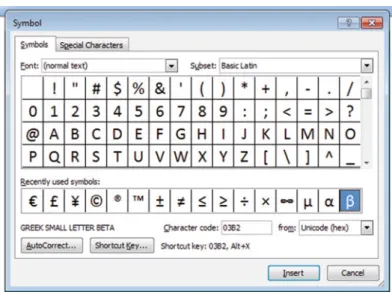
Example of Unicode: open Microsoft Word and click on insert then symbol will result Fig. 1.10. Click on any character to display the Unicode value of the character, for example, Unicode forβis 03B2 in hex
1.11 Parity Bit
A parity bit is used for error detection of information, since a bit or bits may be changed during the transmission of information from source to destination, a parity bit is an extra bit appended to the information. It represents whether the number of ones or zeroes is either even or odd in the original transmission and can alert the destination to a loss of information.
Even Parity. The extra bit (0 or 1) is chosen such that the number of ones becomes even.
Example 1.24 Our message is (00111)2. By appending a one to the left side of the message, we create (100111)2. Ourevenparity bit has made the total number of ones even (from 3 to 4 ones).
Our message is (10111)2. By appending a zero to the left side of the message, we create (010111)2. Ourevenparity bit has left the total number of ones even (4 ones).
Odd Parity. The extra bit (0 or 1) is chosen such that the number of ones becomes odd.
Our message is (10111)2. By appending a one to the left side of the message, we create (110111)2. Ouroddparity bit has made the total number of ones even (from 4 to 5 ones).
1.12 Clock
0 and 1 continuously repeated is called clock as shown in Fig.1.11, when clock change from 0 to 1 is called rising edge of clock and when clock change from 1 to 0 is called falling edge of clock.
Each cycle of the clock consists of 1 and 0 or 0 and 1; it is measured by time (second). If one cycle represented by T and the unit of T is seconds, then
Fig. 1.11 Clock signals
1.12 Clock 21
F (frequency)¼1/ T where the unit of frequency is hertz (Hz) and the unit of T is seconds.
Example 1.25 What is the frequency of a clock if one cycle of the clock is equal to 0.5 ms?
F¼1=T¼1=0:5103¼2000 Hz
1000 Hz Kilohertz (KHz)
106Hz Megahertz (MHz)
109Hz Gigahertz (GHz)
1.13 Transmission Modes
When data is transferred from one computer to another by digital signals, the receiving computer has to distinguish the size of each signal to determine when a signal ends and when the next one begins. For example, when a computer sends a signal as shown in Fig.1.12, the receiving computer has to recognize how many ones and zeros are in the signal. Synchronization methods between source and destination devices are generally grouped into two categories: asynchronous and synchronous.
1.13.1 Asynchronous Transmission
Asynchronous transmission occurs character by character and is used for serial communication, such as by a modem or serial printer. In asynchronous transmis- sion, each data character has a start bit which identifies the start of the character and 1 or 2 bits which identifies the end of the character, as shown in Fig.1.13. The data character is 7 bits. Following the data bits may be a parity bit, which is used by the
Start
Bit Bit Bit Bit D0 D1 D2 D3 D4 D5 D6 Parity Stop Stop
One Character 0
LSB MSB
Fig. 1.13 Asynchronous transmission Fig. 1.12 Digital signals
receiver for error detection. After the parity bit is sent, the signal must return to high for at least 1 bit time to identify the end of the character. The new start bit serves as an indicator to the receiving device that a data character is coming and allows the receiving side to synchronize its clock. Since the receiver and transmitter clock are not synchronized continuously, the transmitter uses the start bit to reset the receiver clock so that it matches the transmitter clock. Also, the receiver is already programmed for the number of bits in each character sent by the transmitter.
1.13.2 Synchronous Transmission
Some applications require transferring large blocks of data, such as a file from disk or transferring information from a computer to a printer.Synchronous transmission is an efficient method of transferring large blocks of data by using time intervals for synchronization.
One method of synchronizing transmitter and receiver is through the use of an external connection that carries a clock pulse. The clock pulse represents the data rate of the signal, as shown in Fig.1.14, and is used to determine the speed of data transmission. The receiver of Fig. 1.14 reads the data as 01101, each bit width represented by one clock.
Figure1.14shows an extra connection is required to carry the clock pulse for synchronous transmission. In networking, one medium is used for transmission of both information and the clock pulse. The two signals are encoded in a way that the synchronization signal is embedded into the data. This can be done with Manches- ter encoding or Differential Manchester encoding.
1.14 Transmission Methods
There are two types of transmission methods used for sending digital signals from one station to another across a communication channel: serial transmission and parallel transmission.
Transmitter Receiver
Clock
0 1 1 0 1 data
Fig. 1.14 Synchronous transmission
1.14 Transmission Methods 23
1.14.1 Serial Transmission
Inserial transmission, information is transmitted 1 bit at a time over one wire as shown in Fig.1.15.
1.14.2 Parallel Transmission
Inparallel transmission, multiple bits are sent simultaneously, 1 byte or more at a time, instead of bit by bit as in serial transmission. Figure1.16shows how computer A sends 8 bits of information to computer B at the same time by using eight different wires. Parallel transmission is faster than serial transmission, at the same clock speed.
1.15 Summary
Information exchanges between two electrical systems are in the form of digital or analog signals.
Modern computers work with digital signals:
• A digital signal is represented by two voltages.
1 0 1 0
Ground Line
1 1 0 1
Fig. 1.15 Serial transmission
1 0 1
0 1 1 0 1 Clock Computer
A
Computer B
Fig. 1.16 Parallel transmission
• Binary is the representation of a number in base of 2.
• The frequency of a signal is the inverse of its cycle time.
• One digit in binary is called a bit, 8 bits is called 1 byte, and 4 bytes is called one word.
• Information is represented inside the computer by binary or base of 2.
• Negative numbers inside the computer is represented by the two’s complement.
• The most significant bit in signed numbers is represented by the sign of the number.
• Positive is represented by zero and negative is represented by one.
• One’s complement of a binary number is the complement of each bit of the number.
• Two’s complement of a binary number is the complement of the number plus one.
• Binary-coded decimal (BCD) is used for representing decimal numbers from 0 to 9.
• The hexadecimal number system is used in digital systems and computers as an efficient way of representing binary quantities.
• Parity bit is used for error detection of one bit error.
• IEEE 757 standard is used to represent floating point number.
• Information is represented by ASCII code inside the computer; ASCII code is made of 7 bits.
• Information between components of a computer can be transmitted in serial or parallel form.
• In serial transmission, information is transmitted 1 bit at a time
• In parallel transmission, information is transmitted in multiple bits at a time.
• The next chapter will cover Boolean logic, Boolean algebra theorems, and logic gates. Logic gate is the basic component of an integrated circuit (IC)
Problems and Questions
1. List three computer input devices.
2. List three computer output devices.
3. Show an analog signal.
4. Show a digital signal.
5. How many bits is:
(a) Byte (b) Half word (c) Word
6. Convert the following decimal numbers to binary:
(a) 35 (b) 85 (c) 23.25
7. Convert the following binary numbers to decimal:
1.15 Summary 25
(a) 1111101 (b) 1010111.1011 (c) 11111111 (d) 10000000
8. Convert the following binary numbers to hexadecimal:
(a) 1110011010 (b) 1000100111 (c) 101111.101
9. Find the frequency of digital signal with the following clock cycles:
(a) 1 s (b) 0.1 s (c) 0.02 s (d) 0.02 ms
10. The following frequencies of a digital signal are given, find the clock cycle of digital signal:
(a) 10 Hz (b) 200 Hz (c) 10,000 Hz (d) 4 MHz
11. Convert each of the following numbers to base of 10:
(a) (34A)16 (b) (FAC)16
12. Convert the following decimal numbers to base of 16:
(a) (234)10 (b) (75)10
13. Convert the following numbers to binary:
(a) (3FDA)16 (b) (FDA.5F)16
14. Perform the following additions:
1101010 1100101 1011011 þ1010111
15. Find two’s complements of the following numbers:
(a) 11111111 (b) 10110000 (c) 10000000
(d) 00000000
16. The word “LOGIC” is given.
(a) Represent in ASCII.
(b) Add even parity bit to each character and represent each character in hex.
17. Represent (465)10in BCD.
18. Represent (100101100111)BCDin decimal.
19. Represent (110010000100)BCDin decimal.
20. Convert the following two’s complement numbers to decimal:
(a) 1011 (b) 11111001 (c) 10011111
21. Subtract the following unsigned numbers using two’s complement:
(a) 11110011–11000011 (b) 10001101–11111000
22. Perform addition of the following signed numbers; assume each number is represented by 6 bits and state if the result of each addition produces overflow:
(a) (þ12)þ(þ7) (b) (þ25)þ(þ30) (c) (5)þ(þ9) (d) (6)þ(7) (e) (36)þ(12)
23. What is the largest 16-bit binary value that can be represented by:
(a) Unsigned number (b) Signed magnitude (c) Signed two’s complement
24. Represent the following decimal numbers in IEEE 745 single precision:
(a) 34.375 (b) 0.045
25. Convert the following IEEE 745 single precision to decimal number:
(a) 1 10000100 01110000000000000000000 (b) 0 01111100 11100000000000000000000 26. List the types of transmission modes.
27. Convert each of the following signed magnitude numbers to decimal:
(a) 11000011 (b) 10001111
28. Represent each of the following numbers in 8-bit signed two’s complement:
1.15 Summary 27
(a) 15 (b) 24 (c) 8
29. Perform the following addition:
0F4A þ420B
Chapter 2
Boolean Logics and Logic Gates
Objectives: After completing this chapter, you should be able to:
• Understand the basic operation of Boolean