First, I would like to thank my advisor, Harry Atwater, for being so incredibly inspiring and supportive all these years. I would like to thank my thesis committee—Professors Bill Johnson, Julia Greer, and Austin Minnich—for their helpful feedback and for taking the time to review my thesis.
Basics of photovoltaics
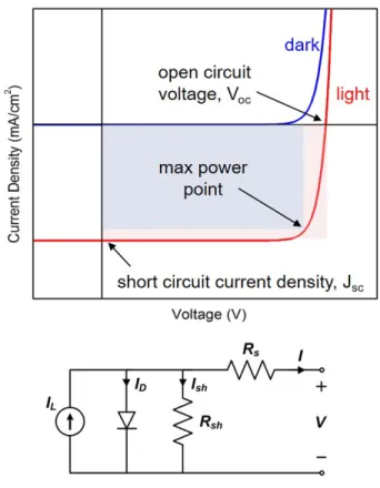
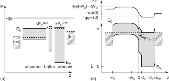
The open circuit voltage (VOC) is related to the band gaps between the n- and p-type materials as well as the quality of the interface. The short-circuit current (JSC) is a measure of the photocurrent collected by the solar cell.
Motivation for Cu 2 O photovoltaics
Energy band alignment
To maximize the open circuit voltage of the device, the conduction band of the buffer layer should be slightly above the conduction band of Cu2O, so that ∆EC is approx. 0.3 eV or less. In the case of the valence band offset, ∆EV, we want the valence band of Cu2O to sit much higher than the buffer's valence band, which will block holes from moving into the buffer and causing recombination.
Scope of this thesis
First devices incorporating MBE-grown Cu2O absorber: We conclude Chapter 5 by fabricating and analyzing the first Cu2O/Zn(O,S) solar cells made using molecular beam epitaxy to grow the Cu2O absorber layer . Appendices: Oxide MBE and PLD User Guides: Much of my time has been spent using, fixing and maintaining the oxide molecular beam epitaxy and the pulsed laser deposition systems.
Introduction to Molecular Beam Epitaxy
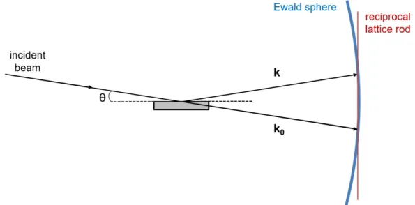
Reflection high energy electron diffraction
The diffracted intensity is seen when the reciprocal grating of the surface material crosses the Ewald sphere. In addition, there may be a broadening of the Ewald sphere itself as a result of energy variations in the electron beam.
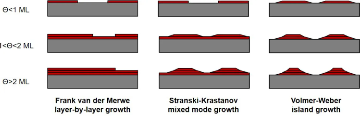
Thin film growth modes
The stripes will be shortened by the presence of a non-zero cutoff of the sample surface or atomic steps on the surface, with larger steps producing longer stripes. This typically occurs due to a change in energetics beyond a critical layer thickness, which is related to the film's chemical potential as well as strain.
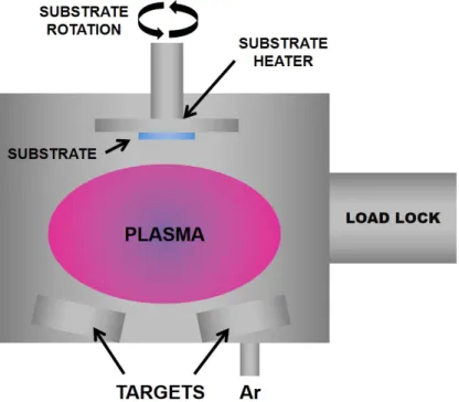
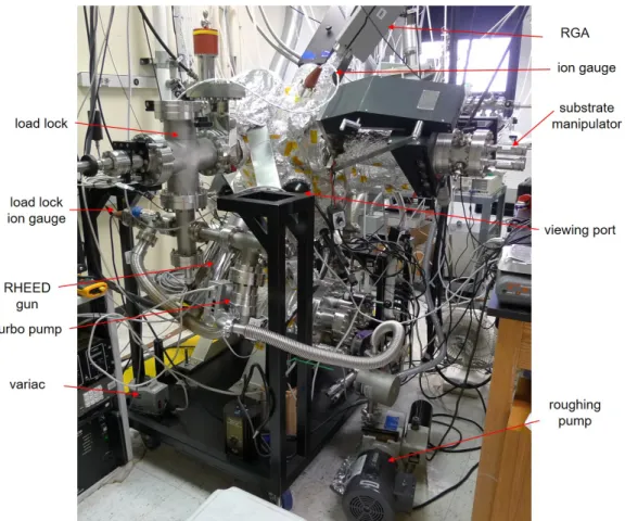
Experimental Setup
Ionic components of the plasma escaping the atom source were further filtered out by ion deflection plates. The presence of argon enabled the stability of the plasma, while lowering the partial pressure of reactive oxygen species.
Growth using pure oxygen plasma
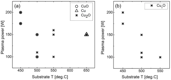
Growth of Cu2O begins with islands corresponding to two symmetrically equivalent variants of the Cu2O (1 1 0) surface so that the pattern in Figure 2.6 (b) is a superposition of the Cu2O [1 1 1] and [2 1 1] zone- as are transfer patterns. The substrate temperature is already approaching the limits of the system, and higher growth temperature is generally undesirable in terms of substrate compatibility and cost.
![Figure 2.6: RHEED images of Cu 2 O growth on MgO using pure oxygen plasma. (a) Plasma cleaned MgO (1 0 0) surface along the [1 1 0] azimuth, (b) 100 nm of Cu 2 O showing growth initiates and persists in the Volmer-Weber or island regime and the pattern is](https://thumb-ap.123doks.com/thumbv2/123dok/10416540.0/30.918.174.757.552.797/figure-plasma-cleaned-surface-azimuth-showing-initiates-persists.webp)
Growth using 90%Ar/10%O 2 plasma
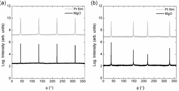
Looking at the [1 1 1] Cu2O azimuth in Figure 2.9 (e), all spots can be indexed according to the corresponding transmission diffraction pattern shown in Figure 2.9 (f), and no additional spots corresponding to the [2 1 1] azimuth displayed. gift. The selected area diffraction pattern in Figure 5.5(b) shows that the Cu2O lattice directly overlaps the MgO lattice and the film appears stretched.
Metal Films on Dielectric Substrates
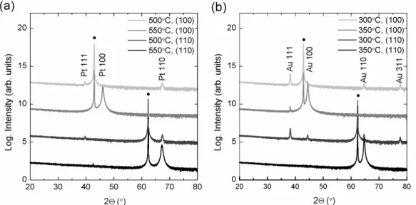
Nucleation and growth of Pt and Au particles on MgO is the subject of intense study, and reviews exist on the subject [37]. Fewer studies of Au thin film growth on MgO exist [42], although nucleation of Au particles has been extensively studied. In this report, we show that substrate bias facilitates epitaxial growth of Pt and Au films on MgO by increasing the mobility of surface adatoms, affecting the number and density of nucleation sites, increasing film density, and disrupting columnar grain growth.
Bias-assisted sputtering
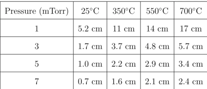
To understand the particle energies involved in sputtering, it is useful to look at the mean free path (λ), or the average distance a particle travels before it collides. The mean free path at different temperatures and pressures relevant to this study is shown in Table 3.1. The mean free path is therefore greater than the width of the dark space over which the plasma is non-neutral and the electric field is greatest, which has been measured to be about 3 cm.
Growth of Pt and Au on MgO by Bias- Assisted SputteringAssisted Sputtering
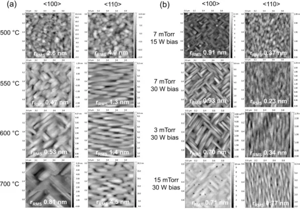
In order to try to reduce the roughness of Pt films grown on MgO(1 1 0), we adjusted the working pressure and substrate bias by keeping the substrate temperature at 550◦C, which was the lowest temperature at which epitaxy occurs for the given growth rate. In contrast, increasing the operating pressure while maintaining the same substrate bias results in smaller grains due to a greater number of nucleation sites for the film and a decrease in the energy of the atoms striking the surface. In addition, we illustrate the effects of varying the size of the substrate bias and the operating pressure on the device morphology.
O Growth on
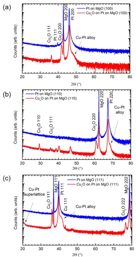
As we will show, the stability window of the Cu2O phase must be reoptimized for each substrate orientation. Cu2O growth starts in the island growth mode as evidenced by the patchy nature of the RHEED pattern at a thickness of about 5 nm. High-resolution TEM micrographs of (a) the Pt/MgO interface and (b) the Pt/Cu2O interface are shown in Figure 4.6.
O Device Synthesis and Characterization
Device Preparation Scheme
The thickness of the Cu foil was 0.5 mm and the final thickness of the Cu2O wafers was about 0.8 mm, with a typical carrier concentration of 1013-1014 cm-3 and a hole mobility of about 65 cm2V-1s-1. A Zn(O,S) layer approximately 40 nm thick was co-sputtered from ZnO and ZnS targets of 4N purity at an operating pressure of 5 mTorr Ar. A shadow mask was placed over the samples and a 60 nm ITO layer was then sputtered at 50 W in an Ar atmosphere at an operating pressure of 3 mTorr, without intentional heating.
Bulk Cu 2 O-Zn(O,S) devices
- Zn(O,S) as a Heterojunction Partner to Cu 2 O
- Current-voltage analysis
- External quantum efficiency characterization of solar cell deposited at 100 ◦ Csolar cell deposited at 100◦C
- XPS characterization of Zn(O,S)/Cu 2 O interfaces
- Structural Characterization of Zn(O,S)/Cu 2 O in- terfaceterface
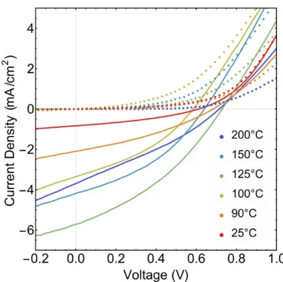
This reduction in the barrier may be due to photodoping of the Zn(O,S) buffer layer, which is confirmed by the spectral response in Figure 5.3. To check whether the presence of CuO on the surface affected the chemistry of the growing Zn(O,S) film and promoted sulfate formation, a Cu2O wafer was annealed at 200 ◦C to remove the CuO layer and then cooled to 100°C. ◦C before deposition of Zn(O,S). c), the concentration of sulfate in this sample is insignificantly different from the sample grown at 100 ◦C, suggesting that the presence of CuO on the surface does not significantly promote ZnSO4 formation and that the deposition temperature is the dominant factor to limit ZnSO4 at the interface. We report on the effect of deposition temperature on the composition of the Zn(O,S)/Cu2O interface and the resulting changes in solar cell performance.
LBIC characterization of polycrystalline Cu 2 O solar cells
- LBIC setup
- Electron backscatter diffraction
In addition, the higher resolution scans in Figure 5.8 (a-h) show the presence of surface dimples that act as current sinks. To investigate possible reasons for the grain dependence of photocurrent collection, the out-of-plane crystallographic orientation of the polycrystalline Cu2O wafers was mapped using EBSD, as shown in Figure 5.9. According to EBSD, the grain contributing the most photocurrent in Figure 5.9 has a (1 0 1) surface orientation.
![Figure 5.6: Schematic beam path of LBIC setup [image credit: Zeiss]](https://thumb-ap.123doks.com/thumbv2/123dok/10416540.0/74.918.261.660.119.493/figure-schematic-beam-lbic-setup-image-credit-zeiss.webp)
Thin Film Cu 2 O Devices
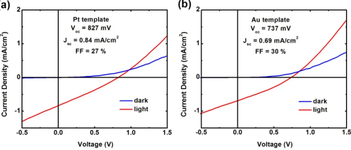
This thickness of Cu2O is not sufficient to absorb all the incident light, so we expect a decrease in performance compared to bulk polycrystalline wafers. First, we successfully demonstrated the epitaxy of Cu2O on single crystal MgO substrates with different crystallographic orientations. Second, there is an optimal orientation of Cu2O that would optimize the surface stoichiometry and solar cell efficiency.
Sample loading
First, move the loading arm magnet so that the chuck slides onto the main chamber fork assembly. When the chuck is fully loaded, use the rotation knob to rotate the main chamber fork clockwise. When rotation is no longer possible, tilt the assembly to release the chuck and carefully begin to pull the arm out.
General growth procedure
- Heating Cu source
- Heating substrate
- Plasma
- RHEED
When the reflected power has gone to zero, this is the low brightness state of the plasma (the plasma is not "illuminated"). When the plasma is bright, reduce the chamber pressure to the desired deposition pressure and slowly adjust the power. The optical emission voltage is the integrated optical emission of the plasma and contains information about the plasma efficiency.
Shutdown
If the RHEED is not used for less than 1 hour, the current and voltage can be maintained at 1.2 A/20 kV. Placing the substrate in the same position on the chuck is important for searching in RHEED and for obtaining reproducible deposits.
Notes and Troubleshooting
Bakeout
Cleaning and loading
Changing the height of the target can greatly change the focus of the laser and the rate/time of application. In the Target Motors Control panel on the left, press Home to start the target carousel. Check that the motors are working properly and stop them until you are ready to pre-ablate the target.
Pumpdown
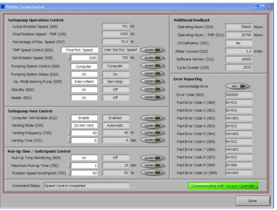
Amps and turbo should not be at maximum value for a long time. Please do not change any parameter in this window, use it only to monitor turbo power.
Pre-deposition
- Temperature Control
- Deposition pressure control
- Laser warm-up
Inspect the laser and system to ensure that the plastic beam path shield cage is closed and flush with the chamber and laser. Make sure the laser shutter is closed and the exhausts are connected and working properly. Make sure your laser safety glasses are on and the sample shutter is down and the laser shutter is closed.
Pre-ablation & deposition
The EGY PGR mode is only used for systems under continuous operation and here the laser will partially recharge automatically to maintain a constant power output. It is essential to warm up the laser first; this will ensure uniform pulse parameters. In the laser control window (Figure 6), execute 100 pulses with a frequency of 1 Hz; then run 100 pulses at 5Hz, and so on until you reach the desired pulse frequency and energy.
Annealing & Cooling Down
Venting
Disconnect the cables connected to the X and Y motors on the flange supporting the target carousel. Place your arm under the motors and one hand on the underside of the flange, gently push down on the flange to break vacuum and slowly remove the flange/carousel device. Be sure not to damage electrical ports and connections on the outside of the flange.
Note
When the pressure in the chamber reaches 700 Torr (see convectron gauge in Figure 1), close the vent valve so that you do not pressurize the chamber.
Laser Refill Procedure
Start the refill process where the mechanical pump will first pump the laser cavity and then refill it with a new buffer. If the filling does not stop automatically and the pressure no longer increases, press BREAK on the control panel. Purge” will evacuate the gas in the line using the vacuum pump and then refill the line with inert gas (He).
LN2 tank
Molecular beam epitaxy growth of CuO and Cu2O films with control of oxygen content by Cu/O+ flow ratio. Epitaxial growth of Cu2O and ZnO/Cu2O thin films on MgO by plasma-assisted molecular beam epitaxy. Growth of single-crystal Cu2O (111) film on MgO-modified α-Al2O3 (0001) ultrathin substrate by molecular beam epitaxy.
![Figure 2.9: RHEED images of Cu 2 O growth on MgO using argon-oxygen plasma. (a) Plasma cleaned MgO (1 0 0) surface along the [1 1 0] azimuth, (b) 60 nm of Cu 2 O proceeds with island growth shown here along the [1 0 0]](https://thumb-ap.123doks.com/thumbv2/123dok/10416540.0/34.918.168.753.115.358/figure-rheed-images-plasma-cleaned-surface-azimuth-proceeds.webp)