Realizing the effects of strain in the model makes it possible to understand the physical properties of strained layered superlattices, for example, optical properties and transport phenomena, both of which are functions of the band structure. In the thin film limit, the magnetic effect in the superlattice is found to be exactly that of an alloy corresponding in composition to the superlattice.
Introduction
The superlattice has a band gap that varies from zero to the band gap of CdTe depending on the layer thickness. In this method, the bandgap and the optical array element of the constituent materials are input parameters that can be detected.

Superlattice k ∙ p Theory
Having illustrated the basic principles involved in superlatticek∙p theory, we now address the question regarding the variation in Bloch functions. The difference in Bloch functions for the constituent materials can be attributed to the difference in their crystal potentials.
II-VI superlattices
The bandgap of this system can be tuned by varying the layer thickness and by applying a magnetic field. In Section 5, we discuss the magnetic field tunability of the band gap for the Hg1-ζcMnxTe∕Cdι^yMnyTe superlattice.
GaAs/AlAs Tunnel Structures
The transmission is proportional to the overlap in the barrier wave functions of the initial and the final conditions in the tunneling process. In Chapter 6, we will use the Hamiltonian transfer method to analyze phonon-assisted tunneling and illustrate the importance of inelastic tunneling in the double barrier problem.

Summary of Thesis
Background
Joint density of states per unit volume is, in the approximation, given by (score of spin degeneracy). The inclusion of strain effects in the theory of superlattice band structures is very important.
Outline of the Chapter
However, a theory that can predict the critical thickness of a strained-layer superlattice has not been satisfactorily developed. The theory developed here is able to predict the effects of voltage on electronic properties.
First-Order Theory
Outline of First-Order Theory
Strained Crystal Band Structures
In other words, the elastic energy of the system is minimized with respect to the lateral lattice constant (i.e., the transverse force on the superlattice is zero) while subject to the constraint that the normal force on each interface is zero. The zero energy is considered to be at the valence band edge of the unstrained CdTe. The superlattice valence band edge is determined by the higher one of the heavy hole and light hole subbands.
In the case that the subband of the light holes is higher, the gap is equal to the energy difference between the edges of the conduction and the subbands of the light holes. This explains why in Figure (2.3) and Figure (2.4) the band gap changes relatively quickly with the number of CdTe layers, while it changes relatively slowly with the number of ZnTe layers. It allows us to associate to each eigenstate a wave vector Q in the direction of superlattice growth.

Electron Wave Function in a Single Material
However, to use this wave function in the superlattice problem, we need to investigate whether extra field is produced by magnetization in the superlattice. In the problem, the magnetic field in a layer is uniform and perpendicular to the layer. In other words, magnetization in one layer does not affect electronic motion in other layers.
Boundary Conditions at Interfaces
Since the superlattice structure preserves translational symmetry in the x direction, kx is a quantum number. To calculate the matrix ∫dy'o{d'k^inl\jz{ro)\dk^,^A, we simply put the last term in Eq. The boundary condition expressed using current density matrices only couples bulk states with the same n, as indicated by the δ function in Eq.
Following the same procedure as in Chapter 2, we calculate the current density at the interface and obtain.
Bloch Condition for a Superlattice Wave Function
Superlattice Eigenvalue Equation
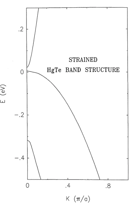
In section (4.3), we present the band gap and optical properties of the HgTe-CdTe superlattice as functions of the valence band offset. The CdTe substrates result in the greatest strain on the HgTe layers of the superlattice. As shown on the right of figure (4.8), the band structure for the strained superlattice shares some common features with the unstrained one.
Figure 4.9: The band structure at zero fc∣∣ for the (111) superlattice consisting of alternating layers of 70.6Â HgTe and 70.6Â CdTe. However, if the valence band offset is positive (that is, the valence band edge of Cd0.8Mn0.2Te is higher than that of Cdo.7Mno.3Te) and not close to zero, then the gaps are more likely to be confined to Cd0 .eMn0.2To layers. On the other hand, if the valence band offset were negative (that is, the valence band edge of Cdo.8Mno.2Te is lower than that of Cdo.7Mno.3Te) and not close to zero, then the gaps would be limited to Cdo.7Mno.3Te. layers.
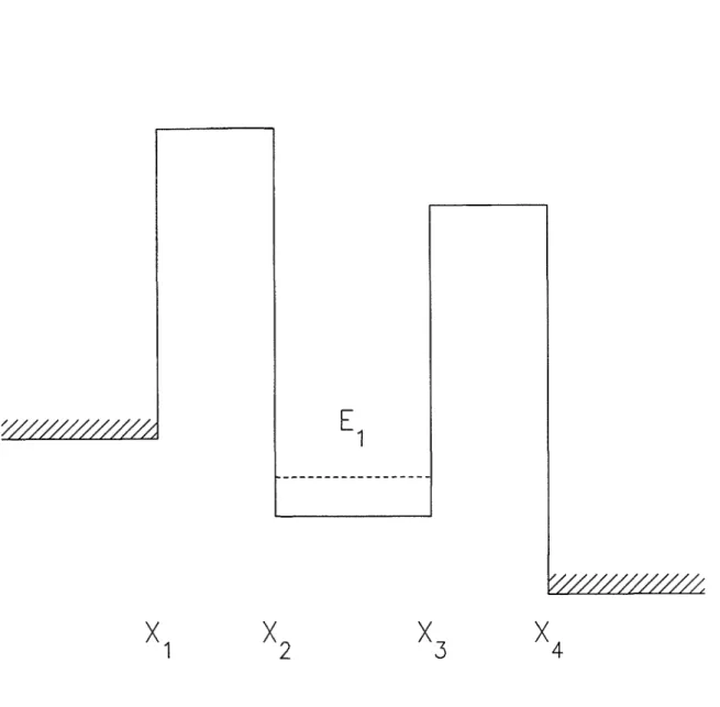
Note that according to equation 6.4), the ratio of on-resonance transmission to off-resonance transmission is . In figure (6.4) the upper limit of the ratio is plotted against the Fermi energy for a symmetric structure with d = 40 Â and w = 50 Â.

Examples of Semimagnetic Semiconductor Superlattice Band Struc
Summary
On the other hand, in the case of superlattice, the band gap is controlled by the thicknesses of the HgTe and CdTe layers. However, the dielectric function depends on the superlattice band structure which in turn depends on the value of the valence band offset. Thus, the value of the valence band offset can be any number from 0 to 0.5eV.
In section (4.4) we present a study of strain effects on the band structure, band gap and optical properties of the HgTe-CdTe superlattice at zero temperature.
Optical Properties of the HgTe/CdTe Superlattice
- Dielectric Function
- Band Structures of HgTe, CdTe and HgCdTe
- Band Structure of a HgTe/CdTe Superlattice
- Comparison of Superlattices and Alloys
If we assume that the matrix element is a smooth function of k, then in the previous equation we can factor the matrix element from the integral and get The valence band edges are conditionally aligned to reflect the smallness of the valence band offset. An important result of this calculation is that the magnitude of e2(ω) for the superlattice is comparable to that of the alloy.
But in fact we do not fully know the imaginary part of the dielectric function.

Band Offset and Optical Properties
Strain Effects and Optical Properties
The effective masses of the electron and hole are about 0.002me, and the effective mass of the heavy hole is about 2me for the motion perpendicular to the layer. We have also studied the band structure of the (001) strained superlattice of the same composition. Consequently, the effective masses of the subbands occur in different order in the two cases.
For a (001) superlattice of the same composition, the band gap is 95 meV, and the two valence subbands are separated by 12 meV.
Summary
Optical Properties
Band Offset Effects
At negative bias, the electron and hole are separated and the rate of radiative recombination is reduced.
Strain Effects
Chow og D.Johnson, Proceedings ofthe1984 Workshop on the Physics and Chemistry of Mercury Cadmium Telluride, J.
Semimagnetic Semiconductors
In magnetic semiconductors, the strongly interacting system of magnetic ions is in a magnetic state and does not respond to the external magnetic field. Both the decrease in temperature and the increase in the magnetic field result in an enhancement of the spin polarization (Sz}. The theory that describes in detail the motion of an electron in a magnetic field is described in Chapter 3.
As the intensity of the magnetic field increases, the magnetic spins align and saturate at some point.
Semimagnetic Superlattices
The energy of the stimulated emission peak is shifted by the application of a magnetic field. The band product is due to the exchange interaction of the band electrons with the 3d localized electrons in Mn++. For the case of B = 5 and zero spin temperature, much larger separations occur, due to the exchange interaction, and the superlattice band gap is reduced by the magnetic field.
Bandwidth derivations with magnetic field at low magnetic field are also shown. The width of the resonance is inversely proportional to the lifetime the electron remains in the cavity. In summary, the inclusion of inelastic tunneling in the theory for double barrier structures is very important.

Summary
In the wide-gap system, the valence band shift was chosen in accordance with the experiments. The change in the band gap at low field is found to decrease with the displacement varying from negative to positive value, since the hole confinement site changes from Cdo.7sMno.22Te to Hgo.95Mno.o5Te layer. In the self-consistent analysis, Ohnishi et al have included the Hartree potential in the calculation of resonant tunnel current5.
But in the recent study of GaAs-AlAs-GaAs structure, Collins, Lambe and McGill6 reported the observation of inelastic tunneling of electrons.

Theory of Elastic Tunneling
In this chapter, we present the first theoretical study of the effects on the tunneling current in a double-barrier structure due to the electron-phonon interaction. The Hamiltonian transfer method, originally proposed by Bardeen7 to treat electron tunneling through a single-barrier structure, is extended to calculate phonon-induced inelastic tunneling in a double-barrier structure. It shows how quickly the transmission drops as the energy of the incident electron deviates from the energy of the quasi-bound level.
On the other hand, when the bias is outside the resonance value, setting Eq. 6.11), we get the ratio of the peak value to the valley value.
Theory of Inelastic Tunneling
Electron-phonon coupling in the left barrier of AlAs results in an interaction Hamiltonian. Here, Dγ is the strain potential for Γ-valley electrons, p is the density, υa is the speed of sound in AlAs, and VAiAa is the volume of the left barrier. Suppose the electron is now scattered to a quasi-bound level, then ≠r in the left barrier would increase by an exponential factor of eli2d2.
Therefore, the contribution to the inelastic current for such a process will dominate over others without taking the resonant level in the tunnel.
Comparison of Elastic and Inelastic Tunneling
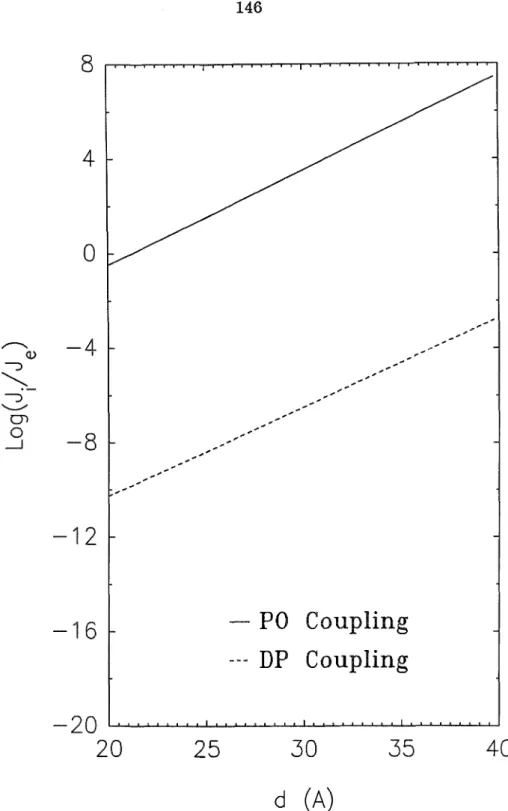
In figure (6.3), we show the upper limit of the ratio of the resonant current that occurs at Va = 0.3 V and the current at Va = 0.4 V that occurs outside of resonance, depending on the thickness of the barrier. In this case, the relationship shown here is the same as the relationship between the peak and the trough of the J-V curve. The off-resonance current is largely due to inelastic tunneling, since the inelastic current is much larger than the elastic current, as shown in Figure (6.2).
The solid curve includes contributions from the inelastic process, and the dashed curve includes only contributions from the elastic process.
Summary
We also provide Hamiltonian matrix and current density matrices involved in the calculation of band structures of semimagnetic semiconductor superlattices.
Derivation of Effective-Mass Equation
Basic functions for perturbation calculation are considered as the eigenstates Uβ of the reference Hamiltonian Hr at k = 0, i.e. The derivation of the effective mass equation for fβ{r} requires lengthy manipulations. A.6) by integrating Uβ>(r)eik'∙f, and then over the entire space, a series of simultaneous equations is obtained. We will then reduce the dimension of the above simultaneous equations in the spirit of Löwdin perturbation theory.
We now look for solutions consisting mostly of the d-states, i.e. those containing Cdfd(r),s as zeroth-order terms and Cafa(r)s as first-order terms.
Hamiltonian matrix
Unfortunately, the symbol "B" here, in accordance with convention, denotes a second-order perturbation matrix element rather than the magnetic field.
Current Density Matrices
In this appendix we derive the expression for inelastic tunneling current in a GaAs-AlAs-GaAs-AlAs-GaAs structure.
Derivation
For cases where the assumption that ki)dι is small does not apply, the approximation underestimates the value of ∣Γ∣2 and consequently Ji∙n. In calculating the integral of jin, κ,τ is estimated by expanding κ,ι and rer around the zero energies of the two electrodes. Eb — eVα∕4 for the left barrier and Eb∙,R = Eb + eVa∣⅛ for the right barrier, for a symmetric structure with zero barrier height bias Eb. B.ll).
The integral over dφ on the right side of the inequality can be evaluated analytically and results in a function G(fc∣∣, ⅛∣∣.


