With the rapid growth of the semiconductor industry, channel lengths in chips have decreased drastically in recent years. This is the first measurement of the band gap at the Si-ZrSiOx interface using any technique. Although today amorphous silicon (a-Si) is a promising material for photovoltaic devices, crystalline silicon (c-Si) is undoubtedly the primary focus of research activity as it represents the foundation of the semiconductor industry.
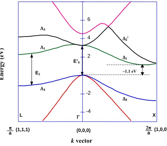
It is almost degenerate with the E1 transition of about 3.37 eV (Figure 1.2), which is found along the Λ direction of the Brillouin Zone (BZ). The second is the extremely high quality of both the interface and bulk properties of the SiO2 passivation layer.
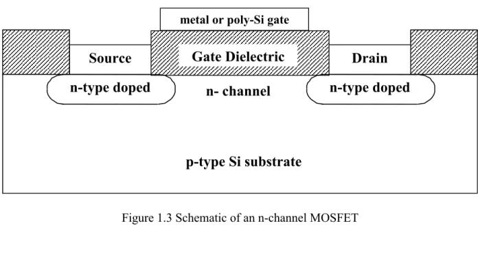
Gate Dielectric Drain Source
As a passivation layer, it allows stable and predictable conditions at the semiconductor surfaces/interfaces to be produced during processing. More importantly, an ideal barrier insulator should have a large dielectric constant, low trap density at the interface, and a low density of bulk fixed charges. But in the last ten years, the semiconductor technology has grown rapidly and new challenges are emerging.
This, in turn, requires the gate oxide thickness to be reduced to 30 Å, ultimately to less than 10 Å. As a result, diffusion of the dopant (boron) into and through the SiO2 layer from the poly-Si gate metal or poly-Si gate.
A Review of Second Harmonic Generation (SHG)
The sum of the electric dipole moments results in polarization (P) of the material. The motion of the ions is insignificant compared to the motion of the much lighter electrons. However, if the light intensity is high, the electromagnetic field will be large.
The following year, Heinz showed that the azimuthal dependence of the SHG signal was sensitive to the symmetry change between the (2x1) and the (7x7) reconstructions of the Si (111) surface. Since second harmonic generation is a nonlinear optical process, it strongly depends on the intensity of the excitation source.
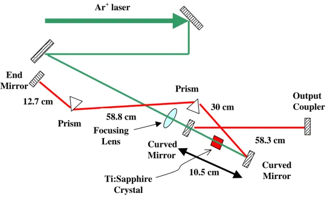
The Construction of a Ti: Sapphire Laser
- Theory of operation
- Characterization of Ti:Sapphire Lasers
- Mira 900 Ti:Sapphire laser
The success of the Ti:Sapphire laser in achieving short pulse widths arises from the application of the mode-locking technique. Once the pulse is formed, the subsequent persistence of the pulse depends on two phenomena. When a pulse propagates in a medium, its group velocity can vary according to the frequency distribution of the pulse.
Unfortunately, the remaining terms on the right side of (2-9b) show a phase modulation of the frequency spectrum. Although the prisms and optical materials in the cavity determine the overall dispersion, SPM depends on the intensity of the pulse. The dimensions shown in Figure 2.4 have different roles and importance in the operation of the Ti:sapphire laser.
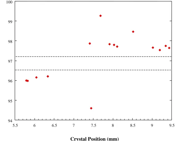
The separation between the two curved mirrors and the position of the crystal are very critical. A systematic measurement of the mode-lock stability as a function of mirror separation and crystal position is shown in Figure 2.5. But when combined with spectroscopic measurements, second-order autocorrelation can still reveal much of the pulse structure.
Following the convention of using ν, which is ω/(2π), the product of these two, called the time-bandwidth product, is a constant equal to 2ln2/π. Therefore, a measurement of the bandwidth product of a given pulse reveals how close the pulse is to the limiting case of the Fourier transform. But as shown earlier, the positions of the prisms have significant effects on the pulse width.
Therefore, its pulse width is also affected when the wavelength of the Ti:sapphire laser is changed. This results in a change in the polarization of the beam when these two components recombine.
Experimental Setup
More importantly, since the tunability is achieved through the birefringent filter instead of a prism, the pulse width can be maintained the same.
Rotation TableSample
Lenses
Iris
Electric Field Induced Second Harmonic Generation (EFISH)
Lee, 1967] This effect was later also discovered from other centrosymmetric materials and led to a new field of SHG research called electric field induced second harmonic generation (EFISH). Pi(2ωωωω)====χχχχijk(3)Ej(ωωωω)Ek(ωωωω)Edc (3-1) where χ(3) is a third-order bulk susceptibility with electric dipole origin. As discussed earlier, electric dipolar contribution to SHG in centrosymmetric materials is forbidden in the main case.
But when an electric field is applied to the bulk, it breaks the inversion symmetry and allows SHG contributions from the bulk electric dipole. Since the bulk susceptibility is third order, this electric-dipole-origin SHG is smaller than the bulk electric-dipole contribution of composite materials such as GaAs. But when the quasi-static field Edc is high enough, this SHG signal can be comparable to or even higher than that of the surface with dipolar origin and that of the bulk with magnetic dipole and electric quadrupole origins.
An externally applied voltage, as in the original work, is the most straightforward way to generate this quasi-static field. Since most semiconductor devices require an external voltage during their operation, EFISH can be an excellent tool for in situ investigation of device performance. Aktsipetrov 1984] [Aktsipetrov 1996] Since the dc electric field varies along the penetration depth of SHG radiation zp, a more rigorous expression for the nonlinear PBD polarization induced by the electric field is of the form
Pi(2oooh)====ххххijk(3)Ej(oooh)Ek(oooh) Eòòòò dc(z)dz (3-2) όπου η ολοκλήρωση λαμβάνεται πάνω από το βάθος διείσδυσης zp. Αυτό σημαίνει ότι η πραγματική κατανομή πεδίου Edc(z) στο SCR μπορεί να αντικατασταθεί από μια σταθερή Eint μέσα σε ένα στρώμα ενεργού μήκους z0 που είναι συγκρίσιμο με το πλάτος SCR. P(2yyyy) ====x x x x JBQ : E(yyyyyy)∇∇∇E(∇yyyy) +yyyyyy JSD : E(yyyyyy)E(yyyyyy)dddd(0) +yyyyyy JBD : E(oooooooo)E(oooooooo) ) ) Edc (3-3) όπου οι δύο πρώτοι όροι στα δεξιά αντιπροσωπεύουν αντίστοιχα τη συνεισφορά μάζας της αρχής μαγνητικού διπόλου/ηλεκτρικού τετραπόλου και τη συνεισφορά στην επιφάνεια της αρχής ηλεκτρικού διπόλου.
Results and Discussion
- Sample Preparation and Experimental Method
- SHG from Si/SiO 2 system
- An overview of Si-ZrSiO x system
- SHG from Si/ZrSiO x system
When the photon energy of the Hg lamp is greater than 4.38 eV, an SHG feature similar to that in Figure 3.1 is observed. Figure 3.3 shows the first definitive evidence of a three-photon process between the conduction bands of silicon and silicon dioxide. While the photon energy decreases to about 1.38 eV (9000 Å), well below the 1.47 eV threshold for a three-photon process between the silicon valence band and the oxide conduction band, second harmonic signals still exist.
The SHG signals gradually increase as the photon energy increases from about 1.35 eV to 1.55 eV. Second, it is well known that there is a resonant peak at about 3.4 eV in the SHG spectrum versus the photon energy of silicon. This resonance also leads to a strong enhancement of SHG signals in the photon energy range above 1.5 eV.
Due to the multiphoton injection of electrons, the static field Edc in equation (3-4) will increase with increasing photon energy. On the other hand, due to the direct resonance of the band transition, the nonlinear susceptibilities, χ(2) and χ(3), in equation (3-4) also increase with increasing photon energy. However, the appearance of time-dependent SHG below 1.47 eV in Fig. 3.3 constitutes a clear evidence of the three-photon process between the conduction bands of silicon and silicon dioxide.
When light is present, with sufficient photon energy to inject electrons into the oxide, this capture process is greatly enhanced. There is clearly an abrupt change in the initial rise at a photon energy of about 1.4 eV. But when the photon energy is lower than 1.4 eV, the initial rise is no longer observable.
Time (sec)
Thermal effect in SHG from Si/ZrSiO x system
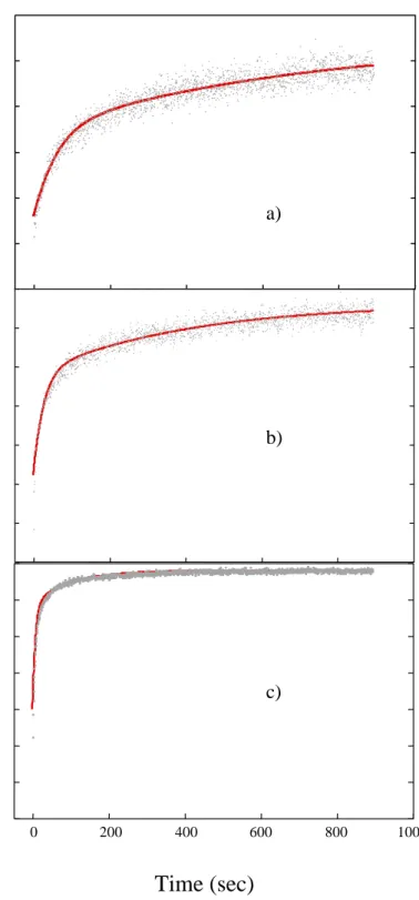
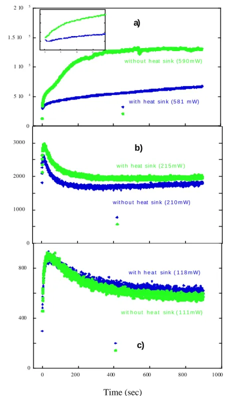
Compared to those with lower power, a third process has emerged which leads to a gradual but significant increase in SHG. At very high power, this process totally dominates other processes which are of electronic origin (Fig. 3.12a). At 500 mW power, a measurement of the temperature on the back of the sample shows an increase of 30°C in less than 1 minute.
To eliminate this effect, the sample is mounted on a large aluminum block, which acts as a heat sink. The significant increase in SHG signals observed when there is no thermal insulation has been. The decrease in SHG also reappears even at very high power as shown in the inset in Fig. 3.12a.).
This strongly indicates that at high laser incident intensity, the monotonous increase in the SHG signal throughout the measurement time is due to the gradual increase in sample temperature caused by the incident laser. As the laser power decreases, this effect becomes less pronounced. It has essentially no effect at low power (Figure 3.12c), which is the power range used in the previous measurements.
Dadap 1995] It is believed to be due to thermoelastic deformation arising from differences in the rates of thermal expansion of the oxide layer and the substrate. The deformation normal to the surface creates a local structural gradient at the Si-SiO2 interface, which acts as additional sources of nonlinear polarization. In our experiments, since the physical thickness of the ZrSiOx layer is much larger than the ultrathin SiO2 layer, the stress induced by the thermal expansion difference is also much larger, which then dominates the SHG signals.
SiZr
- Summary
- Ongoing Work and Future Plan
- Classical Harmonic Oscillator (Lorentz Model)
- Nonlinear Susceptibility of a Classical Anharmonic Oscillator
- Centrosymmetric Materials
This thesis describes research into the application of intense, tunable, ultrafast lasers to studies of the silicon dielectric system. In the Si-SiO2 system we show the first definitive evidence for the electron injection of three photons from the silicon conduction band to the silicon dioxide conduction band. Our data shows characteristics drastically different from those of the Si-SiO2 system.
This thesis illustrates the successful use of the SHG technique to study both Si-SiO2 and Si-ZrSiOx systems. In Si-ZrSiOx system, the compositions of SiO2 and ZrO2 affect many properties of the system, including the band gap of ZrSIOx and the band deposits at the Si/ZrSIOx interface. The classical Lorentz model of the atom, which treats the atom as a harmonic oscillator, has been proven to be successful in describing linear optical properties such as dispersion and resonance absorption.
Therefore, it cannot describe the full resonant nature of nonlinear susceptibility, such as the possibility of simultaneous one- and two-photon resonance. In contrast, the quantum mechanical theory of nonlinear optical susceptibility can adequately address such issues. When the incident electromagnetic field is large, the displacements of the electrons from their equilibrium positions can be large enough that the potential felt by the electrons deviates from the function of the parabola.
If the deviation in the displacement x(t) is small, only terms up to the third power of E(t) need to be considered. And if (A-11) holds for all fields, terms with the same power of E(t) must be equal on both sides of the equator. Following the definition of polarization in (A-6), one finds the expression for the second-order nonlinear term of the polarization.
![Table 1.1 Some important properties of metal oxides. After [Feldman 1998]](https://thumb-ap.123doks.com/thumbv2/123dok/10740626.0/16.1188.111.1079.217.756/table-some-important-properties-metal-oxides-after-feldman.webp)