To Jack Beauchamp and Bruce Brunschwig, thank you for all your time spent in meetings and for all the valuable feedback given on my exam timeline and thesis work. Kim, thank you so much for all the roles you've played during my time here - adviser, editor, counselor and friend. Bruce, thank you for always being so invested and involved in the group's work.
Thank you for advocating for us and being such an integral part of the Lewis Group. Thanks to all the undergraduates, graduate students, and PhD students I've worked with since coming to Caltech - I apologize if any of you are not specifically mentioned. First, Azhar Carim, thanks for being one of the first members of the Lewis group I met during my weekend visit and helping me find my first project, even though the "trees" are still out of reach.
Influence of Substrates on the Long-Range Order of
Introduction
Results and Discussion
- Matched-illumination growth conditions
- Nucleation dynamics
- Junction analysis
- Matched deposition-rate conditions
Conclusion
Supporting Information
- Experimental methods and materials
- Low-magnification SEM images used for FT analysis in Figure 1.1
- Additional data gathered for Se-Te films deposited on n+-Si and
- Results and data gathered for Se-Te films deposited on Au and
- Low-magnification SEM images of Se-Te films on p+-Si in Figure 1.5
- Nucleation density and growth substrate discussions
- Table with additional information for all samples fabricated
Increased Spatial Randomness and Disorder of Nucleates in
Introduction
Results and Discussion
Conclusion
Supporting Information
- Experimental methods and materials
- Examples of low-magnification images
- Reproducibility
- Pair-correlation function (PCF) examples
- Peak-fitting methodologies
- Schemes for phototropic growth mechanism
- Electron dispersive X-ray spectroscopy (EDS) compositional analysis
- Graphical representation of striking potential
- Dark growth during Se-Te electrodeposition on n + -Si
- Summary of previous phototropic growth studies
- Se-Te on Au substrates
Pre-seeded Optical Scatterers as a Template for Phototropic Growth
Introduction
Selective and directed growth of materials can be enabled by physical or chemical templating to yield anisotropy in morphology and function. For example, in a process similar to nanosphere lithography1, selective through-pore electrodeposition of zirconium can be achieved by physically blocking electrolyte contact at an otherwise conductive working electrode surface via a colloidal monolayer of polystyrene beads.2 Chemical functionalization can also ' provide a way. for variation in conductivity and reactivity across a substrate, which can be achieved by soft lithography3 or microcontact printing.4 In contrast to physically blocked or chemically modified surfaces, electrodeposition of metals can be selectively directed onto silicon microstructures due to work function, band conduction, and lighting conditions.5 Similarly, electrical contacts of nickel can be selectively deposited on silicon nanowires, seeded by Au electrodes.6. Pre-seeding growth substrates can also improve performance or ensure proper development of deposited films.
Epitaxial growth of GaN requires preseeding of aluminum on silicon prior to nitriding7-8 and the epitaxial growth of PbTiO3 on LaAlO3 is much improved by preseeding with Pb-Ti double alkoxide.9 Diamond films formed on silicon substrates via chemical vapor deposition in microwave plasma (MPCVD) demonstrate improved emission flux when substrates are pre-seeded. In a mild hydrothermal process, preseeding substrates with ZnO particles led to an increase in the aspect ratio of epitaxially grown ZnO nanorods.14-16 The development of anisotropy in a material can also be controlled by chemical templates that can facilitate facet-selective growth reaching or etching, especially in crystalline material. Unlike the nanowires normally obtained from the die-assisted electrodeposition of nickel, boric acid incorporation leads to the formation of nickel nanotubes.17 In the presence of chemical additives such as sodium dodecyl sulfate (SDS) or copper nitrate, electrodeposition exhibits cuprous oxide facet-selective growth during bottom- up synthesis.18 In a top-down etching procedure, Au microcrystals can be selectively etched in the (100) or (111) direction with silver tetraoctylammonium bromide (AgToABr) or Cu(Cl) 2. .19, respectively.
Mass availability,20-21 pH,22 growth kinetics23 heat flux,24 local light absorption,25-26 applied deposition potential during electrodeposition,18,27 and other conditions can also cause anisotropy in developing materials. We recently described the phototropic growth phenomenon in which highly anisotropic lamellae are formed from Se-Te,28-33 PbTe,34 and CdSe35 as a result of local light absorption during photoelectrochemical deposition. Phototropic growth of these semiconducting materials occurs via a one-step process that does not involve chemical or physical templates.
The lamellar morphology is formed spontaneously and there is no requirement for coherence of the optical input. Optical modeling and simulations of the phototropic growth process have shown that the high aspect ratio lamellae formed in phototropically grown films are a result of a feedback loop initiated by incident light scattered from an initially dark and isotropic distribution of core particles . This optical dipole scattering leads to localized light absorption in the tips of the emerging lamellae, leading to an equilibrium lamellar morphology.
However, phototropically grown films can demonstrate low pattern fidelity and an apparent limit to the "straightness" of lamellar features.32 Here we explore the effect of pre-seeded optical scattering (in the form of a physically templated substrate ) on the phototropic growth process and the fidelity, period, and orientation of the resulting patterns.
Results and Discussion
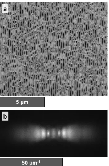
Thus, in Figure 3.1b, the features in the 2D FT spectrum correspond to orientation and period. In contrast to Figure 3.1b, the features in the 2D FT in Figure 3.2 are constrained vertically, indicating more vertically aligned and much flatter features on the template. The discontinuity and regular waviness of the lamellar morphology in Fig. 3.1a contribute to the significant broadening of the features in the 2D FT in Fig. 3.1b.
The film shown in the SEM image in Figure 3.3d corresponds to an unpatterned area that is optically isolated (distance ≫ 10 λ) and. 2D FT spectra in Figure 3.3e-h were generated from large area SEM images of the films in Figure 3.3a-d, respectively. The SEM images and 2D FT spectra in Figure 3.3 illustrate the increased pattern fidelity that physically annealed substrates induce on phototropically grown Se-Te films compared to untemplated substrates.
The high fidelity of the films is also demonstrated by the extremely sharp features in the 2D FT spectra in Figure 3.3e and f. The film in Figure 3.3c is slightly defective with some discontinuities and ramifications of lamellar morphology. The damaged nature of the film is also revealed in the enhanced and lower definition of the features in the 2D FT spectrum in Figure 3.3g.
Nevertheless, all phototropically grown templated films showed improved fidelity compared to the untemplated film in Figure 3.3d. The 2D FT spectra of the templated films also showed very defined and localized features compared to the relatively broad peaks observed in Figure 3.3h. The results of 2D FT analysis performed on phototropically grown films deposited on patterned and unpatterned substrates, including those shown in Figures 3.2 and 3.3, are given in Figure 3.5.
In addition to the implementation of the period as suggested by the data in Figure 3.5-3.10, there were also modeled substrates. observed to enforce the orientation of phototropically grown patterns.
Conclusion
Notably, for some of the higher polarization shifts (i.e., 40° and 45°), the component of the film patterns aligned with the polarization axis was more accentuated in the absorption profiles (Figure 3.12h and i) than in simulated images (Figure 3.12c and d), demonstrating the contribution to the pattern orientation from the illumination polarization axis and its competition with the pattern orientation implemented by the templates. For the simulated film with a 50° offset, the absorption profile (Figure 3.12j) demonstrated increased peak absorption (relative to films at a 40° or 45° offset) at the tips of the lamellae. Although the pattern in Figure 3.12e showed no substantial influence or competition with the underlying template, the absorption intensity observed in Figure 12j was lower than that observed in Figure 3.12f or g.
This is likely due to the lower pattern fidelity associated decrease in resonance between scattered illumination intensity and absorbing material. For example, phototropically grown films on template substrates can demonstrate periods of at least ∼80–165% of the natural period under a given set of illumination conditions. Similarly, the orientation of phototropically grown films on template substrates can be enforced with an up to ~40° offset in the polarization axis to the template orientation.
In summary, the use of optical scatterers as templates during phototropic growth demonstrates high pattern fidelity and complex morphological modes otherwise inaccessible in the phototropic growth process.
Experimental Methods and Materials
Pt-coated n+-Si substrates used as working electrodes in Se-Te deposition were fabricated via electron beam evaporation of target metals on n+-Si wafers. To make ohmic contact with the n+-Si, 15 nm Ti was evaporated on the top (smooth) side of the n+-Si wafers. After lift-off, an additional 70 nm of Pt was deposited via electron beam evaporation to produce template substrates.
The wafer chips were then attached to the exposed wire of the electrode holders with silver paint. A three-electrode configuration with an Ir wire counter electrode and an Ag/AgCl reference electrode (3M NaCl, BASi RE-5B) was used for the electrochemical experiments. A 600 grit diffuser (Thorlabs DG20) was placed in front of the window of the electrochemical cell to create uniform intensity illumination falling on the working electrodes.
All scanning electron microscopy was performed using an FEI Nova NanoSEM 450 with an acceleration voltage of 5 kV. Gwyddion (gwyddion.net) was used to perform Fourier analysis on the large-area images (acquired at 6250 X). The growth of the photoelectrochemically deposited films was simulated with an iterative growth model in which electromagnetic simulations were first used to calculate the local photocarrier generation rates at the film surface.
In the first step, the light absorption profile under a linearly polarized, plane-wave illumination source was calculated using full-wave finite-difference time-domain (FDTD) simulations (“FDTD Solutions” software package, Lumerical) with periodic boundary conditions along the substrate interface. A value of n = 1.33 was used as the refractive index of the growth solution, regardless of wavelength.36 Film morphology simulations used the intensity-weighted average wavelengths, λavg, of the experimental sources. The illumination electric field vector was oriented at and 50° off normal from the orientation of the template pattern.
After the initial Monte Carlo simulation, the absorption of the new, structured film was then calculated in the same manner as for the initial planar film, and an additional Monte Carlo simulation of mass addition was performed.
Zhu, D.; Ming, L.; Huang, M.; Zhang, Z.; Huang, X., Seed-assisted growth of high-quality multi-crystalline silicon in directional solidification. Chen, H.-G.; Li, Z.-W.; Lian, H.-D., Control of epitaxial growth orientation in ZnO nanorods on c-level sapphire substrates. M.; Shen, M.; Zhao, T.; Sadtler, B., Light-driven, facet-selective transformation of copper oxide microcrystals to hollow copper nanoshells.
Morphological expression of coherence and relative phase of optical inputs in photoelectrodeposition of nanopatterned Se-Te films.