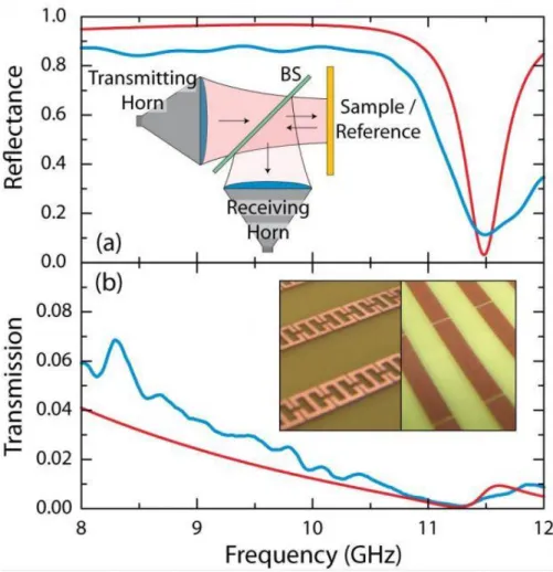
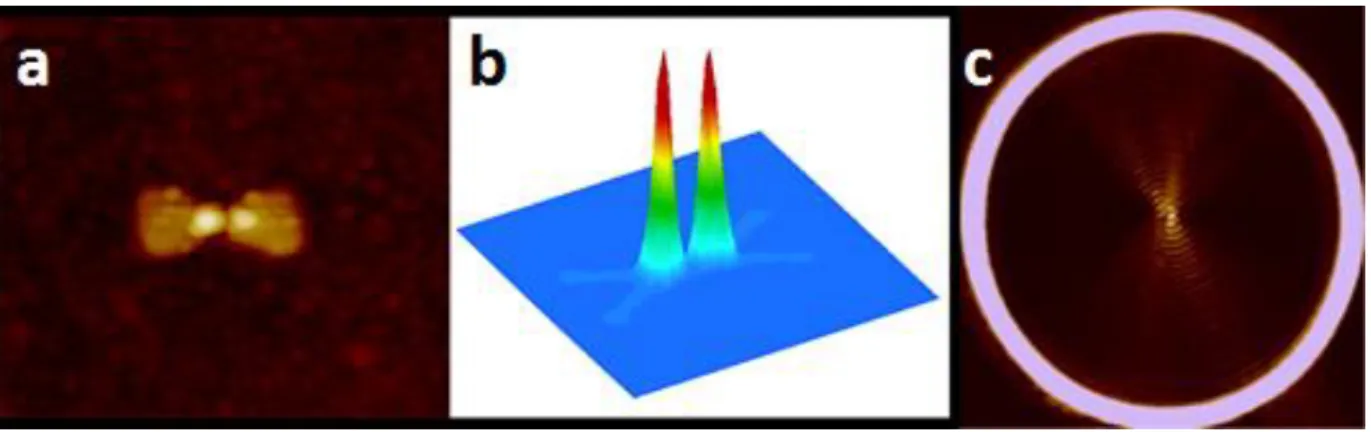
Infrared radiation refers to the region of the electromagnetic spectrum with wavelengths between approximately 700 nm (430 THz) and 1 mm (300 GHz). Inset shows images of the copper antenna layer (left) and the backplane with cut wires (right) with FR4 as the dielectric. In Figure 1.5a, researchers covered a bowtie antenna with photoresist and illuminated the antenna at a low intensity so that the photoresist was exposed proportionally to the intensity of the local electric field enhancement.
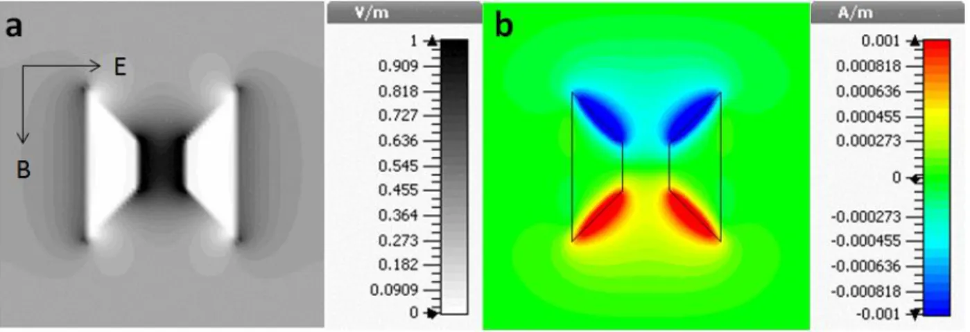
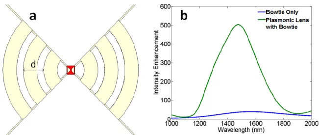
Both devices will have vanadium dioxide as the active material in the field concentration region between the two halves of the butterfly antennas. The dipole resonance results in a high field concentration between the two halves of the antenna, which is the optimal field profile to generate heat in the area where we will eventually place the VO2. We then tiled the butterfly in the two-dimensional plane of the surface and placed electrical leads along the outer edges of each antenna as shown in Figure 2.2a.
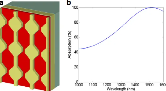
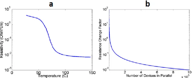
The resistance change factor (RCF) is given by 𝑅𝑓 = 𝑅𝑖(1 − 𝑅𝐶𝐹) where 𝑅𝑓 is the resistance of the array after switching and 𝑅𝑖 is the resistance of an unswitched array. For the plasmonic lens structure, we determined the distance between the rings using the lattice equation. For this structure, a small piece of VO2 was placed in the center of the bowtie antenna, instead of the continuous VO2 film used in the MPA geometry, and the reflective backplane was removed.
Vanadium dioxide is modeled as a small red square (500 nm on a side) in the center of the lens. To achieve a better understanding of the sensitivity of our devices, we will now consider the responsiveness, which is given by. A final area where our devices will outperform traditional bolometers is detection speed, which will be limited by VO2 transit time and thermal relaxation of the system.
Fabrication
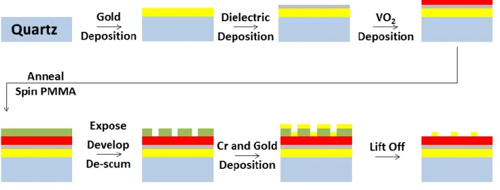
VO2 is annealed and coated in PMMA, which is exposed by electron beam lithography. After development and a defoaming step, the sample is coated in a layer of Cr and gold. The remaining PMMA and unwanted Cr/gold are removed by a lift-off procedure, leaving a functional device with a patterned antenna layer.
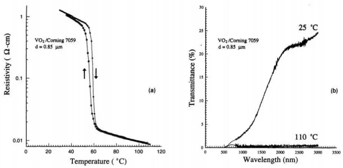
Conversion of the bulk VO2 films was confirmed and characterized by measuring the magnitude of transmitted light, or the spectrum of reflected light, for a white light source as the sample was heated from room temperature to 90 °C. Resistive switching was measured by varying temperature or bias on a resistive structure consisting of a 1 x 1 µm or 5 x 5 µm patch of VO2 deposited over gold electrodes on quartz or sapphire. The stoichiometry of the films was independently confirmed by the presence of characteristic RAMAN peaks at 192 and 222 cm-133.
The thickness of the VO2 films was confirmed with an atomic force microscope (AFM) after annealing, because the annealing step can cause changes in both the thickness and surface morphology of VO2 films. Samples were prepared for electron beam lithography (EBL) by spin coating with A-5 PMMA (5% in anisole) at 4000 rpm for 45 seconds, and then gentle baking in air at 180°C for two minutes. Samples were developed for 2 min in a 3:1 IPA:MIBK solution, which was allowed to thermally equilibrate with an ice-water bath for several minutes prior to development.
Samples were etched in a 120W oxygen plasma for 3 seconds to clean the exposed VO2 surfaces of any remaining developed PMMA. To confirm that the plasma clean did not damage the VO2, some bare VO2 samples were etched in an oxygen plasma for several minutes and then characterized as described above. Unexposed PMMA was removed by lifting for at least one hour in a PG remover bath heated to 70 °C.
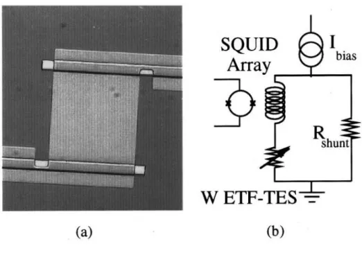
The gold thickness was determined by AFM and the device dimensions were determined by a combination of AFM and SEM. Devices were then mounted on a ceramic wireless chip carrier (LCC), in which all cables were shorted at all times when the device was not being tested, and electrically connected by wire bonding.
Measurement and Results
Figure 3.4 shows a schematic representation of the setup used for the optical characterization of the bowtie MPA structure. The resistance was determined analytically to correspond to a single pass of current from the interconnect pads, through the VO2, to the reflective backplane, rather than along the power rails and through the VO2 past the gap between the antennas, as designed. This failure of the dielectric film to wet the gold substrate effectively shorted the device at the interconnect pads, preventing us from electrically characterizing the MPA structures.
The growth of the dielectric layer is still in an island-forming regime, resulting in a discontinuous and ineffective dielectric barrier. After deposition of the alignment markers, the VO2 patches were defined by either a lift off method or plasma etching. As expected, the increased crystallinity of VO2 on sapphire substrates resulted in increased repeatability and the extent of switching as seen in
The EBL patterning of the antenna layer translated well to sapphire substrates, but when VO2 was etched onto sapphire a number of problems arose. When etching times were increased to remove any unwanted VO2, there was a large shelf (up to 1 µm) around each pattern element on which the VO2 was over-etched to a thickness of ~10 nm, regardless of the original thickness of the bulk thin film. This shelf can be seen in Figure 4.3, where the high crystallinity of the VO2 is clearly visible as a series of star-shaped patterns on the surface of the unetched material.
It was found that there are two etch stages for VO2 on sapphire, with the first ~10 nm above the lattice-matched and strained sapphire being etched more slowly than the rest of the film. While the switch to the lift method was necessary to allow accurate definition of the VO2 patches, it added a bigger problem by forcing us to glow VO2 internally. When we developed a method for realizing the structure of a plasmonic lens, we devoted ourselves to the electrical characterization of the device's operation.
The temperature of the devices was controlled locally by the magnitude of the applied voltage or across the sample using a resistance heater. Initial tests with high laser powers (1 W) resulted in a strong circuit, albeit with a clear locking of the resistance state. Since sensitivity is defined by both the response to a signal, which for resistance was a function of known and fixed material properties, and by the noise level of the device, we decided to characterize the noise level of our resistors.
Both effects together reduce the sensitivity of the device well below the theoretical sensitivity. Further matching between predicted and realized optical properties can be achieved by improved control over the structure dimensions.