IMPACT OF TEMPERATURE ON SINGLE-EVENT TRANSIENTS IN DEEP SUBMICROMETER BULK AND SILICON-ON-INSULATOR
DIGITAL CMOS TECHNOLOGIES
By
Matthew John Gadlage
Dissertation
Submitted to the Faculty of the Graduate School of Vanderbilt University
in partial fulfillment of the requirements for the degree of
DOCTOR OF PHILOSOPHY in
Electrical Engineering May, 2010 Nashville, Tennessee
Approved:
Professor Ronald D. Schrimpf Professor Bharat L. Bhuva
Professor Robert A. Reed Professor W. Timothy Holman
Professor Senta V. Greene
Copyright © 2010 by Matthew Gadlage All Rights Reserved
ACKNOWLEDGMENTS
I have so many people that I would like to thank for making this work possible, but first and foremost I would like to thank my family for their incredible support and encouragement. I would also like to give a special thanks to my little brother, Dr. Mark Gadlage, who was able to share this entire graduate school experience with me.
Special thanks also go to all the past and present students of the RER group for all their help in this effort, especially Dr. Balaji Narasimham for aiding in the SET measurement circuit design, Jon Ahlbin for help with testing and TCAD simulations, and Vishwa Ramachandran for his incredible work with the extreme heavy-ion temperature testing. I would also like to thank all of the professors from the RER group who are not on my committee for all of the helpful discussions over the years.
I would also like to thank Dr. Ronald Schrimpf and Dr. Bharat Bhuva for being great mentors throughout this whole process. Also, I’d like to thank the rest of my committee;
Dr. Robert Reed, Dr. Tim Holman, and Dr. Senta Greene for their help in finishing this dissertation.
I want to give a special acknowledge to some industry partners who helped make this work possible including Dr. Pascale Gouker at MIT Lincoln Laboratory for providing the SOI test circuits and beam time to test them and Robert Shuler of NASA Johnson Space Flight Center for help with the heavy-ion temperature testing.
A final thank you goes to NSWC Crane for their financial support of this effort and for providing me the opportunity to pursue this degree. I would especially like to thank Lydell Evans and Steven Clark of NSWC Crane for their encouragement and enthusiasm.
TABLE OF CONTENTS
Page
ACKNOWLEDGMENTS ... iii
LIST OF TABLES ... vi
LIST OF FIGURES ... vii
Chapter I. INTRODUCTION ...1
II. SINGLE-EVENT EFFECTS – BACKGROUND...4
CMOS Scaling...4
Space Radiation Environment ...6
Single Event Mechanisms ...8
Bulk and Silicon-on-Insulator Technologies...9
Digital Single Event Transients...11
Single Event Testing ...13
SET Measurements ...15
Narasimham Measurement Structure ...16
III. SINGLE EVENT TRANSIENT PULSE WIDTH MEASUREMENTS IN DEEP SUBMICROMETER BULK TECHNOLOGIES ...20
Introduction ...20
Pulse Broadening the 90-nm Test Structure...21
Pulse Broadening the 65-nm Test Structure...24
Impact of the N-well Contact on SET Widths ...27
Transistor-to-Transistor Spacing...30
Conclusions ...36
IV. SINGLE-EVENT TRANSIENTS IN A 180-NM FULLY-DEPLETED SOI TECHNOLOGY...38
Introduction ...38
180-nm FDSOI Test Chip Description...39
Heavy Ion Test Results ...40
Extracting SET Widths from the Floating Body Circuit...43
Mixed-Mode Simulations...46
Discussion ...50
Conclusions ...53
V. TEMPERATURE CHARACTERIZATION OF SINGLE-EVENT
TRANSIENTS...55
Introduction ...55
130-nm Bulk...56
90-nm Bulk...69
65-nm Bulk...74
180-nm Fully-Depleted SOI...77
Discussion ...80
Conclusions ...83
VI. EFFECT OF TEMPERATURE ON SET PULSE WIDTHS INDUCED IN NMOS AND PMOS DEVICES ...85
Test Structures...86
Single Event Test Results...87
Conclusions ...91
VII. CONCLUSIONS AND FUTURE RECOMMENDATIONS ...93
Key Results and Findings...93
Conclusions ...93
Future Recommendations...95
REFERENCES ...99
LIST OF TABLES
Table Page
1. Average and maximum 180-nm FDSOI SET pulse width values for xenon (LET=52.3 MeV-cm2/mg) at temperatures of 25˚ C, 50˚ C, and 100˚ C...77 2. Conductivity factors used for Fig. 7.1. ...96
LIST OF FIGURES
Figure Page
2.1. A plot from Intel [Chau-05] showing how the physical gate length of a transistor has continued to shrink over the past two decades. ...5 2.2. Flux of energetic particles in space as a function of linear energy transfer (LET) [Xaps-06] ...7 2.3. Illustration showing the different charge collection mechanisms during a single event [Baum-05] ...9 2.4. Cross-section of a bulk and SOI transistor ...10 2.5. Figure detailing how charge collected at a circuit node can create a transient signal that can propagate through a logic chain [Nara-08]...12 2.6. SETs arriving at the latching edge of a clock can be recorded as incorrect bits [Mavi-02] ...13 2.7. Cross-section versus frequency for several different operating voltages [Gadl-07].14 2.8. Illustration detailing how an SET with a width of two inverter delays propagates through an inverter chain [Nara-06] ...16 2.9. An illustration of the technique used in the autonomous SET measurement circuit to capture pulse widths [Nara-06] ...17 2.10.Diagram of the complete self-triggering autonomous SET test structure with reset [Nara-06] ...18 3.1 Maximum SET widths measured in 130-nm, 90-nm, and 65-nm test structures ...21 3.2 Schematic of the 1000-inverter chain target circuit in the 90-nm test structure. The laser strike location was at the center of each row...22 3.3 Laser results from the 90-nm SET test structure. Using the same laser energy to strike different locations in the inverter chain shows that as the SET propagates through it widens at a rate of nearly 1 ps/inverter ...23 3.4 SET measurements made on the 65-nm test structure at the microbeam facility...24 3.5 SET cross-section comparison for the 1000-inverter chain target circuit and the 10x100 inverter chain target circuit. ...25
3.6 Maximum generated SET pulse widths for the three test structures. ...26
3.7 Illustration of a parasitic bipolar transistor in a pMOS device [Olso-07] ...27
3.8 Simulation Results by Amusan et al. showing how the well contact size can affect SET pulse widths [Amus-07]. ...28
3.9 Illustration of the well contacting scheme used for each of the test structures...29
3.10 Maximum SET widths plotted as a function of n-well contact area percentage. ...29
3.11 Illustration of the layout of the same well inverter chain target circuit. ...31
3.12 Illustration of the layout of the separate well inverter chain target circuit. ...31
3.13 Average measured SET width versus LET for the separate well and same well test 65-nm test structures. ...32
3.14 Histogram of the measured SETs for the two 65-nm structures for an LET of 60 MeV-cm2/mg...33
3.15 SET error map of the separate well target circuit taken at the microbeam facility. .34 3.16 SET error map of the same well target circuit taken at the microbeam facility ...34
3.17 Examples of some of the multiple SET events measured during heavy ion testing of the separate well circuit. ...35
3.18 Comparison of the multiple SET cross-section to the single SET cross-section for the separate well target circuit. ...36
4.1 Average measured SET widths for various strike locations in the inverter chain target circuit for the floating-body FDSOI test structure...39
4.2 SET pulse width distributions for argon (LET = 14 MeV-cm2/mg, Fluence = 1x10⁹ particles/cm2). Note that not only are the pulse widths shorter for the circuit with source-body contacts, the total the number of counts is also significantly less. ...41
4.3 SET pulse width distributions for krypton (LET = 40 MeV-cm2/mg, Fluence = 7x10⁸ particles/cm2). ...41
4.4 SET pulse width distributions for xenon (LET = 69 MeV-cm2/mg, Fluence = 4x10⁸ particles/cm2). ...42
4.5 SET pulse width distributions for bismuth (LET = 100 MeV-cm2/mg, Fluence = 2x10⁸ particles/cm2). ...42
4.6 Average SET pulse widths experimentally measured for the two target circuits. The error bars represent one standard deviation from the average. ...43
4.7 Plots of a possible original distribution of SETs without pulse broadening, the distribution obtained by convolution of the broadening-caused effects, and the
actual measured SET events. ...45
4.8 Illustration of the mixed-mode model used for the simulations. The second nMOSFET in a four inverter chain was modeled in 3D TCAD, and the remaining inverters were modeled in SPICE. ...46
4.9 Comparison of measured and simulated I-V curves for a device in this technology47 4.10 Simulated SET pulse widths at the struck node for an LET of 40 MeV-cm2/mg for the non-body contacted device and the body contacted device. The ion strike location in this simulation was the center of the gate. ...48
4.11 Simulated SET pulse widths for the floating-body device showing the pulse width dependence on the ion strike location. As the strike location moves away from the center of the gate, the SET pulses become smaller. An ion strike at the center of the drain creates no SET. ...49
4.12 Simulated SET pulse width distributions for strikes on the nMOS device for the ions used in testing...50
4.13 Simulated SET pulse width for a strike on the pMOS device with an LET of 100 MeV-cm2/mg...51
4.14 Comparison of bulk and SOI SET cross-sections...53
5.1 130-nm stage delay as a function of temperature. ...56
5.2 Illustration and photograph of the cryogenic test system used in this work...57
5.3 SET cross-section as a function of temperature...58
5.4 Measured SET pulse width histogram at room temperature. The histograms (in units of latch delays) were similar for all temperatures...59
5.5 Measured SET pulse width histogram (with error bars) at room temperature. ...60
5.6 Average SET pulse width in units of latch delays. ...62
5.7 Average SET pulse width for the cold temperature testing. ...63
5.8 Photograph of the test setup for all of the elevated temperature testing performed in this work...64
5.9 Average SET pulse width for the elevated temperature testing of the 130-nm test circuits...65 5.10 A 130-nm TCAD model used to study the effect of temperature on SET pulse
widths using a mixed mode simulation. For the 130-nm bulk device, either the off state pMOS or nMOS device was modeled in 3D TCAD ...66 5.11 Results of the 130-nm mixed-mode simulation of the pMOS device showing SET pulses on the struck node for five temperatures...67 5.12 Results of the 130-nm mixed-mode simulation of the nMOS device showing SET pulses on the struck node. ...68 5.13 Results of the 130-nm mixed mode simulation showing the drain current on the struck node of the pMOS device for five temperatures. ...68 5.14 Results of the 130-nm mixed mode simulation showing the current on the struck node of the p-diode for five temperatures...69 5.15 Bipolar enhancement factor plotted as a function of temperature ...71 5.16 90-nm bulk SET pulse width distribution for xenon (LET=52 MeV-cm2/mg) at temperatures of 25˚ C, 50˚ C, and 100˚ C. At 100o C, some of the SETs were longer than the measurement limit of the test circuit...71 5.17 90-nm bulk SET pulse width distribution for xenon at an incident angle of 50o
(Effective LET=81 MeV-cm2/mg) at temperatures of 25˚ C, 50˚ C, and 100˚ C ...73 5.18 Plots of a possible original distribution at 25o C of SETs without pulse broadening, the distribution obtained by convolution of the broadening-caused effects, and the actual measured SET events ...73 5.19 Plots of a possible original distribution of SETs without pulse broadening for 25o C, 50o C, and 100o C. ...75 5.20 Measured SET pulse width distribution for the same well inverter chain circuit.
Note that as the temperature increases the distribution shifts to the longer SET widths...76 5.21 Measured SET pulse width distribution for the separate well inverter chain circuit.76 5.22 Average SET width measurements as a function of temperature for the separate
well and same well 1000-inverter chain target circuits. ...78 5.23 Results of the 180-nm FDSOI mixed mode simulation for the nMOS device showing SET pulses on the struck node for 25˚ C, 50˚ C, and 100˚ C. ...79 5.24 Results of the 180-nm FDSOI mixed mode simulation for the pMOS device showing SET pulses on the struck node ...79 5.25 Laser induced SET pulse width in a FDSOI process as a function of temperature ..80 5.26 Simulated drain current as a function of temperature for the 65-nm nMOS and
pMOS devices used in the inverter chain target circuit ...83 6.1 Schematic of two of the blocks of “N-hit” target circuit. The target circuit used in this work consisted of four linear chains of 100 of these combinational logic blocks
“OR”-ed together to form a single output...86 6.2 Schematic of two of the blocks of “P-hit” target circuit. The target circuit used in this work consisted of four linear chains of 100 of these combinational logic blocks
“OR”-ed together to form a single output...86 6.3 Layout of two of the blocks of “N-hit” target circuit. The spacing between the two inverters needs to be large enough to ensure that an ion can not induce an SET on both at the same time ...87 6.4 SET cross section for the different 65-nm test structures. Note that the threshold LET for the “P-hit” and “N-hit” circuits are much larger than for the inverter chain circuits...88 6.5 Average SET width as a function of temperature for the “N-hit” and “P-hit”
circuits...89 6.6 Measured SET pulse width distribution for the “P-hit” circuit. Note that as the temperature increases the distribution clearly shifts to the longer SET widths...90 6.7 Measured SET pulse width distribution for the “N-hit” circuit. Due primarily to the small number of SETs measured, changes in the SET width distribution are difficult to observe ...91 7.1 Maximum SET width plotted as a function of the conductivity of the n-well ...97
CHAPTER I
INTRODUCTION
For over thirty years, ionizing particles have been affecting semiconductor reliability.
In the 1970’s, the first single-event effects due to cosmic rays [Bind-75, Pick-79] and alpha particles [May-78, May-79] were reported. With the rapid advancement in semiconductor technology since then, new single-event phenomena have emerged. In the late 1990's, advanced electronics became fast enough that a new effect in digital circuits, known as single-event transients (SETs) appeared. During the 2000’s, researchers predicted that these SETs would become the dominant semiconductor electronic reliability issue [Shiv-02]. While some researchers predicted that the SET problem would become worse with each technology node [John-00, Gadl-04, Dodd-04, Nara-07], many seemingly conflicting results were reported. As one example, Baze et al. [Baze-06]
measured the maximum time duration of these SETs in a 130-nm technology to be around 300 ps, while data published by Benedetto et al. [Bene-06] showed that SETs could be upwards of 2 ns in a nearly identical technology.
With the large amount of research on SETs, one aspect that has been mostly ignored has been the effect of temperature on the time duration of these transients. The temperature ranges over which some space missions need to operate can be extreme.
Thus, the role of temperature for all radiation effects is of vital importance for space systems. For example, on the moon the temperature can range from -230°C to +120°C.
So while it is known that SETs can be a reliability issue for space electronics, the impact
of temperature on these SETs remains largely unknown. Determining the effect of temperature on SETs is the key aspect of this dissertation. However, to understand fully how temperature will impact SETs, a complete understanding of SETs at room temperature is needed. As illustrated by the example of the Baze and Benedetto research, this alone is no easy task and is an ongoing active research area. In this dissertation, data from over a dozen experiments on ten SET test structures fabricated in a myriad of semiconductor technologies will be presented. The data from these test structures give valuable insight into how the SET problem is changing with each new technology. With the understanding gained from these data, some of the questions of why different researchers have reported seemingly conflicting results are answered. Finally with the answer to some of the questions, for the first time, how temperature affects the time duration of SETs is explored.
This dissertation begins with an introduction to semiconductor technology and the space radiation environment. SETs are defined in detail and their relationship to semiconductor reliability is explained. In the final section of Chapter II, an SET measurement circuit that is used throughout the dissertation is introduced. In Chapter III, factors affecting SETs at room temperature in “bulk” semiconductor technologies are discussed. An in-depth look at why different test circuits can give conflicting results is provided. The dissertation then looks at SETs in a different semiconductor process known as silicon-on-insulator (SOI) in Chapter IV. The data presented in Chapters III and IV set the foundation for the "heart" of the dissertation in Chapter V. In Chapter V, data on SETs in four different technologies taken over wide temperature ranges are presented.
The mechanisms responsible for SETs changing with temperature are also discussed. In
Chapter VI, lessons learned from the mechanisms impacting SETs over temperature lead to the development of unique test structures and a set of data that experimentally confirm the key hypothesis presented in Chapter V. In the final chapter, a short data analysis is presented that helps define future directions for exploring the SET problem.
CHAPTER II
SINGLE-EVENT EFFECTS - BACKGROUND
Ionizing radiation can cause a considerable number of negative effects for space- based electronics. Different types of radiation effects include total-dose [Lera-99, Schw- 02, Barn-05, Oldh-03, Alex-03, Glov-80], displacement-damage [Srou-88, Summ-92], and single-event effects [Pete-83, Pick-83, McNu-90, Sext-92, Mass-93]. In this dissertation, only single-event effects will be discussed. Single events can be classified into several types [Dodd-03] including: single-event upsets (SEUs), single-event latchup (SEL), single-event burnout (SEB), single-event gate rupture (SEGR), and single-event transients (SETs). Single-event transients can be broken down further into analog or digital SETs. This dissertation focuses primarily on digital single-event transients. A digital SET is nothing more than a glitch induced by a radiation event in a digital circuit.
The mechanisms and conditions under which a digital SET can be a problem are discussed later in this chapter.
The rest of this chapter consists of: the scaling of digital CMOS technologies, the space radiation environment, single-event transient mechanisms, the difference between bulk and SOI (silicon-on-insulator) technologies, and single-event testing. The chapter concludes with a description of an SET measurement circuit that will be used throughout this dissertation.
CMOS Scaling
In the late 1950’s, the first integrated circuit (IC) was developed by Jack Kilby of
Fig. 2.1: A plot from Intel [Chau-05] showing how the physical gate length of a transistor has continued to shrink over the past two decades.
Texas Instruments [Kilb-63]. Since then the number of transistors on an integrated circuit has been growing exponentially. The rapid growth in IC technology has led to significant improvement in both computer and mobile electronic functionality. A concept developed by Gordon Moore (the founder of Intel), known as Moore’s law, has been used to describe the rapid advancement in the semiconductor industry [Moor-65]. One variation of Moore’s law states that the number of transistors that can be placed on an IC doubles every two years. (Another interpretation of Moore’s law states that processing power, speed, and number of DRAM cells double every 18 months to two years.) One side effect of the improvement in semiconductor technology has been that electronic devices have become more susceptible to certain radiation effects. In particular, the closer spacing of transistors, smaller nodal capacitances, and lower operating voltages associated with CMOS scaling have all led to enhanced susceptibility to single event
effects.
With every new semiconductor technology, a dimension known as the feature size is used to characterize that technology. The feature size is a measure of the smallest element possible on an IC fabricated in that technology. In advanced ICs, feature sizes are usually measured in nanometers. Traditionally, the smallest feature size was equal to the width of the gate (i.e., the distance from the drain to the source in a MOS transistor), however, in sub 100-nm technologies the effective width of the gate may actually be smaller than the feature size. In this dissertation, single-event transients will be discussed in technologies with feature sizes ranging from 180 nm down to 65 nm.
Space Radiation Environment
Advanced electronic devices often have to operate in harsh environments. Perhaps the harshest of these environments is the space environment. Outside the earth’s atmosphere, spacecraft electronics face a constant bombardment of highly energetic particles. These energetic particles can come from one of three sources [Xaps-06]. The first includes particles trapped in the Earth’s magnetic field in what are known as the Van Allen Belts. The second includes all radiation from the sun (typically emitted in bursts known as solar events). The final source of energetic particles is galactic cosmic rays that originate outside our solar system.
When one of these energetic particles passes through a material, it loses energy through interactions with the material. The energy loss is due primarily to the interactions of the particle with bound electrons in the material. These interactions cause the direct ionization of the material and the formation of a dense track of electron-hole
Fig. 2.2: Flux of energetic particles in space as a function of linear energy transfer (LET) pairs. A commonly used term for the energy deposited by an ion as it passes through a material is linear energy transfer (LET). The LET is a measure of the energy deposited per unit length as a particle travels through a material. LET values are usually given in units of MeV-cm2/mg, which is the energy deposited per unit length divided by the density of the target material. In space, the lower the LET of the energetic particle, the higher the probability it has of occurring. As seen in Fig. 2.2, a particle with an LET of 1 MeV-cm2/mg is approximately 10 orders of magnitude more likely to occur than a particle with an LET of 100 MeV-cm2/mg.
Highly energetic particles can also generate electron-hole pairs through a process known as indirect ionization (as opposed to the direct ionization process discussed in the previous paragraph). Indirect ionization occurs when an energetic particle causes a nuclear reaction with a material in an IC. The byproducts of the reaction create the
ionizing particles that directly create the electron-hole pairs. It is through this indirect ionization process that neutrons (and high-energy protons) are also able to cause single- event effects.
Single Event Mechanisms
By knowing the LET of the heavy ion generating charge through direct ionization, one can calculate the number of electron-hole pairs created if the ion strikes a silicon wafer. This knowledge goes a long way in helping to quantify single-event effects. In silicon, about 3.6 eV is needed to create one electron-hole pair. Knowing that the density of silicon is 2.42 g/cm3, one can find the number of electron hole pairs created per ion track length (L) by using the following equation [Mavi-02]:
Q (fC) = 10.8 x L (µm) x LET (MeV-cm2/mg)
Thus an ion with an LET of 1 MeV-cm2/mg will leave approximately 10.8 fC along each micrometer of its track.
For generated charge to cause a single event, the charge has to be collected at a circuit node. Three primary mechanisms affect the amount of charge collected in an electronic device: drift, diffusion, and recombination. Drift describes the movement of charge (electrons and holes) in the presence of an electric field. Diffusion is the movement of charge due to a concentration gradient. Finally, recombination occurs when electrons and holes annihilate one another.
Charge is collected primarily only when an ionizing particle passes through a depletion region. Since depletion regions are largest around reverse-biased junctions, the sensitive region of a CMOS device is typically limited to the reversed-bias drain/well (or drain/substrate) junctions. The drift component of charge collection consists primarily of the charge collected promptly as the ion passes through the depletion layer. However, the ion track can cause a potential contour deformation that leads to the depletion layer extending deeper into the device in the direction of the ion track. This extension of the depletion layer is known as “funneling” and it results in the collection of additional charge [Hsie-81].
Bulk and SOI Technologies
In this dissertation, single-event transients in two types of semiconductor technology will be discussed: bulk and silicon-on-insulator (SOI). As the name “silicon-on- insulator” suggests, an SOI technology consists of a silicon layer on top of an insulating layer [Coli-01]. The insulating layer is typically silicon dioxide (SiO2) (but can also be a
Fig. 2.3: Illustration showing the different charge collection mechanisms during a single event [Baum-05]
different insulator material such as sapphire). The transistors are placed in the silicon layer above the insulating layer. The addition of the insulating layer reduces parasitic capacitances and eliminates any latchup path. The insulating layer also limits the amount of charge that can be collected from a single event [Muss-01]. As illustrated in Fig. 2.4, the amount of charge that can be collected in an SOI technology is limited to the thickness of the silicon layer, whereas in a bulk technology charge generated up to several micrometers below the transistor can still be collected. Due to the reduced amount of collected charge in SOI processes (when compared to bulk), SOI has become a promising technology for use in environments where single event effects are of concern.
An SOI technology can either be partially-depleted or fully-depleted. The simple difference between the two is that in a fully-depleted SOI (FDSOI) technology, the depletion region extends all the way to the buried oxide (BOX) of the device, while in a partially depleted SOI (PDSOI) technology the depletion layer does not extend all the
Fig. 2.4: Cross-section of a bulk and SOI transistor
way to the BOX. Because of this, the thickness of the silicon layer in a FDSOI technology is typically thinner than the silicon layer of a PDSOI technology. Due to the thinner silicon layer and thus smaller volume available to collect charge, a FDSOI technology is often less susceptible to radiation effects than a PDSOI technology. One of the goals of this dissertation is to explore differences in SETs between bulk and FDSOI technologies.
Digital Single Event Transients
In a traditional digital circuit, two types of logic circuits can be defined:
combinational logic and storage logic. Some examples of storage logic circuits include latches and flip-flops. In this type of circuit the error rate due to single events is almost independent of the clock frequency of the circuit. The latch or flip-flop's state can be flipped by an ionizing particle creating charge on a node regardless of the state of the clock signal at its input. Some examples of combinational logic circuits include NAND gates, XOR gates, and inverters. Single-event transients induced in the combinational logic circuits between storage cells can arrive at the input of the storage cell on the latching edge of the clock and be clocked in as erroneous data. Thus errors due to the combinational logic being hit by an ionizing particle depend on the clock frequency [Kaul-91, Reed-96, Buch-97]. The faster the clock, the more latching clock edges there are available to capture a transient signal.
The probability for a transient pulse to get latched as an incorrect data bit depends on its width [Baze-97, Mass-00]. Transient pulse propagation also depends on the state of the other combinational logic in its path. For example, if a transient pulse arrives at one
input of a NAND gate, but the other input of the NAND is at logic zero, then the transient pulse will not propagate through. Assuming the transient pulse propagates through the logic, the wider the pulse width, the greater the probability it has of arriving on the latching edge of the clock. If the transient pulse becomes longer than the time period of the clock, then every induced transient pulse will be latched. Fig. 2.6 illustrates how the width of an SET determines the probability of whether or not the SET will be latched. In this figure, the data will latch on the clock's falling edge. From the figure, one can see
Fig. 2.5: Figure detailing how charge collected at a circuit node can create a transient signal that can propagate through a logic chain [Nara-08].
how a wider SET width will lead to a greater probability of the SET arriving on the latching edge of a clock signal.
The impact of clock frequency and SET pulse widths on error rates is shown in Fig.
2.7. The data in the figure come from a test structure in which only the only errors came from SETs that arrived at the latching edge of a clock [Gadl-07]. In this figure, one can see that as the clock frequency is increased, the cross-section also increases. (The cross- section in this figure is the number of single events observed divided by the total fluence of particles.) Also in this figure, one can see that the lower operating voltages also increase the cross section. (The higher cross-section at the lower operating voltages can be attributed to an increase in SET width with decreasing voltage.)
Fig. 2.6: SETs arriving at the latching edge of a clock can be recorded as incorrect bits [Mavi- 02].
Single-Event Testing
To help quantify the effects of ionizing radiation in space on electronics, several facilities have been developed in the United States to perform single event testing [Buch- 96, Duze-96]. In this work, four of these facilities will be discussed: (1) an 88’ cyclotron at Lawrence Berkeley National Labs, (2) the Texas A&M University cyclotron, (3) a
“microbeam” facility at Sandia National Labs, and (4) focused laser-based systems at the U.S. Naval Research Lab (NRL). (Note: these are not the only facilities available for single-event testing; a more complete list can be found in [Buch-96].) The Berkeley and Texas A&M facilities are both what are known as “broadbeam” facilities. Both of these cyclotrons are capable of accelerating ions of numerous atoms to energies ranging from 10 to 40 MeV per atomic mass unit (amu). To perform testing at these broadbeam facilities, electronic components are placed directly in the ion beam generated by the cyclotron. Single-event effects are monitored while the electronics-under-test are
Fig. 2.7: Cross-section versus frequency for several different operating voltages [Gadl- 07]
operated. Typically at a heavy ion facility, one will record the data in terms of a “cross- section”. A single-event cross-section from a “broadbeam” facility is usually defined as the number of errors (or single events) measured divided by the total fluence of particles.
Sandia National Laboratories’ Ion Beams Materials Research Lab operates a tandem Van de Graaff accelerator which has several ion species. The Sandia “microbeam”
facility is able to focus the ions to an area as small as a square micrometer. The focused lasers at NRL shrink a laser spot down to approximately one square micrometer [McMo- 02]. Laser-induced carriers can be injected through the backside of a silicon die using a Two-Photon Absorption (TPA) technique or through the front of the device using a pulsed infrared laser [McMo-02]. An advantage of the TPA approach is its ability to interrogate SEE phenomena and circuit vulnerability through the wafer using backside irradiation, thereby eliminating interference from the metallization layer stack.
The key feature of using either the Sandia microbeam facility or the NRL laser based system is that one knows exactly where the single event occurs. The micrometer-sized laser spot or focused-ion beam can be maneuvered to strike various known locations in an electronic circuit. In a “broadbeam” such as at Berkeley or Texas A&M, the ion may strike any location of the device.
SET Measurements
As discussed previously, knowledge of SET pulse widths is crucial to determining the probability of an SET creating an error. Because of this, numerous researchers have attempted to experimentally measure digital SET pulse widths in deep submicron bulk technologies. Measuring SET pulse widths has been accomplished using several
techniques. SET pulses can be directly measured using high speed oscilloscopes [Ferl- 06, Ferl-06-1, Pell-08]. However, such direct off-chip measurements are extremely difficult to perform because loading (and line) capacitances can significantly alter the SET shape. As a result, several on-chip SET measurements have been developed. Test structures developed by Baze et al. [Baze-06] and Eaton et al. [Eato-04] use a delay- based technique. The idea behind both techniques is that all transients shorter than a known delay will be filtered. Thus, once the delay becomes longer than the SET width, no SETs are measured. This provides an indirect way of measuring SET widths. In 2006, Narasimham et al. developed a technique that is able to directly measure digital SET pulses on-chip [Nara-06]. The Narasimham SET measurement technique will be used throughout this dissertation, and a complete description is given in this chapter.
Autonomous Pulse Capture and Measurement Structure
The autonomous SET measurement circuit characterizes SET pulse widths in units of inverter (or latch) delays. The idea behind the circuit is that as a transient signal propagates through a combinational logic chain, at any given time, the number of logic
Fig. 2.8: Illustration detailing how an SET with a width of two inverters delays propagates through an inverter chain [Nara-06]
gates affected by the transient depends on its width. This is illustrated in Fig. 2.8. In this figure, an SET with a width of two inverter delays is shown. The autonomous SET measurement circuit effectively measures the number of inverters affected by a transient.
If one knows the inverter delay, one can then determine the SET width that will be accurate to within ± one-half of the inverter delay.
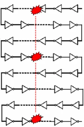
To capture the number of inverters affected by an SET, a latch can be connected to the output of each inverter as shown in Fig. 2.9. As the SET travels through the inverter chain, the data in the latch corresponding to each inverter will change. However, once the SET propagates through, the inverter output, latch data will change back to their original states. One of the keys to making the SET measurement circuit work is the ability to capture and hold an SET.
To capture and hold a generated SET, the inverter stages in the measurement circuit can be created with pass and hold gates as shown in Fig. 2.10. The circuit shown in Fig 2.10 is self-triggering. When an SET generated in the target circuit arrives at the first stage, it continues to propagate through to the remaining stages and the delay. However,
Fig. 2.9: An illustration of the technique used in the autonomous SET measurement circuit to capture pulse widths [Nara-06]
once the SET propagates through the delay, the S/R latch will change the value of the pass and hold signals. Once the pass and hold signals are set, the SET is essentially frozen in each stage. The output of each stage in Fig. 2.10 is connected to a latch (as shown in Fig. 2.10). The data stored in these latches represent the value of the SET width in units of stage delay. The outputs of these latches are connected to a parallel-in-serial- out shift register that enables one to get the SET pulse width data off the chip.
To determine the delay of each stage in the measurement circuit, a ring oscillator is created using the same latches as used in the measurement circuit. By determining the frequency of the ring oscillator one can determine the individual stage delay.
The target circuit used to “collect” SETs can be almost any combinational logic chain. For the results to be presented in this dissertation, a linear chain of 100 inverters was used as the target circuit in a 130-nm bulk technology, a chain of 1000 inverters was used for a 90-nm bulk technology, a chain of 200 inverters was used for a 180-nm fully-
Fig. 2.10: Diagram of the complete self-triggering autonomous SET test structure with reset [Nara-06]
depleted SOI technology, and a myriad of target circuits was used for a bulk 65-nm technology.
One minor issue with the autonomous SET measurement circuit is that it is unable to measure transients accurately that are shorter than a few latch stages. This issue has been reported in nearly every test structure that has utilized the autonomous SET measurement circuit [Nara-07, Nara-08, Gouk-08, Maki-09]. Narasimham attributed it to attenuation in the pulse capture latches and showed that for SETs greater than approximately three or four latch stages no attenuation occurred and the SET was measured correctly. The impact of this on the results presented in this dissertation is that if there are SETs generated smaller than three latch stages during testing, the measurement circuit will be unable to record them accurately.
CHAPTER III
SINGLE EVENT TRANSIENT PULSE WIDTH MEASUREMENTS IN DEEP SUBMICROMETER BULK TECHNOLOGIES
Introduction
As discussed in the previous chapter, knowledge of SET pulse widths is crucial to determining the probability of an SET creating an error. Because of this, a large amount of research has been performed measuring digital SET pulse widths in deep submicron bulk CMOS technologies. In this chapter, an overview of SET measurements and mechanisms that can affect those measurements in bulk technologies is given. In addition to giving a short review of previous measurements, SET measurement data will be presented from test structures fabricated in a bulk 65-nm technology. The data from these test structures are some of the first SET measurements ever performed in a 65-nm technology. Possible explanations for the differences in measured pulse widths between the technology nodes will be given. The data and analysis presented in this chapter will help set the foundation for the work dealing with SET width measurements over temperature that will be presented in Chapter V.
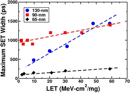
One item of key interest to the radiation effects community is knowledge of how SET pulse widths scale with technology. Since new technologies are only available approximately every two years, determining any trends with SET pulse widths has been a slow process. The maximum measured SET widths in several bulk technology nodes (all measured using the autonomous SET measurement circuit) are shown in Fig. 3.1. For each technology, the SETs were generated in a target circuit that consisted of a linear
Fig. 3.1: Maximum SET widths measured in the 130-nm, 90-nm, and 65-nm test structures
chain of inverters. In this figure, one can see that significant differences in the maximum SET width between the technology nodes exist. However, no trend or even consistent results between the technology nodes is apparent.
Pulse Broadening in the 90-nm Test Structure
Perhaps the most glaring difference between the measurements shown in Fig. 3.1 is the long SET widths measured at small LET values in the 90-nm technology node. The long SETs measured at the small LET values are particularly troublesome since the smaller the LET value the higher the probability of seeing an event in space. A more in- depth look at the 90-nm results reveals the primary reason for the large SET widths at the small LET values.
In the 130-nm circuit, the target circuit in which SETs are generated was a chain of 100 inverters. However, in the 90-nm circuit, the target was a chain of 1000 inverters.
Recent work by Ferlet-Cavrois et al. [Ferl-07] and Massengill & Tuinenga [Mass-08]
shows that transient signals can widen as they propagate through a combinational logic chain. A detailed description of the mechanisms behind this broadening effect is given by Massengill [Mass-08]. Obviously any broadening in the SET target circuit affects the SET measured by the measurement circuit.
To determine if the long SETs in the 90-nm circuit are due to pulse broadening, testing was performed using the two-photon focused laser at the Naval Research Lab [McMo-02]. The inverter chain in the 90-nm circuit consists of eight rows of 125
Fig. 3.2: Schematic of the 1000-inverter chain target circuit in the 90-nm test structure.
The laser strike location was at the center of each row.
inverters. Using the same laser energy, SETs were measured for different strike locations in the center of each row in the inverter chain. The results are shown in Fig. 3.3. A fairly significant broadening effect is observed. The broadening rate was almost 1 ps/inverter.
These results suggest that the large SET pulse widths observed at the small LETs for the 90-nm SET data are due to the layout of the target circuit.
The 130-nm test structure was also tested with the two-photon laser to look for pulse broadening. No pulse broadening was observed. If the broadening rate in the 130-nm circuit was the same as the 90-nm circuit (a reasonable assumption), the most any SET would be broadened in the 100-inverter chain would be 100 ps. 100 ps is on the order of the resolution of the measurement circuit for the 130-nm test structure.
Fig. 3.3: Laser results from the 90-nm SET test structure. Using the same laser energy to strike different locations in the inverter chain shows that as the SET propagates through it
widens at a rate of nearly 1 ps/inverter.
Pulse Broadening in the 65-nm Test Structure
For the 65-nm SET pulse width measurements shown in Fig. 3.1, the target circuit also consisted of a linear chain of 1000-inverters (similar to the 90-nm test structures).
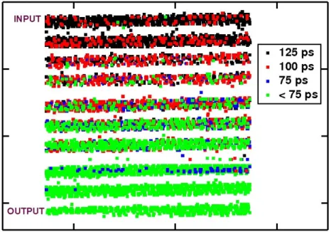
To explore the impact of pulse broadening on the 65-nm SET measurements, an experiment was performed at the Sandia Microbeam Facility using 36 MeV oxygen ions with an LET of 5.4 MeV-cm2/mg. The results of this experiment are shown in Fig. 3.4.
In this plot, each point represents a location at which an SET was measured. The 1000 inverter chain target circuit was designed with 10 rows of 100 inverters. The first row of inverters is at the top of the figure and the inverter chain snakes around to the bottom row before it enters the measurement circuit. This plot clearly shows that SETs generated away from the measurement circuit are broadening as they propagate through the logic chain. Near the input the average measured SET is approximately 125 ps, and about halfway through the inverter chain the pulses become shorter than 75 ps. From these
Fig. 3.4: SET measurements made on the 65-nm test structure at the microbeam facility
data, one can conclude that the broadening rate in this test structure is about 0.1 ps per inverter. This broadening rate is almost an order of magnitude less than that in the 90-nm test structure. The significance of this is that these results show that pulse broadening is not necessarily getting worse with technology scaling. The amount of pulse broadening depends on the circuit and layout design (not primarily the technology the circuit was designed in).
Not only can pulse broadening affect SET measurements, broadening can also impact the number of SETs measured. For example, in the 65-nm test structure an additional target circuit was designed with ten chains of 100 inverters “OR”-ed together to form a single output. Therefore, the average pulse broadening in this type of circuit should be about an order of magnitude less than in the linear 1000 inverter target chain circuit. In Fig. 3.5, the cross section to create an SET greater than 75 ps is plotted for the two different target circuits. The cross section is much smaller for the “OR”-ed circuit than
Fig. 3.5: SET cross-section comparison for the 1000-inverter chain target circuit and the
for the 1000 inverter chain circuit even though the total sensitive area is approximately the same. The reason for this is that many of the smaller SETs generated in the 1000 inverter chain are able to broaden to a width greater than 75 ps whereas in the “OR”-ed circuit they are not.
With the broadening in the measurement circuits determined, one can now take a look at the generated SET widths. The generated pulse widths are the pulse widths that would be measured if there were no pulse broadening in the test structure. The generated SET widths are plotted in Fig. 3.6. By assuming that the maximum SETs measured in the 90- nm circuit were SETs that were generated near the input to the target circuit and had propagated through nearly 1000 inverters before they were measured, one can assume that by subtracting 1000 ps from the maximum SETs in Fig. 3.1 the generated SET width can be found. A similar analysis can be performed on the 65-nm results. The maximum generated SET width, as shown in Fig. 3.6, suggest that the pulse widths may actually be
Fig. 3.6: Maximum generated SET pulse widths for the three test structures.
decreasing with technology node. However, in the next section, results will be presented that will show that this may not necessarily be the case.
Impact of the N-Well Contact on SET Widths
While the results presented in the previous section suggest that SET pulse widths will shrink with technology node, an observation of the mechanisms affecting charge generation and collection can give more insight into what to expect as feature size shrink.
One of the predominant mechanisms causing long SET pulse widths in deep submicron bulk technologies is parasitic bipolar amplification. In any MOS structure, a parasitic bipolar transistor exists. An illustration of a parasitic PNP bipolar transistor in a PMOS device is shown in Fig. 3.7. When an energetic particle (heavy ion) strikes such a device, this bipolar transistor can turn on and lead to an enhancement in the charge collected.
This increase in collected charge leads to an increase in SET width. Due to parasitic bipolar amplification, larger SET pulse widths are observed in pMOS devices than in nMOS devices. Parasitic bipolar amplification is more pronounced for a pMOS device in
Fig. 3.7: Illustration of a parasitic bipolar transistor in a pMOS device [Olso-07]
an n-well with a p-substrate for a bulk, twin-well CMOS process like the ones that are studied in this work.
Amusan et al. [Amus-07] showed that the parasitic bipolar effect and the SET pulse width depend significantly on the well contact size and spacing. Amusan’s results are shown in Fig. 3.8. As can be seen, SET pulse widths can be altered significantly by adjusting the well contact size. Amusan’s simulations show that the maximum SET width can vary by up to 1 ns for the same technology just due to differences in the n-well contact size. These results are important because they suggest that SET measurements can depend more on the layout of the transistors than the technology node (or the minimum feature size at a technology node).
Fig. 3.8: Simulation Results by Amusan et al. showing how the well contact size can affect SET pulse widths [Amus-07].
The results of Amusan et al. suggest that perhaps the smaller SET widths with the shrinking technology nodes may have little to do with the technology node itself but rather may be a function of how the n-well is contacted in the test structure. To further look into this, the well contact area for each of the test structures was measured and normalized to the total N-well area. In Fig. 3.9, an image of the well-contacting scheme for each test structure is shown. For each newer technology, the n-well was better
Fig. 3.9: Illustration of the well contacting scheme used for each of the test structures.
Fig. 3.10: Maximum SET widths plotted as a function of n-well contact area percentage.
contacted as seen by the ratio of the well-contact area to the total well area. In fact, if we plot the maximum SET width versus the contact area percentage, a plot (shown in Fig.
3.10) with a remarkable similarity to the one presented by Amusan et al. in Fig. 3.8 is found. The point of this analysis is to show that the smaller pulse widths measured with the newer technologies may not be related to the technology but rather may simply be a function of how the n-well is contacted. This well-contacting issue and its impact on the parasitic bipolar action will be discussed in the final chapter.
Transistor-to-Transistor Spacing
As feature sizes have scaled and the spacing between transistors has shrunk, a new mechanism has started to affect SET pulse widths. A mechanism known as “pulse quenching” [Ahlb-09] can occur when more than one device is able to collect charge.
The end result of this mechanism is that the resulting pulse width ends up being shorter when two electrically-related transistors collect charge than when only a single transistor collects charge. To explore this mechanism at the 65-nm technology node, two test circuits were developed. In the first circuit, an inverter chain was designed with each inverter spaced 0.75 µm apart and with each pMOS transistor placed in the same n-well.
The second circuit consisted of a schematically-identical inverter chain, but in this circuit the inverters were spaced 1.3 µm apart and each PMOS transistor was placed in its own n-well. The spacings, 0.75 µm and 1.3 µm, represent the minimum spacing for each configuration as allowed by the design rules of the technology. An illustration detailing the layout of the two inverter chains is shown in Figs. 3.11 and 3.12.
Fig. 3.11: Illustration of the layout of the same well inverter chain target circuit.
Fig. 3.12: Illustration of the layout of the separate well inverter chain target circuit.
The differences in measured pulse widths and SET cross section between the two circuits are dramatic. The average measured SET width versus LET is plotted in Fig.
3.13. The average SET width is approximately 40% shorter for the circuit with the closer transistor spacing. Perhaps even more significant than the shorter average width is the
Fig. 3.13: Average measured SET width versus LET for the separate well and same well test 65-nm test structures.
smaller number of SETs observed with the same well circuit. In Fig. 3.14 a histogram of the measured SET widths for an LET of 60 MeV-cm2/mg is shown. Not only are the SETs shorter in the same well circuit, but the number of SETs measured was about a factor of eight less.
To explore the differences in these two target circuits further, the Sandia Microbeam Facility was used. In Figs. 3.15 and 3.16, SET maps are shown for each of the circuits.
In these figures each black dot represents a location of an observed SET event, and the tick marks are one micrometer apart. First, in the separate well circuit shown in Fig.
3.15, the error map clearly shows the location of each pMOS and nMOS transistor in the inverter chain. (Remember from Chapter II that only “off” devices with a reverse-biased drain are able to collect charge and create an SET.) However, as shown in the figure, the
area around each transistor that is able to collect charge is much larger than either the reverse-biased drain or the entire n-well. Amusan et al. [Amus-08] have shown that charge collection can take place as far away as two micrometers from the sensitive volume for large LET values (> 40 MeV-cm2/mg). The microbeam results from the separate well circuit show charge collection about one micrometer away from the sensitive volume for a small LET value (~ 5 MeV-cm2/mg).
The error map for the same well circuit is shown in Fig. 3.16. The X-Y scale in this figure is the same as in Fig. 3.15. In the same well circuit where each transistor is spaced only 0.75 µm apart, differences between the nMOS and pMOS devices are almost indistinguishable. These results help illustrate the fact that as feature sizes shrink and the
Fig. 3.14: Histogram of the measured SETs for the two 65-nm structures for an LET of 60 MeV-cm2/mg.
Fig. 3.15: SET error map of the separate well target circuit taken at the microbeam facility
Fig. 3.16: SET error map of the same well target circuit taken at the microbeam facility.
transistors become closer spaced, one will no longer be able to view SETs in terms of a single device collecting charge and creating a transient, but rather as multiple devices
collecting charge and creating a transient. In devices such as SRAMs or DICE latches [Olso-05, Amus-08] where multiple-device charge collection leads to an increase in single event susceptibility, multiple device charge collection has the potential to reduce SET vulnerability.
Another interesting phenomenon that starts to appear as device spacing shrinks is the occurrence of multiple SETs from a single ion strike. During single event testing of the separate well target circuit, multiple SET events were observed at an incident angle of 60o. (Interestingly, no multiple SET events were recorded for the same well target circuit.) Examples of some of the measured multiple SET events are shown in Fig. 3.17.
This is the first time multiple SET events have ever been reported. The cross-section for multiple SETs is compared to the single SET cross-section in Fig. 3.18. At an incident angle of 60o, the cross-section for multiple SETs is significantly smaller than single SET events. However, in a space environment where ions can strike a device from all
Fig. 3.17: Examples of some of the multiple SET events measured during heavy ion testing of the separate well circuit.
directions, multiple SETs may make up a significant portion of all SET events. Multiple SETs introduce an interesting dilemma for hardening since most SET hardening techniques use delay-based methods.
Fig. 3.18: Comparison of the multiple SET cross-section to the single SET cross-section for the separate well target circuit.
Conclusions
In this chapter, SET pulse widths in bulk technologies have been discussed. Three factors that can affect SET measurements were introduced: pulse broadening, parasitic bipolar amplification (which was shown to depend primarily on the n-well contact area), and transistor-to-transistor spacing. All of these factors were shown to combine to make scaling trends in SET pulse widths difficult to determine. Pulse broadening and parasitic bipolar amplification are especially important mechanisms that are considered in the rest of this dissertation. The pulse broadening effect is an important issue for floating body
SOI technologies (Chapter IV), and the parasitic bipolar effect becomes a significant issue as the temperature is increased (Chapter V).
CHAPTER IV
SINGLE-EVENT TRANSIENTS IN A 180-NM FULLY-DEPLETED SOI TECHNOLOGY
Introduction
As discussed in Chapter II, silicon-on-insulator (SOI) technologies present inherent advantages over bulk technologies when dealing with single-event effects. Previous work has shown that single-event transient pulse widths are significantly shorter in SOI technologies when compared to similar bulk technologies [Ferl-06]. In this chapter, SET pulse widths in a unique 180-nm fully-depleted SOI technology are examined. The results presented in this chapter are vital to understanding how temperature affects SET pulses in this technology (which are discussed in Chapter V).
One well-known issue for floating-body SOI devices is “pulse broadening” or “pulse stretching” [Ferl-07, Mass-08]. As illustrated in the previous chapter, this phenomenon may significantly increase SET pulse widths as the SET propagates through a circuit.
Laser-induced SET results on test structures from the 180-nm fully-depleted SOI technology to be discussed in this chapter have been presented by Gouker et al. [Gouk- 08]. Gouker et al.’s results have shown that for a circuit without body contacts, SET pulses can broaden at a rate of nearly 4 ps per inverter as they propagate through the circuit. (The body of an SOI transistor is simply the area under the gate and can either be floating or tied to a given potential with a body contact. In this chapter, both cases are discussed thoroughly.) Gouker et al. attributed the pulse widening to the floating body of
the transistors, and body contacts were shown to mitigate this effect. In this chapter, heavy ion-induced single-event transient pulse widths are experimentally measured in a 180-nm fully-depleted SOI process for devices with and without body contacts for the first time. Results clearly show a reduction in SET pulse widths and the number of measured SET pulses for the devices with body-contacts. TCAD (Technology Computer Aided Design) simulations are used to explain these experimental results. Additionally, the SET cross section of the fully-depleted SOI process with and without body-contacts is compared to the SET cross section of a bulk process.
Fig. 4.1: Average measured SET widths for various strike locations in the inverter chain target circuit for the floating-body FDSOI test structure.
180-nm FDSOI Test Chip Description
The test circuits used to characterize the SET pulses were fabricated in a 180-nm FDSOI CMOS technology [Gouk-08] from MIT Lincoln Laboratory using the autonomous SET measurement technique discussed in Chapter II. The design consists of
a linear chain of 200 minimum-drive-strength inverters (the target circuit in which the SETs are generated) that terminates in the SET measurement circuit that records the occurrence of an SET and the pulse-width of the corresponding SET. The measurement circuit uses 25 inverter stages along with latches to store the number of inverters affected by each SET. With the individual latch stage delay of about 70 ps, this circuit allows measurement of SET pulses ranging from 70 ps to over 1 ns with a 35 ps measurement resolution [Gouk-08]. The test chips used in this work consisted of two target circuits.
The first target circuit consisted of transistors in the inverter chain (target circuit) with source-body contacts. The second circuit was identical but the transistors did not have body contacts. In this technology, the silicon layer thickness is 40 nm. For comparison, in IBM’s 65-nm partially-depleted SOI process, the SOI thickness is 60 nm [Rodb-07].
Heavy Ion Test Results
Heavy ion testing on SET test structures was performed using the 4.5 MeV/amu cocktail at Lawrence Berkeley National Labs using ions with LET values ranging from 7 to 100 MeV-cm2/mg. Histograms of the pulse width distributions for the test structures with and without body-contacts for four different ions are shown in Figs. 4.2-4.5. As expected, the SET pulse widths show a wide distribution, similar to what has been observed in bulk technologies [Nara-07, Nara-08-1]. The data clearly show the presence of SET pulses longer than 1 ns for particles with an LET of 40 MeV-cm2/mg in the floating body test circuit. For the circuit with the source-body contacts, very few transients with SET widths greater than 70 ps were measured. The longer pulse widths in the circuit with a floating body may be attributed to “pulse-broadening”.
Fig. 4.2: SET pulse width distributions for argon (LET = 14 MeV-cm2/mg, Fluence = 1x10⁹ particles/cm2). Note that not only are the pulse widths shorter for the circuit with source-body
contacts, the total the number of counts is also significantly less.
Fig. 4.3: SET pulse width distributions for krypton (LET = 40 MeV-cm2/mg, Fluence = 7x10⁸ particles/cm2).
Fig. 4.4: SET pulse width distributions for xenon (LET = 69 MeV-cm2/mg, Fluence = 4x10⁸ particles/cm2).
Fig. 4.5: SET pulse width distributions for bismuth (LET = 100 MeV-cm2/mg, Fluence = 2x10⁸ particles/cm2).
To clarify the data shown in Figs. 4.2-4.5, the average measured pulse widths are plotted versus LET for both circuits in Fig 4.6. The average SET pulse width increases with LET for the source-body contacted circuit, but remains relatively constant for the floating-body circuit. This is due to the fact that for the floating-body circuit almost all of the measured SETs will have broadened from their initial width. As a result, the average measured SET width for the floating-body circuits is not an average of the generated SET width, but rather an average of the generated plus broadened SET width. In other words, the average SET width has been skewed by the broadening.
Fig. 4.6: Average SET pulse widths experimentally measured for the two target circuits. The error bars represent one standard deviation from the average.
Extracting SET Pulse Widths from the Floating Body Circuit
Since the SET pulse width broadening rate for the non body-contacted circuit is known, an attempt was made to determine the SET pulse width distribution in the absence of pulse broadening. By doing such an analysis, an approximation of the original
(non-broadened) SET distribution can be obtained. With a known broadening rate of approximately 4 ps per inverter, a generated SET of 280 ps may be measured as anywhere from 280 to 1080 ps wide, depending on where in the 200 inverter chain it was generated.
To perform this analysis, one first needs to create a reasonable distribution for the non-broadened SET pulse widths (shown as the blue curve in Fig. 4.7). By convolving the 4 ps increase per inverter stage with the possible non-broadened distribution, a likely- measured distribution can be obtained. The likely-measured distribution can then be compared to the real measured distribution. If the calculated likely distribution does not match the experimental results, new non-broadened distributions can be created until a close approximation of the measured distribution is found.
To further explain the broadening analysis, let there be 100 SETs generated in the target circuit with a width of 280 ps. The actual measured width of these SETs depends on where in the inverter chain the SET is generated. With a 4 ps per inverter broadening rate and a 200 inverter chain, these 280 ps randomly-generated SETs have a uniformly distributed probability of being measured anywhere from 280 ps to 1280 ps. Therefore each of the 14 bins between 280 ps to 1280 ps in the “With Broadening” histogram (shown in Fig. 4.7) would have approximately 7 events from the 100 events generated at 280 ps. By performing this same analysis on each bin in the “Without Broadening”
histogram, the “With Broadening” histogram can be created. The “With Broadening”
histogram can then be assumed to be the likely measured distribution for the original generated SETs.
Fig. 4.7: Plots of a possible original distribution of SETs without pulse broadening, the distribution obtained by convolution of the broadening-caused effects, and the actual measured
SET events.
Fig. 4.7 shows plots of a possible original distribution of SETs without pulse broadening, the distribution obtained by convolution of the broadening-caused effects, and the actual measured SET events. The average SET pulse width for the distribution without broadening is 280 ps. This average non-broadening SET width compares well with the average found during heavy ion testing for the source-body contacted circuit.
This suggests that the generated SET pulse widths for the body-contacted and floating- body circuits are approximately the same.
The broadening analysis presented here can be performed on any SET measurement circuit with a large number of inverters where pulse broadening may be an issue. To separate the radiation effect (i.e., the SET pulse width at the node struck by an ion) from the circuit effect (the pulse broadening occurring before the SET measurement takes place), an analysis like the one in Fig. 4.7 must be performed. However, in order to
![Fig. 2.3: Illustration showing the different charge collection mechanisms during a single event [Baum-05]](https://thumb-ap.123doks.com/thumbv2/123dok/10731165.0/20.918.236.712.497.784/illustration-showing-different-charge-collection-mechanisms-single-event.webp)
![Fig. 2.5: Figure detailing how charge collected at a circuit node can create a transient signal that can propagate through a logic chain [Nara-08]](https://thumb-ap.123doks.com/thumbv2/123dok/10731165.0/23.918.152.779.130.643/figure-detailing-charge-collected-circuit-create-transient-propagate.webp)
![Fig. 2.6: SETs arriving at the latching edge of a clock can be recorded as incorrect bits [Mavi- [Mavi-02]](https://thumb-ap.123doks.com/thumbv2/123dok/10731165.0/24.918.226.694.200.609/sets-arriving-latching-clock-recorded-incorrect-mavi-mavi.webp)
![Fig. 2.7: Cross-section versus frequency for several different operating voltages [Gadl- [Gadl-07]](https://thumb-ap.123doks.com/thumbv2/123dok/10731165.0/25.918.247.699.101.462/cross-section-versus-frequency-different-operating-voltages-gadl.webp)
![Fig. 2.8: Illustration detailing how an SET with a width of two inverters delays propagates through an inverter chain [Nara-06]](https://thumb-ap.123doks.com/thumbv2/123dok/10731165.0/27.918.239.712.809.1021/illustration-detailing-width-inverters-delays-propagates-inverter-chain.webp)
![Fig. 2.9: An illustration of the technique used in the autonomous SET measurement circuit to capture pulse widths [Nara-06]](https://thumb-ap.123doks.com/thumbv2/123dok/10731165.0/28.918.197.729.755.984/illustration-technique-autonomous-measurement-circuit-capture-pulse-widths.webp)
![Fig . 2.10: Diagram of the complete self-triggering autonomous SET test structure with reset [Nara-06]](https://thumb-ap.123doks.com/thumbv2/123dok/10731165.0/29.918.152.778.407.691/fig-diagram-complete-triggering-autonomous-structure-reset-nara.webp)