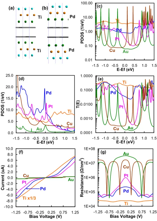
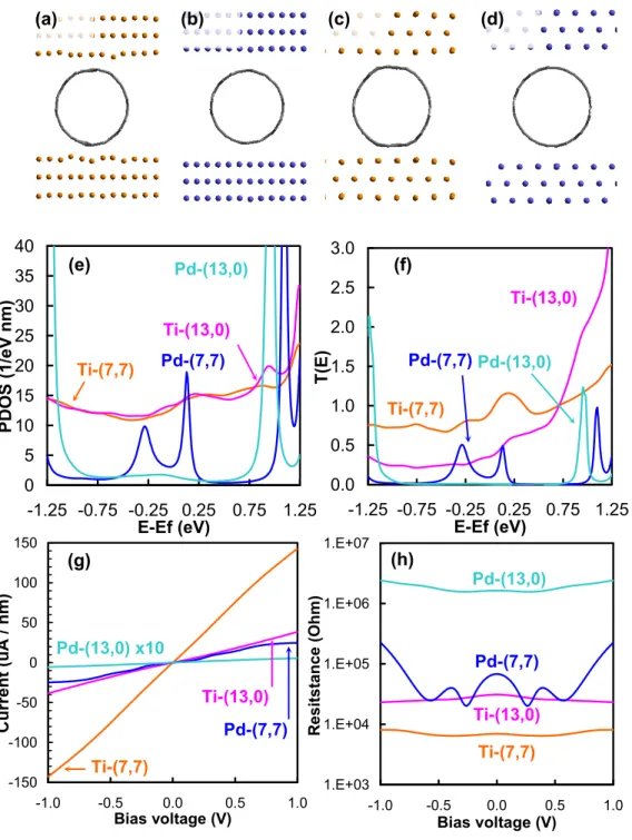
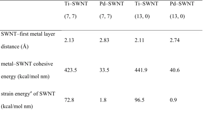
However, the high reactivity of the Ti electrode in contact with the nanotube distorts the nanotube structure. The PDOS and transfer functions of Ti– or Pd–SWNT (7, 7) are shown in Figures 3e and 3f, respectively.
Conclusion
M (r.t. in air)
Improving Contact Resistance at the Nanotube–Cu Electrode Interface Using Molecular Anchors *
Introduction
In this paper, our primary concerns are to improve the mechanical stability and contact resistance at the interfaces between CNT or SGS and other metals when building multi-level on-chip interconnects. Finally, we illustrate some of the synthetic strategies that may be useful for incorporating the Cu-anchored CNT elements into nanoelectronics.
Methods
- Modeling Details
- Choice of Anchors
- Computational Details
The model geometries were carefully optimized using the following steps: (1) Cu anchor models were optimized to find the most stable binding sites and molecular species of the anchor molecules on the Cu(111) surface. The final V transmission T(E, V) should be close to T(E) at a low bias voltage of -0.1 to 0.1 V, which would be the range of device operation studied in this paper.
Results
- Optimization of Cu–Anchor Models
- Optimizations of Graphene–Anchor Models
- Optimization of Cu(111)–Anchor–Graphene Models and Construction of I–V models
- Contact Resistance of Cu(111)–anchor–graphene Models
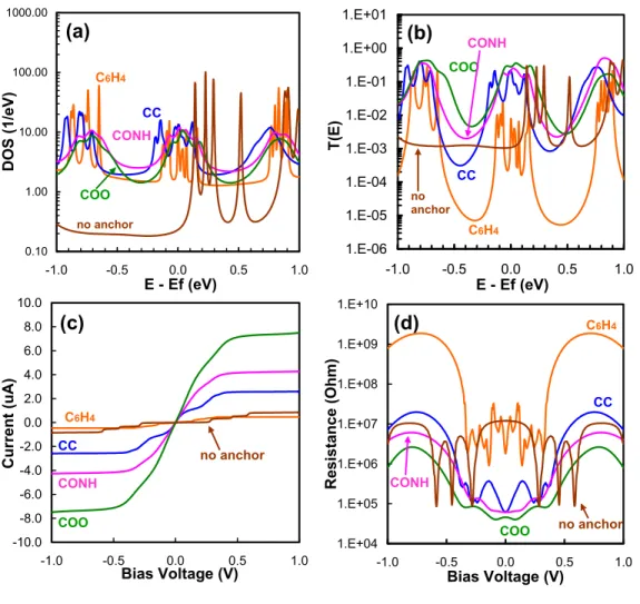
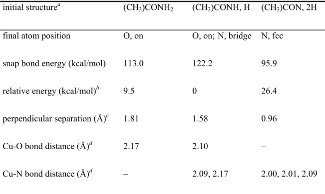
One hydrogen atom is placed on the Cu surface for the (CH)3CONH model, and two hydrogen atoms are placed on the Cu surface for (CH)3CON to allow comparison of the total energies of all models. The results clearly show that the addition of other anchors in the resonance position stabilizes the overall graphene-anchor models.
Discussion
- Mechanical Stabilities and Electrical Enhancements by Choice of Anchors
- Outline of Proposed Process Steps
There have been studies that have reported ways to implement CNTs at a specific location on the wafer by functionalizing the CNTs14, 15 or by functionalizing the substrate surface31 or both16. This step should be easily accomplished as there have already been experimental reports of.
Conclusion
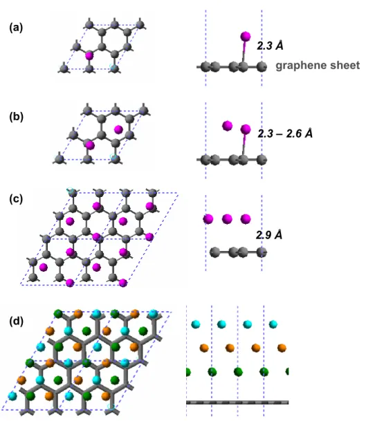
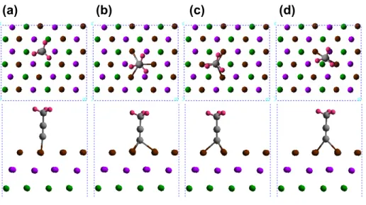
Additional support for the MSC was provided by ONR, ARO, DOE, NIH, Chevron, Boehringer-Ingelheim, Pfizer, Allozyne, Nissan, Dow-Corning, DuPont, and MARCO-FENA. a) Cu anchor-graphene configuration for our simplified simulation model. Side views of I-V computational models built from the optimized Cu(111) anchor graphene models by flipping one of the models and placing it on the AB stacking positions of the original graphene sheet.
Proposed Steps for Forming Cu–Anchor–CNT Interconnect
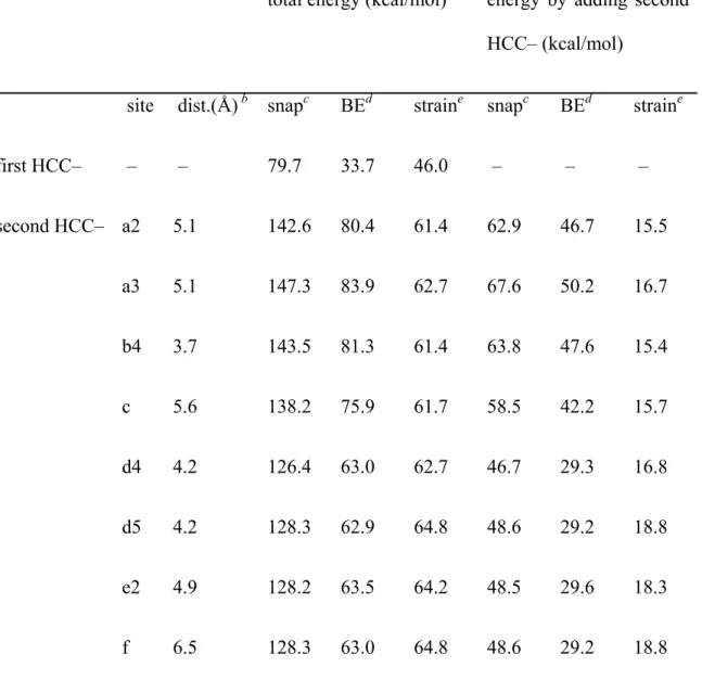
Adiabatic and snap bond energetics measured by addition of acetylene anchors (HCC–) per graphene unit cell nm2). The difference in the snap and adiabatic bond energies of two acetylenic (HCC–) anchors in resonant (a, b, c) and non-resonant (d, e, f) positions.
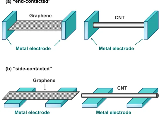
Contact Resistance of “End-contacted” Metal–Graphene and Metal–Nanotube Interfaces *
Computational Details
Ernzerhof flavor (PBE) of the generalized gradient approximation (GGA) with pseudo-atomic PBE potentials and within 2D periodic boundary conditions.29 k-point sampling of 4 × 4 in the Brillouin Zone and real space grid spacing of 46 × 26 in the plane x–y, for a grid spacing of 0.35 bohr, were carefully determined by energy convergence. To obtain the I–V characteristics of each model, the density of states (DOS) is obtained from quantum mechanics DFT, while the transmission coefficient is obtained using matrix Green's function theory with DFT (which we have successfully used to calculated the transport properties of the device molecular electronics).30 The transmission function was then used in the Landauer–Buttiker formula to calculate the I–V characteristics. The T(E, V = 0) zero-bias transmission approximation was applied to the calculation of the current I at a finite bias voltage (V) which was defined as the difference between the source and drain voltages.
The finite V transmission T(E, V) should be close to T(E) at a low bias voltage of –0.1 to 0.1 V, which would be the operating voltage range for devices studied in this paper. We then calculated the current as a function of the bias voltage and the contact resistance for the five deposited metals.
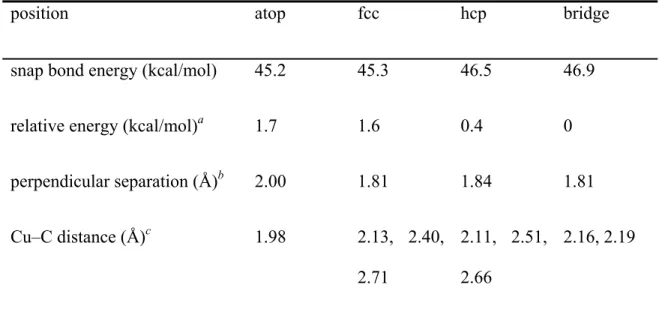
Geometrical Properties
These quantities were normalized by the surface carbon atoms at the interface (there are four carbon atoms). The structures for the I–V calculations ( Figure 4a ) were built from the optimized geometries ( Figure 2 ) by reversing the electrodes and the two surface layers of graphene carbon to calculate the contact resistance directory (Rcont). Notably, only d-orbitals of surface metals and p-orbitals of surface carbon atoms contribute significantly to the DOS (Figure S1).
The expected density of states (PDOS) per unit cell of p orbitals (PDOS(Cp)) of surface carbon atoms of graphene at the interface is shown in Figure 4b. Still, the PDOS(Cp) are large and uniform at the Fermi energy from 1.8 eV-1 (Ti) to 2.2 eV-1 (Au), indicating a good conduction channel. For the Ti, Pd, and Pt structures, the PDOS(Cp) of surface carbon atoms near the Fermi energy are mostly carbon pπ orbitals (py orbitals in Figure S1), but for the Cu and Au structures, both pπ- and pσ orbitals (py and pz orbitals in Figure S1, respectively) contribute equally.
The PDOS for the d orbitals of the surface (first layer) metal atoms (PDOS(Md)) are shown in Figure 4c. The transmission function, T(E), (Figure 4d) near the Fermi energy reflects the PDOS behaviors with the exception of the Cu system, which shows a lower T(E) than the Au system at the Fermi energy (-0.5 to +0, 25 eV).
Nature of the Metal–Carbon Contact
All contact resistances are also shown per surface carbon atom at the interface, allowing us to estimate the contact resistance of "end-contacted" metal-CNT interfaces, as will be discussed later.
Electrical Properties at the Interface
Pt−SWNT (10,10) interface will be Rend-cont =3.7 kΩ, indicating that "end-contacted" Pt electrodes can achieve the same contact resistance with "edge-contacted". The "end-contacted" electrodes are therefore more effectively used for multi-walled CNTs and CNT bundles. Despite the advantages of "end-contacted" configurations, there remain significant experimental problems with their construction.
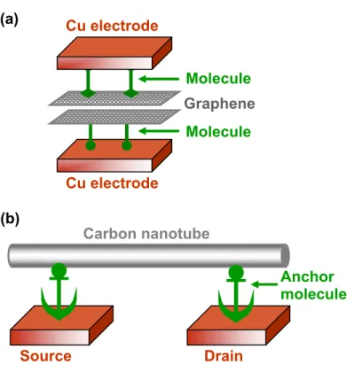
1/Rend-cont + 1/Rside-cont)-1, where Rend-cont = Rcend-cont / Nend-cont coming from the end-contacted interfaces and Rside-cont = Rcside-cont / Nside-cont coming from is from the “side contacts”. We analyzed the recently reported experimental contact resistance of Pt-CNT in comparison to our previous "side contact" calculations. Because of the difficulty in making “final contact”. electrodes as in Figure 1a, we propose Figure 6 as practical configurations that also dramatically reduce the overall contact resistance.
Although the application here is aimed at high-performance on-chip interconnect applications, the results should be applicable to other CNT or graphene based ones. nanoelectronic and optoelectronic devices such as the field effect transistors and light emitting diodes. a) Interaction energy of the metal-graphene "end-contacted" interface shown in Figure 1a. The layer-layer distances are given in Table 1 (C, graphene layer at the interface; M1, metal layer at the interface (first layer); M2, second metal layer; M3, third metal layer; M4, fourth metal layer). a) Interaction energy (per surface C atom) of the metal–graphene for “end-contacted” interface shown in Figure 1a, and (b) for “side-contacted” interface shown in Figure 1b (Ref. 24).
Definitive Band Gaps in Single-Walled Carbon Nanotubes*
Computational Methodology
To determine the structural parameters, we used the Graphite Force Field9, which leads to the exact properties of fullerene and CNT molecules and crystals.10,11 CNT geometries were fully optimized without symmetry constraints. For band calculations, we used CRYSTAL12 software based on Gaussian basis sets with periodic boundary conditions.
Results and Discussion
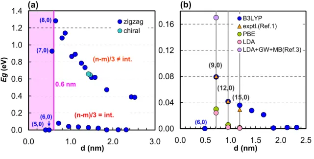
When d > 0.6 nm, the band gaps of zigzag SWNTs which are semiconductors decrease according to the chiral vector rule (n mod 3 ≠ 0) as the diameter increases. The reasons supporting the presence of small band gaps are due to the intrinsic properties of the SWNTs and not due to other effects such as distortions at the measurement conditions of very low temperature (~5 K), ultravacuum and an Au(111) ) substrate. As the allowed k-points cross closer to the K-points with larger diameters, the effective masses and band gaps decrease.
In addition, we also show the band gaps and effective masses are inversely proportional to the diameter squared at d > 1.3 nm. Band gaps (eg) of “Metallic” ((n – m)/3 = integer) Zigzag and chiral SWNTs using B3LYP functional compared to experimental, PBE and LDA gaps. Structural parameters after the force field optimization and the band gaps of Zigazag, armchair and chiral SWNTs calculated using the B3LYP functional.
According to the chiral vector rules, (12,0) and (15,0) are metallic, but there are small band gaps at the Fermi energy, as shown in Figure 2. According to the chiral vector rules, (18,0) and ( 21.0) are metallic but there are small band gaps at the Fermi energy as shown in Table 2.
Surface Properties of H–SiNWs
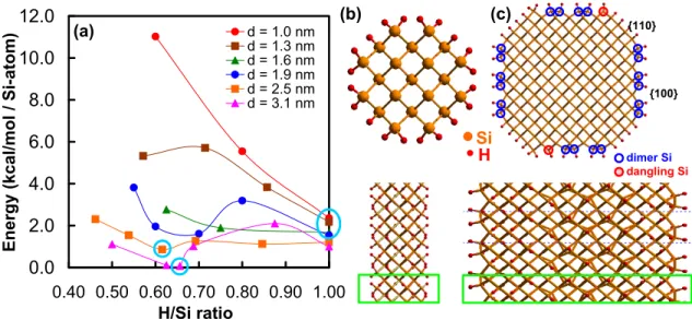
At the corners of these 8 plateaus, we find that Si atoms bond to one or two H atoms. For each optimized H–SiNW structure, heats of formation were calculated based on the energies of the plurality of Si and hydrogen molecules. The results are shown in Fig. 1a as a function of the calculated H/Si ratio, where H and Si are the total number of atoms in the unit cell.
We measure this ratio for each diameter so that the fully saturated case has H/Si =1. This has twelve surface Si atoms per unit cell, with the central Si atom having one H atom and the corner Si atoms having two H atoms. Removal of four H atoms per cell from the saturated SiNW leads to an optimized H–SiNW (H/Si = 0 .80, Si21H16), which has two Si–Si dimers with H terminations at two corners and Eh = 5.5 kcal/mol.
It has ten Si dimers linked along the {100} sidewalls with two dangling bonds at the corners and saturated terminations on the {110} faces. H binding to these two dangling bond states increases the energy by 0.95 kcal/mol and is due to Si strains and H–H interactions.
Electronic Properties of H–SiNWs
The PDOS of the α and β spin electrons show that the four dangling bonding Si atoms lead to localized surface states for the HOMO and LUMO inside the band gap. Without the HOMO and LUMO in these NWs created by the surface dangling bonds, the band gap is 2.3 eV. The overestimation of the band gaps in small diameter H–SiNWs is expected using EMA.46.
Clearly, the dependence of band gap on diameter from the experiment is dramatically inconsistent with all QM calculations. We find that the dangling Si atoms lead to new LUMO and HOMO states in the band gap. a) Calculated H-SiNWs band gaps using B3LYP. The expected direct band gap due to quantization in the effective mass approximation for saturated H-SiNWs by assuming a square d x d well (blue, Eq.
We find that the four dangling Si atoms lead to new LUMO and HOMO states in the band gap. Note that the band gap is 0.39 eV, which is 1.3 eV smaller than the UB3LYP calculation shown in Figure S5.