Integration of Dye Lasers and
Microfluidics for Biochemical Analysis
Thesis by Yan Chen
In Partial Fulfillment of the Requirements for the Degree of
Doctor of Philosophy
California Institute of Technology Pasadena, California
2009
(Defended July 18th, 2008)
2009 Yan Chen All Rights Reserved
Acknowledgements
The six years at Caltech have been the most memorable time in my life so far, I owe many thanks for my experience here. First of all, I would like to thank my advisor, Prof.
Axel Scherer, for providing me with the opportunity and resources to complete my Ph.D. at Caltech. I am grateful to his guidance and support through all these years. His broad perspective, valuable advice, and sincere mentorship have always been a source of inspiration and motivation.
I would also like to thank my committee members: Prof. Changhuei Yang, Prof. Oskar Painter, Prof. Yu-Chong Tai, and Prof. Chin-Lin Guo, and other members in my candidacy committee: Prof. Mory Gharib, and Prof. Mladen Barbic.
My great thanks go to my collaborators: Dr. Zhenyu Li and Dr. John Zhong. It has been great to work with Dr. Zhenyu Li, I am most grateful for all the helpful discussions and valuable advice from him. Collaboration with Dr. John Zhong in USC Medical School has been very fruitful and enjoyable. I thank him for providing many valuable resources for research, and being a great friend.
The Nanofabrication group is a great place to work and study. I would like to thank all the members in the Caltech Nanofabrication Group. I would first like to thank Dr. Zhaoyu Zhang, who helped me get started from the first day I arrived in the lab. I also benefit a lot from many of our former group members, Dr. George Maltezos, Dr. Saurabh Vyawahare, Dr. Tereal Neal, Dr. Koichi Okamoto, Dr. Michael Hochberg, Dr. Tom Baehr-Jones, Dr.
Emil Kartalov, and Dr. Joyce Wong. I am grateful to the remaining members of the Nanofabrication group for their support and help in the lab, and their friendship, Chris
Walker, Teresa Emery, Lin Zhu, David Henry, Michael Shearn, Uday Khankhoje, Guangxi Wang, Ting Hong, Jingqing Huang, and Sameer Walavalkar. I would like to thank our secretary, Kate Finigan, and our lab coordinator, Dr. Guy DeRose, who have been working hard to enable an efficient working environment for all of us. I have been extremely fortunate to work with so many wonderful people in my time at Caltech.
Finally, but most importantly, I am eternally grateful to my parents and my grandmother for their unconditional love, constant support and confidence in me throughout my life. Above all I owe my deepest thanks to Jiarui Han, for his tremendous love, encouragement, and support during the past six years, none of this could have been accomplished without him.
Abstract
This dissertation describes the study of two important aspects of integration in microfluidics: optics and biochemistry. In optics integration, two types of miniaturized dye lasers, namely the solid-state polymer dye lasers and optofluidic dye lasers were demonstrated. Both of the dye lasers possess a resonant cavity with circular grating geometry, and they are suitable to serve as low-threshold, surface-emitting coherent light source in microfluidic networks. The mass production and large scale fabrication of such low-cost dye laser arrays can be realized by the well developed nanoimprint and soft lithography, making this technology attractive for various biochemical applications. In biochemistry integration, a microfluidic system was developed to fully utilize the complexity of microfluidic circuits to process single cells and extract gene expression information in a parallel manner. The work presented here explored both the optics and biochemistry integration in microfluidics, which are the key issues for further development of complete “lab-on-a-chip” systems.
Contents
Acknowledgements ...iii
Abstract ... v
List of Figures ... x
List of Tables ... xv
Glossary of Acronyms ... xvi
1 Introduction ... 1
1.1 Overview ... 1
1.1.1 Optics in microfluidics ... 1
1.1.2 Biochemistry in microfluidics ... 3
1.2 Thesis organization ... 4
2 Modeling of Circular Grating Structure by Transfer Matrix Method ... 5
2.1 Introduction ... 5
2.1.1 Circular gratings ... 5
2.1.2 Transfer matrix method ... 7
2.2 Transfer matrix analysis ... 8
2.2.1 Maxwell’s equation ... 8
2.2.2 Transfer matrix method ... 11
2.2.3 Transfer matrix method coefficients ... 14
2.3 Simulation results ... 17
2.3.1 Index matching ... 17
2.3.2 Cavity resonance ... 19
2.3.3 Electromagnetic field plot ... 23
3 Nanoimprinted Circular Grating Dye Laser ... 25
3.1 Introduction ... 25
3.2 Materials ... 28
3.2.1 PMMA ... 28
3.2.2 Organic dye ... 28
3.2.3 Cytop ... 29
3.3 Laser cavity design ... 30
3.4 Fabrication process ... 31
3.4.1 Imprint mold fabrication ... 31
3.4.2 Laser chip fabrication ... 34
3.4.3 Nanoimprint process ... 35
3.5 Results and discussion ... 38
3.6 Summary ... 42
4 Optofluidic Circular Grating Dye Laser ... 43
4.1 Introduction ... 43
4.2 Materials ... 46
4.2.1 PDMS ... 46
4.2.2 PFPE ... 47
4.2.3 Laser dye and solvents ... 49
4.3 Laser cavity design ... 51
4.3.1 Circular grating distributed feedback structure ... 51
4.3.2 Flow channel design ... 53
4.4 Fabrication process ... 55
4.4.1 Mold fabrication ... 55
4.4.2 Laser chip fabrication ... 59
4.5 Results and discussion ... 62
4.6 Summary ... 65
5 Microfluidic Device as a Platform for Single Cell
Biochemical Analysis ... 66
5.1 Introduction ... 66
5.1.1 Microfluidic device as a platform for biochemical analysis ... 66
5.1.2 Significance of single-cell gene analysis ... 67
5.2 Design of microfluidic devices for single-cell analysis ... 69
5.2.1 First generation of microfluidic chip ... 69
5.2.2 Second generation of microfluidic chip ... 70
5.3 Materials and methods ... 72
5.3.1 Mold fabrication ... 72
5.3.2 Device fabrication ... 72
5.3.3 Microfluidic station ... 73
5.3.4 Synthesis of cDNA from hESCs... 74
5.4 Operation of microfluidic device ... 75
5.5 Results and discussion ... 77
5.5.1 Device efficiency ... 77
5.5.2 Gene expression of single hESC cells ... 80
5.6 Conclusions ... 82
6 Summary ... 85
Appendix A ... 87
Appendix B ... 90
Bibliography ... 93
List of Figures
2.1 Diagram of a circular grating resonator design. The scheme illustrates the second-order Bragg diffraction including (1) normal diffraction to the grating surface
(first-order) and (2) in-plane feedback (second-order) ... 6
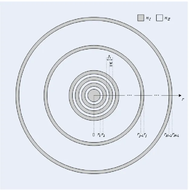
2.2 Schematic representation of a circular grating, with grating period , duty cycle w/ dc , effective indices nI and nII, cavity radius r1,r2,,rN1 ... 11
2.3 Effective index approximation of solid-state dye laser ... 28
2.4 Effective index approximation of optofluidic dye laser ... 17
2.5 The power ratio in circular grating with period of 440 nm for m=0,1,2 ... 19
2.6 The power ratio in circular grating with period varying from 400 nm to 450 nm ... 20
2.7 The power ratio in circular grating with two groove depths ... 21
2.8 The power ratio in circular grating with period varying from 400 nm to 440 nm ... 22
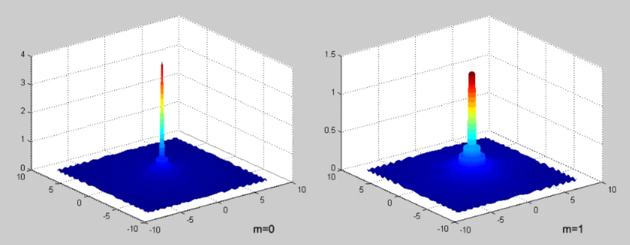
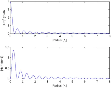
2.9 The 1-D graph of the normalized Hzj,m field in circular grating for m=0,1 ... 23
2.10 The 3-D graph of the normalized Hzj,m field in circular grating for m=0,1 ... 23
3.1 The general nanoimprint process... 26
3.2 Schematic diagram of a nanoimprinted circular grating dye laser chip ... 27
3.3 The monomer building block of PMMA ... 28
3.4 Rhodamine 640 molecule structure ... 29
3.5 Cytop molecule structure ... 29
3.6 General design of a circular grating distributed feedback structure ... 30
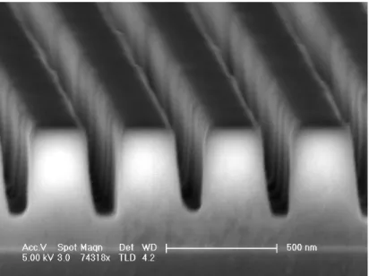
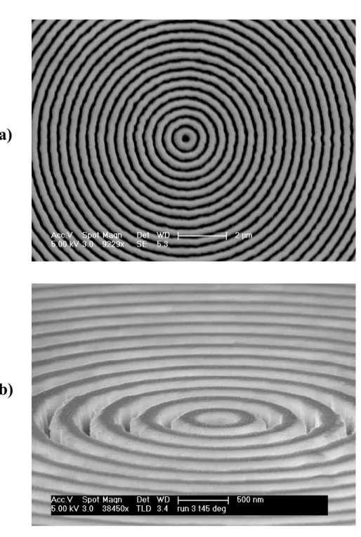
3.7 The SEM image of the cross section of an etched SiO2 grating ... 31
3.8 Schematic fabrication procedure for the circular grating nanoimprint hard mold. (a) The original wafer with 500 nm SiO2 on top of silicon substrate. (b) PMMA is spun on the sample for subsequent e-beam lithography steps. (c) The PMMA is exposed by b-beam, and the circular grating pattern is completely transferred into PMMA after developing the exposed resist. (d) The pattern is transferred into the SiO2 via CHF3 RIE etch, and the PMMA residue is removed after dry etch ... 32
3.9 SEM images of (a) the top view and (b) the angled view of SiO2 mold ... 33
3.10 Summary of the Cytop and PMMA substrate preparation process ... 35
3.11 Schematic nanoimprint process of circular grating polymer dye laser ... 36
3.12 SEM images of (a) the SiO2 mold and (b) the imprinted PMMA film ... 37
3.13 Measurement setup for polymer dye laser device ... 38 3.14 Nanoimprinted circular grating DFB dye laser spectrum. The measured linewidth is 0.18 nm. Inset: Polymer laser chip excited by Nd:YAG 532nm laser pulse ... 39 3.15 The output laser power vs. the absorbed pump energy curve. The threshold pump fluence is 1.31 μJ/mm2 ... 40 3.16 (a) Far-field image of the emission pattern recorded by a CCD camera. (b) Circular grating DFB laser far-field radiation patterns through a linear polarizer with different orientation angles ... 41 4.1 Schematic diagram of an optofluidic circular grating dye laser chip ... 45 4.2 Rhodamine 6G molecule structure ... 49 4.3 Cross sections of stimulated singlet state absorption and emission for Rhodamine 6G
in ethanol ... 49 4.4 General design of an optofluidic circular grating DFB dye laser cavity ... 51 4.5 Illustration of the Bragg diffraction in the second-order circular grating. First-order
Bragg reflection induces coupling to vertical propagating waves, and second-order Bragg reflection leads to in-plane feedback ... 52 4.6 PDMS microvalves (push-down version). Source: www.fluidigm.com ... 53 4.7 Microscope graph of microfluidic flow channel. Left: flow channel covering the
grating area. Right: flow channel filled with dye solution ... 54
4.8 Schematic fabrication procedure for the circular grating hard mold. (a) The original wafer with 1 µm SiO2 on top of silicon substrate. (b) Cr is evaporated on the sample. (c) PMMA is spun on top of the Cr for subsequent e-beam lithography steps.
(d) The PMMA is exposed by e-beam, and the circular grating pattern is completely transferred into PMMA after developing the exposed resist. (e) The Cr underneath the exposed pattern is removed by wet etch, and the remaining PMMA is also
removed. (f) The pattern is transferred into the SiO2 via DRIE etch ... 56
4.9 The SEM images of the cross-section of etched SiO2 gratings. (a) A cut-away view of the gratings. (b) Deeply etched trenches in the circular grating structure ... 57
4.10 SEM images of (a) the top view and (b) the angled view of the SiO2 mold ... 58
4.11 Fabrication process of hybrid PFPE/PDMS laser chip ... 60
4.12 (a) SEM images of SiO2 mold. (b) ESEM images of PFPE replica ... 61
4.13 Measurement setup of optofluidic dye laser chip ... 62
4.14 Optofluidic circular grating DFB dye laser spectrum. Inset: The output laser power vs. the pump energy curve ... 63
5.1 20X single-cell mRNA extraction microfluidic device filled with food dye ... 69
5.2 32X single-cell gene profiling microfluidic device filled with food dye ... 71
5.3 The setup of the microfluidic device for single hESC mRNA extraction. (a) The system includes a microscope, a computer to control air pressure with pressure regulators, and a heating plate. (b) A typical microfluidic chip ... 73
5.4 Merged image of immunofluorescent-stained (Oct-3/4) and light microscope images from a pluripotent hESC colony ... 74 5.5 The process flow in the single-cell microfluidic processor ... 76 5.6 Measuring absolute molecule numbers of three genes in single hESC with multiplex
quantitative PCR ... 79 5.7 Expression of B2M, Nodal, and Fzd4 in single hESC ... 81
List of Tables
4.1 Refractive indices of PDMS-compatible solvents ... 50 5.1 Microfluidic device increasing mRNA capture and reverse transcription (RT)
efficiency ... 78
Glossary of acronyms
2D – Two-dimensional
DBR – Distributed Bragg reflector DFB – Distributed feedback
ESEM – Environmental scanning electron microscope FDTD – Finite difference time domain
FP – Fabry-Perot
FWHM – Full width at half maximum MIBK – Methyl isobutyl ketone OSA – Optical spectrum analyzer PL – Photoluminescence
RIE – Reactive ion etching
PMMA – Poly(methyl methacrylate) Q – Quality factor
SEM – Scanning electron microscope
Chapter 1 Introduction
1.1 Overview
1.1.1 Optics in microfluidics
The field of microfluidics continues to become an important area with novel applications in biotechnology [1]. The most important goal for microfluidics is to achieve a complete
“lab-on-a-chip” system, which is capable of performing biological and chemical experiments normally carried out in a standard full-size laboratory. While efforts are made to develop the microfluidic system to realize more functionality for various biochemical reactions, the integration of optical components into microfluidic systems becomes more and more indispensable.
Optical detection and spectroscopic analysis are important in most micrototal analysis systems (μTAS) [2]. Currently a majority of microfluidic systems are based on external light sources. However, the coupling of optical signals in and out of the devices, typically by optical fibers, remains one of the major challenges in integrated optics. By making on-chip light sources, we can eliminate the optics alignment, which greatly reduces the complexity of the system. Therefore, the integration of miniaturized active light sources such as lasers into microfluidic systems becomes an attractive approach for biological and chemical processes.
We are very interested in the miniaturization and integration of dye lasers into microfluidic systems because of their broadband tunablity, low cost, and easy fabrication.
Dye lasers have been widely used as tunable, coherent light sources for spectroscopic analysis in the visible wavelength region (from 400 nm to 900 nm) during the past 30 years [3]. Miniaturized dye lasers, which can be integrated in lab-on-a-chip microsystems, would similarly have numerous applications. For applications in biochemical analysis in microfluidic systems, a surface emitting laser is more useful than other lasers because of its stacked substrate structure. Therefore, we choose a circular grating structure as the laser resonator design to produce low-threshold surface emitting lasing. The laser operating characteristics can be significantly improved by the two-dimensional nature of the resonator structure.
Two types of miniaturized dye lasers with the circular grating geometry are demonstrated in this thesis: solid-state and optofluidic dye lasers. For the solid-state dye laser, the laser dye is doped in the polymer forming the laser resonator, and it is fabricated using nanoimprint lithography. For the microfluidic dye laser, the laser dye is dissolved in an organic solvent and flowed through a microfluidic channel with laser resonator embedded, and it is realized by soft lithography. They can produce high-intensity and narrow-linewidth lasing with a well-defined output beam.
The well developed nanoimprint and microfluidics technology provide a convenient way of mass production and large-scale fabrication of low-cost dye laser arrays with a wide wavelength output range. It is also straightforward to build on-chip dye lasers with waveguides to replace the optical fibers necessary for the integrated optics. The miniaturized dye lasers can serve as surface emitting coherent light sources, which are very important in various biochemical applications, such as laser-induced fluorescence and spectroscopy.
1.1.2 Biochemistry in microfluidics
As we study the optical integration in microfluidic systems towards fully functional
“lab-on-a-chip” system, we are exploring more capabilities of the microfluidic system in the field of biochemical analysis. Lab-on-a-chip devices have the potential to revolutionize biochemistry by allowing complicated biochemical procedures to be performed on a small microfluidic chip. Single-cell processing is one of the major applications of microfluidics that can take advantage of its nanoliter fluid handing abilities.
A microfluidic approach that can extract gene expression information from individual single cells is described in this thesis. The integrated process: cell capture/lysis, mRNA isolation/purification, and cDNA synthesis/purification for single human embryonic stem cells is implemented on a microfluidic device. With the improved design of the microfluidic circuit, a parallel processing of dozens of cells with 100% efficiency can be achieved.
The gene expression of human embryonic stem cells (hESC) is a critical aspect for understanding the normal and pathological development of human cells and tissues.
Current bulk gene expression assays rely on RNA extracted from cell and tissue samples with various degree of cellular heterogeneity. These “cell population averaging” data are difficult to interpret, especially for the purpose of understanding the regulatory relationship of genes in the earliest phases of development and differentiation of individual cells. Here, we report a microfluidic approach that can extract total mRNA from individual single cells and synthesize cDNA on the same device with high mRNA-to-cDNA efficiency. This feature makes large-scale single-cell gene expression profiling possible. Using this microfluidic device, we measured the absolute numbers of mRNA molecules of three genes in a single hESC. Our results indicate that gene expression data measured from the cDNA of a cell population is not a good representation of the expression levels in individual single cells. Within the G0/G1 phase pluripotent hESC population some individual cells did not express all of the 3 interrogated genes in detectable levels. Consequently, the relative expression levels, which are broadly used in gene expression studies, are very different
between measurements from population cDNA and single-cell cDNA. The results underscore the importance of discrete single-cell analysis, and the advantages of a microfluidic approach in stem-cell gene expression studies.
1.2 Thesis organization
The thesis is organized as follows: Chapter 2, Chapter 3 and Chapter 4 focus on the optics integration of the microfluidic system, and Chapter 5 highlights the biochemistry aspect of the microfluidic system.
Chapter 2 extensively studies the modeling of circular grating resonators using transfer matrix method. An analytical model is developed to locate the resonance in a circular grating resonator. Both the parameters from solid-state and optofluidic dye lasers have been applied to the analytical model, and the simulation results are compared with experimental data. Chapter 3 describes the fabrication of solid-state polymer dye lasers using nanoimprint lithography. The detection result of the surface emitting dye laser with a circular grating geometry is discussed. Chapter 4 presents the fabrication of optofluidic dye lasers using soft lithography. A hybrid material system is introduced to make functional microfluidic laser devices. Chapter 5 demonstrates the use of microfluidic system as a platform to perform single-cell gene analysis. Chapter 6 concludes the thesis with an outlook of the future work for integration of optics with microfluidics for various biochemical applications.
Chapter 2
Modeling of circular grating structure by transfer matrix method
2.1 Introduction
2.1.1 Circular gratingLaser (Light Amplification by Stimulated Emission of Radiation) is composed of a gain medium and a resonant optical cavity [4]. The gain medium amplifies the beam by stimulated emission, and the resonant cavity provides the feedback necessary for the lasing operation. For our solid-state and optofluidic dye lasers in Chapter 3 and Chapter 4, we choose the circular grating resonator as laser cavities for their unique two-dimensional nature and enhanced lasing performance.
In particular, we use the second-order circular grating distributed feedback (DFB) structure as the resonant cavity. The distributed feedback scheme indicates that the gain material is directly implemented in the grating structure. The circular grating DFB structure satisfies the second-order Bragg condition, Bragg neff, where Bragg is the emission wavelength, neff is the effective index of the waveguide mode, and is the grating period, with an inner cavity providing a quarter- or half-wavelength shift similar to the classical DFB case.
Figure 2.1: Diagram of a circular grating resonator design. The scheme illustrates the second-order Bragg diffraction including (1) normal diffraction to the grating surface
(first-order) and (2) in-plane feedback (second-order).
The second-order grating is used to obtain surface emission, because it not only couples counter-propagating radial waves (via second-order Bragg reflection), but also induces coupling of radially propagating waves into the direction normal to the grating surface (via first-order Bragg reflection). Fig. 2.1 shows a cut-away diagram of a typical circular grating resonator. The corrugations in the grating structure provide both distributed feedback and output coupling of the guided optical mode via second-order and first-order Bragg scattering.
2.1.2 Transfer matrix method
To understand the resonant behavior of the circular grating, a theoretical analysis is necessary. There are many methods for modeling circular optical resonators. Most of the models are based on couple mode theory [5-9], which is more suitable for analyzing circular grating structure with shallow trenches and a modest light confinement. In this chapter, we present a transfer matrix method for analyzing circular grating structure with deep etched trenches. The deeper trenches of the structure lead to stronger in-plane effective index modulation, therefore the resonator can confine light in a smaller volume.
The transfer matrix method [10] is a straightforward method for analyzing optical structures composed of an arbitrary number of dielectric layers. When the dielectric properties are taken into account and the boundary conditions are satisfied, a transfer matrix can relate the electromagnetic field on either side of an optical region. Therefore, a complex structure can be modeled by simple matrix multiplication of basic subcomponents.
The transfer matrix method is suitable to analysis of various resonant optical cavities, such as multi-section Fabry-Perot, DBR, DFB, and VCSEL geometries [11]. For our application, we are interested in utilizing transfer matrix method for the analysis of structures with cylindrical symmetry.
In this chapter, we derive a transfer matrix method appropriate for description of the optical modes of circular grating microcavities. The electromagnetic modes of cylindrical multilayer structures are analyzed in terms of propagating waves, i.e., Hankel functions. In this chapter, the theoretical analysis follows the calculations of [12] and [13]. Using this transfer matrix method based 2-D cylindrical model, the spectrum information of the cavity modes can be obtained to analyze the energy confinement in the circular grating structure.
2.2 Transfer matrix analysis
2.2.1 Maxwell’s equationTo solve the wave equation, we define E
and H
as the vector electric and magnetic fields in the circular grating structure, and they are represented by (Ez,Er,E) and
) , ,
(Hz Hr H in cylindrical coordinates. In our 2-D model, we simplify the circular Bragg grating to infinite cylinders, and consider the system invariant in the z direction. Therefore, the electrical field and magnetic field can be expressed as E(r,)eit
and H(r,)eit . The Maxwell’s equation is given below in its differential form
0 0
H E
E i H
H i E
(2.1)
where and are the magnetic permeability and dielectric permittivity in the grating structure, and is the angular frequency of the electromagnetic field.
At all layer interfaces, the tangential components of the electric and magnetic field E and H
must be continuous. The system is invariant in z direction, therefore the solutions can be decomposed into two distinct polarizations: transverse electric (TE) and transverse magnetic (TM). We need to explore the general solutions of the Maxwell’s equations for the cylindrical symmetry, i.e., Hankel functions, and use them to solve the optical modes based on the transfer matrix method.
We can derive the Helmholtz equation from Maxwell’s equation and solve it for the cylindrical coordinate.
2 2
0
H k E
(2.2)
where k is the wavenumber in the grating structure and satisfies k2 2. Expressing the Helmholtz equation in cylindrical coordinates, we have
1 0 )
1 ( 2
2 2 2 2
2
H k E z r
r r r
r
. (2.3)
Because the system is invariant along the z coordinate, the separation in z components and in a transversal part is possible. Let k2 kT2 kz2, where kT and kz represent the component for the polar and z coordinates, respectively.
If we apply the following variable separation to Eq. (2.3),
) ( ) ( )
, (
) ( ) ( )
, (
r R B r
H
r R A r
E
z
z (2.4)
the equation becomes
0 ) ( ) ) (
( ) ( ) ( )1 ) (
) (
( 2 2
2 2 2
2
R r kT
r r R r
r R r r
r
R
. (2.5)
The equation can be separated into two parts with only dependence on r and , and each part can be solved on its own.
2 2
2 2 2 2
2
2 ( )
) ( 1 )
( ) ( ) ( )
( r k m
r r R r R
r r
r R r R
r
T
(2.6)
The solution of ( ) 2 ( ) 0
2
2
m is either
eim
l m
m
l m m
) (
) ( ),
sin(
) (
), cos(
) (
12 . (2.7)
The equation below is known as the Bessel differential equation
0 ) ) (
( ) ( ) ( ) (
2 2 2 2
2
2
r k m
r r R r R
r r
r R r R
r
T . (2.8) Therefore, the general solution of the time harmonic electromagnetic field is the Hankel function, which is a linear combination of Bessel and the Neumann function,
) ( )
( ) (
) ( )
( ) (
) 2 (
) 1 (
r iN r J r
r iN r J r
m m
m
m m
m
(2.9)
) 1 (
m and m(2) are the first-kind and second-kind Hankel functions, respectively, m is the azimuthal order, Jm is the Bessel function, and Nm is the Neumann function.
The solutions of variable separated equations can be inserted into Eq. (2.4),
for the TE mode,
0
) 2 ( )
1
( ( ) ( )]
[ )
, (
m
im m
m m
m j
z r r r e
H . (2.10)
for the TM mode,
0
) 2 ( )
1
( ( ) ( )]
[ )
, (
m
im m
m m
m j
z r r r e
E . (2.11)
2.2.2 Transfer matrix method
The schematic circular grating laser structure is shown in Fig. 2.2. The circular grating structure consists of N infinite cylindrical concentric layers. Each layer consists of alternating dielectric materials with refractive indices nI and nII.
Figure 2.2: Schematic representation of a circular grating structure, with grating period, duty cycle dc w/, effective indices nI and nII, cavity radius r1,r2,,rN1.
Our goal is to describe the field propagating in a cylindrical waveguide structure shown in Fig. 2.2. Due to the 2-D nature of the problem, the field solutions can be decomposed into TE and TM polarizations, for which the field in the plane is entirely characterized by (Hz,Er,E)and )(Ez,Hr,H , respectively. The present cylindrical geometry suggests we expand the fields using first-kind and second-kind Hankel functions,
) 1 (
m and m(2), which are linearly independent and represent the inward and outward propagating circular (Hankel) waves.
We are mainly considering the TE polarization, since the perpendicular pumping light on the grating surface will cause almost pure excitation of TE waves [23]. As described in the previous chapter, the general TE solutions of the Maxwell’s equations in each layer j can be expressed as a linear combination of m(1)(njk0r)eim and m(2)(njk0r)eim for each mode m0,1,,, nj is the effective refractive index in each layer j.
The H-field is expressed as
0 , 0
0 ) 2 ( 0
) 1 (
) (
)]
( )
( [
) , (
m
im m
j z m
im j
m j m j
m j m j
z
e r H
e r k n r
k n r
H
. (2.12)
Based on Maxwell’s equations, H 0nj2iE,
j j r j
j z j z j
z
E E i n r
H H H
r z
0 /
/ 0 0
0 /
/ /
2
0 (2.13)
0 ,
0 0
) 2 ( 0
) 1 ( 2
0
) (
)]
( )
( 1 [
) , (
m
im m
j r
m
im j
m j m j
m j m j
j r
e r E
me r k n r
k i n
r n E
(2.14)
0 ,
0 0
) 2 ( 0
) 1 ( 0
) (
)]
( )
( [
) , (
m
im m
j m
im j
m j m j
m j m j
j
e r E
e r k n r
k c n
n r i
E
. (2.15)
) 1 (
m and m(2) are the derivative of m(1) and m(2), respectively.
Similarly, for TM polarization, the E-field is expressed as
0 , 0
0 ) 2 ( 0
) 1 (
) (
)]
( )
( [
) , (
m
im m
j z m
im j
m j m j
m j m j
z
e r E
e r k n r
k n r
E
. (2.16)
Based on Maxwell’s equations, E 0iH,
j j r j
z j z j
z
H H i r
E E E
r z
0 /
/ 0 0
0 /
/ /
0 (2.17)
0 ,
0
0 ) 2 ( 0
) 1 ( 0
) (
)]
( )
( 1 [
) , (
m
im m
j r m
im j
m j m j
m j m j
r
e r H
me r k n r
k n r
H
(2.18)
0 , 0
0 ) 2 ( 0
) 1 ( 0
) (
)]
( )
( [
) , (
m
im m
j m
im j
m j m j
m j m j j
e r H
e r k n r
k ic n
r n H
. (2.19)
2.2.3 Transfer matrix method coefficients
At the interface between the jth and (j1)th layers, located at rrj, the tangential fields components (Ez,H for TM polarization; Hz,E for TE polarization) must be continuous. The coefficients calculations of Transfer Matrix below are based on TE polarizations.
) , ( )
, (
) , ( )
, (
1 1
j j z j
j z
j j z j
j z
r H r
H
r E r
E
(2.20)
The relationship between the coefficients (mj,mj), (mj1,mj1) can be expressed by
j m j m j
m j m
j m j m j
m j m
a b
b a
1 1
(2.21)
where amj,bmj are the complex conjugates of amj,bmj.
( ) ( ) ( ) ( )
1
) (
) (
) (
) 1 (
0 )
2 ( 0 1 ) 2 ( 0
1 ) 2 ( 0 )
2 (
0 )
1 ( 0 1 ) 2 ( 0
1 ) 2 ( 0 )
1 (
k r n k
r n k
r n k
r D n
b
k r n k
r n k
r n k
r D n
a
j j m j j m j
j m j j j m
m j
m
j j m j j m j
j m j j j m
m j
m
(2.22)
with the index ratio
j j
n n 1
,
) (
) (
) (
)
( 1 0 (2) 1 0 (2) 1 0 (1) 1 0
) 1
( n r k n r k n r k n r k
Dmj m j j m j j m j j m j j . (2.23)
For TM polarization, the only difference is the index ratio
1
j j
n
n .
We can obtain an overall transfer matrix relating the inner cavity to the outmost ring by multiplying the transfer matrices for each layer. For j1,2,,N1,
1 1
m m N N m
m N
m T
. (2.24)
The overall transfer matrix TmN takes the form
11 11 11 11
m m
m m N
m N
m
N m N
m N
m N m
N m N m N
m b a
b a a
b
b a
A B
B
T A (2.25)
with
1 0
0 1
1 1
1 1 1
m m
m m
m B A
B
T A . (2.26)
In order to find resonant modes, we can assume 1m m1, since every incoming wave can be considered as an outgoing one after crossing the z axis. The power in each layer j can be defined as Pmj mj 2 mj 2.
Therefore the ratio of the electromagnetic power confined in the center ring Pm1 to that in the outmost ring PmN is
2 2
1 2 1 2
1
N m N
m
m m
N m
m
m P
R P
(2.27)
1 1
1
1 1
1
) (
) (
m N m N m m N m m N m N m
m N m N m m N m m N m N m
B A A
B
B A B
A
(2.28)
with mN 2 mNmN, mN 2 mNmN, we obtain
2 1 2
2 1 2
2
2 N
m N m m N
m N m m N
m N
m A B A B
. (2.29)
So the Power ratio Rm between the center ring and the outmost ring can be expressed as the function of the wavelength by transfer matrix elements AmN and BmN,
2
1
N m N m m
B A
R . (2.30)
The power ratio can give us an estimation of the resonance peak of the cavity modes in the absence of any source input, which helps us to have a good understanding of the energy confinement in our circular grating structures.
We can also estimate the field in the microcavity with the assumption 1m m1 ,
1
1
j m j m
j m j m j
m j m
A B
B A
j m j m j m j m
j m j m j m
A B
B A
. (2.31)
Therefore, in the TE polarization, we can write the H-field as a function of AmN and BmN
( ) ( )
Re 2
) ( )
(
) ( )
( )
(
0 ) 1 (
0 ) 2 ( 0
) 1 (
0 ) 2 ( 0
) 1 , (
r k n B
A
r k n r
k n
r k n r
k n r
H
j m j m j m
j m j m j
m j m
j m j m j
m j m m
j z
. (2.32)
Similarly, in the TM polarization, we can express the E-field as
( ) ( )
Re 2 )
( (1) 0
, r A B n k r
Ezjm mj mj m j . (2.33)
2.3 Simulation results
2.3.1 Index MatchingIn order to introduce the finite vertical component of the waveguide grating into our transfer matrix formalism, we use the effective index approach. In this method, two characteristic cross sections, the groove and the tooth, form two different slab waveguides, providing effective indices nI and nII for the corresponding layers in our transfer matrix model.
The effective index approximation for the solid-state circular grating dye laser model is illustrated in Fig. 2.3. The laser waveguide consists of the top cladding (air), the dye-doped polymer film (PMMA), and the lower cladding (Cytop), with the refractive indices of na 1.0, nf 1.49, 34nc 1. , respectively. The variance between neff1 and
2
neff is caused by the different thickness of polymer film in the groove and the tooth.
Figure 2.3: Effective index approximation of solid-state dye laser.
In the solid-state circular grating laser structure, the core thickness (the polymer thickness) is 1 um, and the grating trench depth is 400 nm, which gives the thickness of the two slab waveguides as t1 1m and t2 600nm. We can calculate the effective index using the 1-D multilayer waveguide solver [14]. The effective index of the tooth section is
4791 .
1 1
neff , and the effective index of the groove section is neff2 1.3403.
Similarly, the effective index approximation for the optofluidic circular grating dye laser model is illustrated in Fig. 2.4. The laser waveguide consists of the top cladding (PDMS), the liquid gain medium (dye solution), and the lower cladding (PFPE), with a refractive index of nt 1.40, 54nd 1. , 34nl 1. , respectively. The thickness of the two slab waveguides can be assumed as t1 1.6 m and t2 1 m. The resulting effective index of the tooth section is neff1 1.5321, and the effective index of the groove section is neff2 1.4007.
Figure 2.4: Effective index approximation of optofluidic dye laser.
2.3.2 Cavity resonance
600 605 610 615 620 625 630 635 640 645 650 10-1
100 101 102
Wavelength []
Power Ratio [arb. units]
m=1 m=0 m=2
Figure 2.5: The power ratio in circular grating with period of 440 nm for m=0,1,2.
For the solid-state dye laser, the corresponding parameters are introduced to the transfer matrix method. We first choose the grating period to be 440, and the duty cycle to be 0.5.
The effective indices are nI 1.48 and nII 1.34, respectively. The overall diameter of grating is 200 µm, which gives the grating layer number N 250. In Fig. 2.5, we plot the power ratio between the center ring and the outmost ring for different modes m0, 1, 2. We observe a pronounced resonant peak at m1, but no peaks at m0 or m2.
550 560 570 580 590 600 610 620 630 640 650 10-1
100 101 102
Wavelength []
Power Ratio [arb. units]
=400
=410
=420
=430
=440
=450
Figure 2.6: The power ratio in circular grating with period varying from 400 nm to 450 nm.
Fig. 2.6 shows the resonance peak corresponding to circular gratings with period from 400 nm to 460 nm. From the simulation results we can see that the cavity resonant modes fulfill the second-order Bragg condition Bragg neff. The resonant peak for grating with a period of 440 nm matches very well with the experimental results in Chapter 3, which proves that the transfer matrix method is a powerful tool to reveal the spectrum information of the cavity modes.
580 590 600 610 620 630 640 10-1
100 101 102
Wavelength []
Power Ratio [arb. units]
600nm depth 400nm depth
Figure 2.7: The power ratio in circular grating with two groove depths.
For the optofluidic dye laser, the main different grating parameters are their effective refractive indic