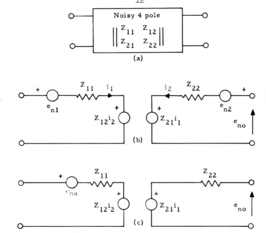
Formulation of equations describing the effect of temperature on the noise performance of the amplifier. The output signal-to-noise ratio is a function of (1) the noise generated in the driver impedance, and (2) the noise generated in the amplifier. T is the absolute temperature of s.. the source in degrees Kelvin, and B is the noise bandwidth of the amplifier.
To determine when the source signal-to-noise ratio and noise factor can be separately optimized, Equation 10 is differentiated. It is assumed that the signal-to-noise ratio of the source was maximum; optimization now includes noise factor minimization. However, now the noise voltage e shown in this figure is a function of the source impedance.
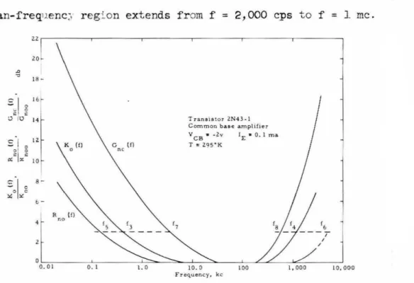
In order to obtain the noise factor as an explicit function of the emitter current, the physical sources of noise that exist in the transistor structure are investigated. An explicit configuration dependence is obtained by formulating the noise factor of the amplifier in each of its configurations. The frequency dependencies of the noise factor in the lower and upper transition regions are.
An expression for the noise factor [lUltistage of the system is then derived. Theoretical efficiency of the noise parameters as a function of 0:' Emitter current for the 2N43 transistor. With van der Ziel's mid-frequency noise model as a basis, it is possible to express the noise factor as an explicit function of the emitter current.
Equations 2-2a and 2-4 become the noise factor parameters of the common-base and common-emitter amplifier. With this assumption regarding the relative magnitude of R. s' becomes the noise factor of the common base and common emitter amplifier. The optimization process can be simplified by assuming that the noise sources in the model are not functions of the input termination.
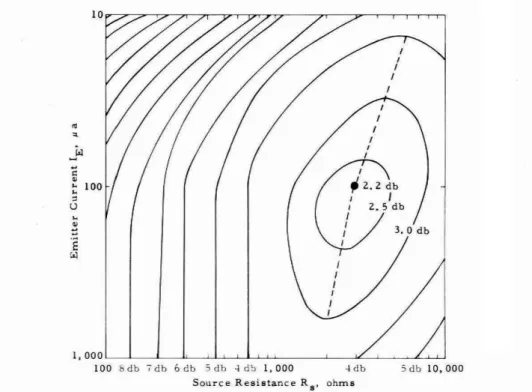
Any noticeable improvement in the noise performance of the amplifier can then be determined by a comparison of the respective noise factor parameters. So the minimum noise factor, which is written in terms of the noise factor parameters.
TEMPERATURE
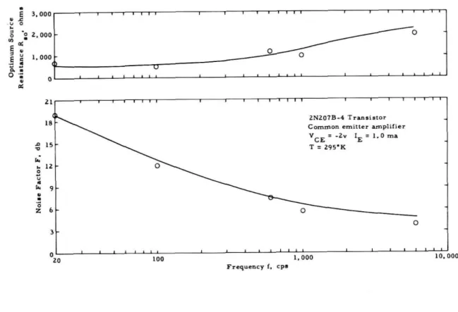
It is evident from the marked decrease in the magnitude of the optimization parameter, R , that the llf noise is observed at low tempera-. An explanation of this phenomenon can probably be found in the unfavorable temperature dependence of the common-base current gain, a. At larger values of emitter current, the recombination and diffusion generation noise generated in the active base region of the transistor plays a more prominent role in determining the value of R.
For typical values of the transistor parameters, TI is located in the range of 250 to 300o. A further analysis of the preceding equations shows that the minimum noise factor which, in terms of the noise-factor parameters, is given by However, this success is based on limitations regarding the size of the driving source resistance and the frequency of operation.
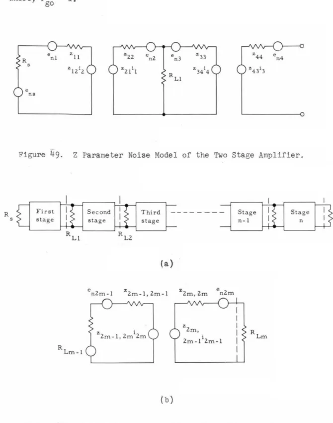
Middlebrook (Ref. 31) has shown that these stabilizing elements affect both the minimum noise factor and the optimum source resistance of the transistor amplifier. EFFECT OF BIAS VOLTAGE STABILIZATION ON TRANSISTOR AMPLIFIER NOISE PERFORMANCE Bias stabilization (shown in Figure 47a) is used to reduce temperature induced variations in the collector current of the common emitter amplifier.*. The rate of increase can be determined from an analysis of the noise model shown in Figure 47b.
With bias stabilization, dIe can be reduced to dICO'. a) Common-emitter transistor amplifier with bias stabilization, (b) noise model of bias-stabilized amplifier. The extent of this degradation can be determined from an analysis of the noise model shown in Figure 48b. a) Common-emitter transistor amplifier with emitter degeneration. (b) Noise model of amplifier with emitter degeneration. Only thermal noise is generated in the unbypassed emitter resistor. the noise factor parameters for the emitter degeneration stage become.
In contrast to bias stabilization, emitter degeneration increases the optimal source resistance of the transistor stage. The preceding analysis shows that both emitter degeneration and bias stabilization degrade the noise performance of the amplifier. The degradation produced by each is a function of the emitter current and the source resistance.
LOAD RESISTANCE AND MULTISTAGING
To determine whether an optimal load resistance exists, equation 7-1 is differentiated against R. L1•. Therefore, the deterioration of the sound performance of the two-stage system due to the load resistance of the first stage is a monotonically decreasing function of R. Equation 7-1 further shows that the load resistance degrades the sound performance of the two-stage system. ways. (which is represented by the second term in equation 7-1) and it magnifies (due to load) the effects of the noise sources present in the second stage. This is evidenced by the presence of RII in the third and fourth terms of equation 7-1.
With the first phase connected in the common-base configuration, the thermal noise can be neglected as the value of the load resistance. Thermal noise with the first phase connected in the common-emitter configuration can be neglected as. If the first phase is connected in the common-collector configuration, thermal noise can be neglected as.
To determine the effect on noise performance produced by loading the first stage, the common base common base amplifier is considered first. Ll, the noise generated in the second stage can never be neglected unless a step-up transformer is used between the first and second stages. The common collector-common collector (or Darlington) circuit will not be considered since a load resistor, RLl, is not needed in this configuration.
From this analysis, it is found that in the cb-cb and ce-ce two-stage amplifier, the noise performance degradation produced by RLl is mainly due to its loading effect on the second stage. For the cb-cb amplifier ~ should be made as large as possible; for the ce-ce amplifier need only exceed the value given by Equation 7-6. Extending the analysis to the multistage system, it is found that the noise factor of the mth stage of the amplifier (figure 5Ob) can be written as
For the transistor amplifier operated at frequencies well below a cutoff, it is safe to assume that. With this assumption, and the additional assumption that only thermal noise is generated in each of the load resistors, the noise factor for the n-stage system becomes
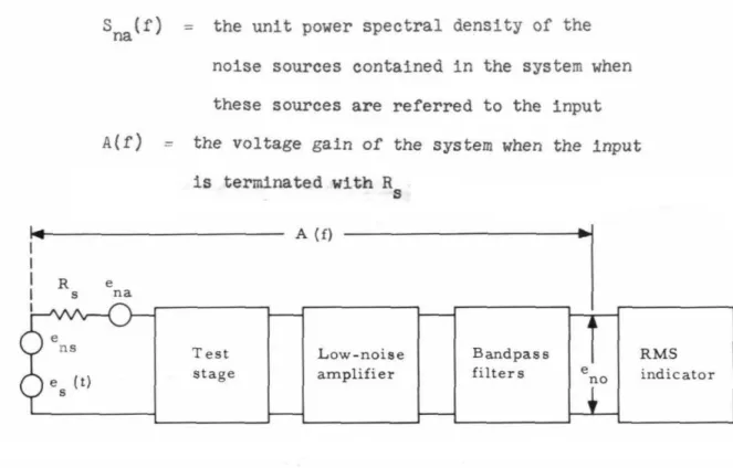
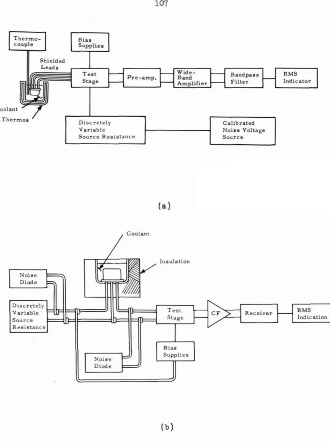
MEASURING METHODS
If B, the noise bandwidth of the system, is much smaller than f, the center frequency of the filters, Equation 8-1 is easier to read. In terms of the spectral densities, the noise factor is given by Sna(fo) + Sns(fo). To determine the noise factor of the amplifier using the CW method, the noise bandwidth B must also be calculated.
However, this part of the measurement procedure can be eliminated by using a noise current (or voltage). The noise current source that was used to obtain most of the average and high frequency measurements was the temperature limited diode. If the spectral density of the noise source, S , is assumed to be constant over an as yet undefined noise bandwidth, B .
In many of the noise measurements performed (particularly those at cryogenic temperatures), the noise added by the measurement equipment became a significant factor. That is, to obtain a true measure of mean square noise current (or voltage). Applying the sampling theorem to Van der Ziel's result shows that the probable error of the mean of M readings is 1s given by .
Assuming the noise bandwidth B = 4 cps and the time constant of the pointing device 't = 15 seconds, the probable reading error is 11% or 0.4 db. From this model, expressions were derived for the noise factor of the transistor amplifier in each of its configurations. An examination of the noise factor formulas reveals that in an unconstrained amplifier, ie. one in which the source resistance is not a fixed parameter, two quantities are important in determining amplifier noise.
However, the high-frequency noise cut-off point was found to be a function of the source impedance. Previous research has shown that in a two-stage rc-coupled transistor amplifier, the value of the load resistance of the first stage should optimize the noise factor of the second stage. They equalize if B, the noise bandwidth of the measurement system, is much smaller than the frequency at which the measurements are made.