Thank you to Jon for always sharing ideas and making science fun. Thank you to Heidi for your friendship and for keeping our morning swim fit.
NOMENCLATURE
INTRODUCTION
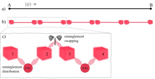
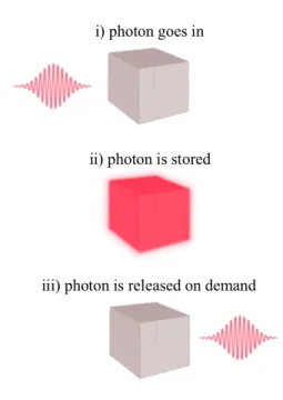
The Quantum Internet, Quantum Repeaters, and Quantum Memories A quantum memory for light is a device that stores light coherently for some portionA quantum memory for light is a device that stores light coherently for some portion
In the intervening years, many quantum storage protocols using groups of atoms have been proposed and realized [49]. In the absence of hyperfine states, spectral burning of holes can be achieved using Zeeman (electron spin rates).
Cavity Quantum Memories Using Nanophotonic Resonators
As described in this work, superhyperfine coupling limits the performance of AFC memories by limiting the minimum spectral feature. ZEFOZ transitions in 167Er3+:Y2SiO5 were not investigated in this work; we address them again in the Future Directions section of this thesis.
Structure of this Thesis
ERBIUM-167 IN YTTRIUM ORTHOSILICATE
- System Overview
- Optical Coherence
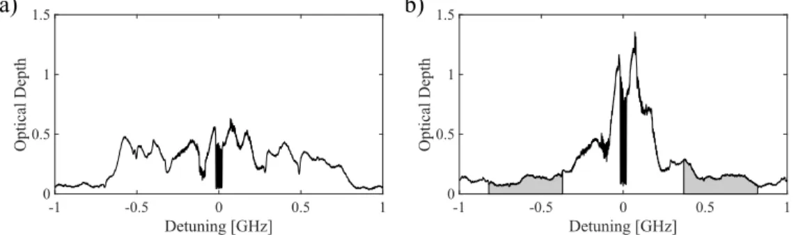
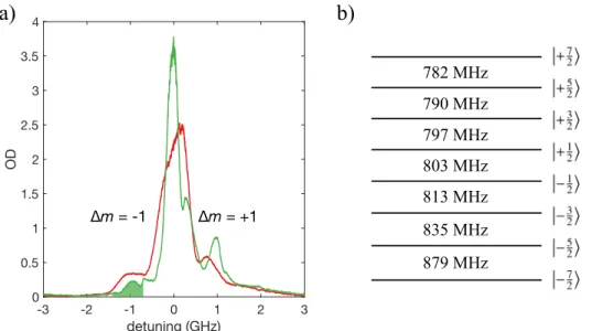
- Spectral Holeburning, Hyperfine Levels, and Initialization
- Superhyperfine Broadening
This effect leads to a small correction of the energy of the hyperfine levels and is usually ignored. Due to the low symmetry of the Y2SiO5 crystal, the magnetic field generated by the electron spin dipole moment is highly anisotropic, characterized by a rank 2 tensor ˆ𝑔[99].

ATOMIC FREQUENCY COMB STORAGE - THEORY
Storing Light in an Atomic Frequency Comb
Each term in the sum in equation 3.3 is represented as an arrow on the Bloch sphere. The diagram is in the rotating frame of the ions in the center of the comb (green). To create an atomic frequency comb in 167Er3+:Y2SiO5 in our experiments, a set of periodic spectral holes is burned into the absorption line after hyperfine initialization (see Section 2.3).
In AFC with a spin-wave protocol, after the input pulse (or input qubit) is stored at the optical gate, the optical 𝜋 pulse coherently shifts the population from the optically excited state to another long-lived spin state in the optical ground state of the splitter.

AFC Storage Efficiency in a Cavity
Note that this 𝛽 is very similar to the resonator mode energy fraction in the Y2SiO5 mode, 𝛽, defined in Eq. If the optical mode of the electric field component of the resonator is mainly aligned with the electric dipole moment of the ions, then. This relationship shows that the ensemble cooperativity scales linearly with the cavity quality factor and the optical mode fraction in Y2SiO5.
Note that the ensemble cooperativity is not measured by the number of ions associated with the cavity, but varies with the ion density, 𝜌ions ∼ 𝑁ions.
NANOPHOTONIC RESONATORS: DESIGN AND FABRICATION
Y 2 SiO 5 Nanobeam Resonators
Hybrid Amorphous Silicon-Y 2 SiO 5 Resonators
As shown in Figure 4.3, elliptical air holes are added to the 𝛼Si-167Er3+:Y2SiO5 waveguide in a periodic pattern to create a photonic crystal band centered at the design frequency of 𝜈◦ =195 THz. For the photonic crystal simulation, 𝑦 symmetry was also imposed to ensure that the first band gap was the fundamental TM mode (in this 3D simulation the electric field of the TM mode is along the 𝑧 axis). The difference in the 𝑘 values of the two modes leads to scattering between the photonic crystal and the waveguide.
The purpose of the taper is to adiabatically convert the Bloch mode of the photonic crystal into a TM waveguide mode.

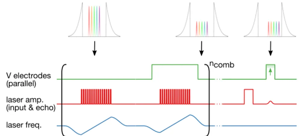
On-Chip Electrodes for DC Stark Shift Control
The purpose of the parallel configuration is to apply one electric field to all ions, which is represented by a delta function in figure. Therefore, the electric field does not change significantly in the 𝑧-direction, so only values at 𝑧 = 0 are shown. Similarly, there was no significant variation in the electric field in the 𝑦-direction across the 605 nm width of the optical resonator.
Electric field profile at 𝑦 = 0, 𝑧 = 0 for the parallel (a) and quadrupole (b) bias configurations of three electrode designs.

Coupling Between an Ensemble of Ions and a Cavity
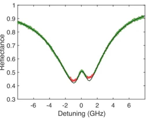
The resonator, which was introduced in section 4.1, increased the absorption of light by the ion ensemble, allowing on-chip implementation of the memory protocol [3]. The cavity was tuned to resonate with the 1539 nm transition of the 167Er3+ ions by freezing nitrogen gas on the nanobeam at cryogenic temperatures [82]. The coupling of the ensemble of ions to the cavity is seen as a peak in the cavity reflection dip.
For highly efficient storage using ions coupled to a cavity, the ensemble cooperativity should be equal to one (see Section 3.2).

Atomic Frequency Comb Storage
Section of the reflection spectrum of the resonator showing the atomic frequency comb at the center of the inhomogeneously broadened 167Er3+:Y2SiO5 transition. The apparent slope of the comb is due to its center frequency not being precisely aligned with the cavity resonance, leading to a dispersive shape. The black line also shows a partially reflected input pulse (𝑡 =0) and a smaller second output pulse at 𝑡 =330 ns.
Since this exceeds the comb period required for this storage time (Δ =1/𝑡storage =0.1 MHz), the resulting AFC will have lower contrast, leading to lower storage efficiency.
![Figure 5.2: AFC experiment in the nanobeam cavity (adapted from Ref. [30]). (a) A section of the resonator reflection spectrum, showing an atomic frequency comb in the center of the inhomogeneously broadened 167 Er 3 + :Y 2 SiO 5 transition](https://thumb-ap.123doks.com/thumbv2/123dok/10412826.0/61.918.267.623.104.523/experiment-nanobeam-resonator-reflection-frequency-inhomogeneously-broadened-transition.webp)
Coherent Storage of Time-Bin Qubits
Black lines fit a sum of cosine functions: each of the two combs with finesse𝐹 ~ 2 is approximated by a cosine function. The detuning of the second comb was swept from 𝛿2 = −0.2 MHz to 2.2 MHz, and the intensity of the two central overlapping output pulses was measured. Inset shows the four output pulses (middle two overlap) in the case of the maximum constructive (dashed black line) and maximum destructive (solid red line) interference.

Estimating a Lower Bound on Storage Fidelity
Of the three output time bins, the first and third were used for the measurement of 𝐹early and 𝐹late, while the second time bin was used for the measurement of 𝐹+ and 𝐹−, as shown in Figure 5.7. In all figures, blue (red) dash-dot represents the 60 ns time bins counted as 𝑁𝜓 (𝑁𝜙⊥𝜓).. The same dataset, shown in a) and b), was used for both the early and late fidelity calculations, since absolute time is irrelevant. The origin of this pulse was unclear, but it disappeared in the absence of the double comb.
𝑁photon standard deviation on all𝑁𝜓 values due to Poissonian statistics of photon count and the uncertainty, estimated at 15%, of the mean input photon counts, ¯𝑛.

Overcoming AFC Efficiency Limitation
Similar to the visibility curve discussed in Section 5.3 , the measured fidelity was limited in part by dark counts and in part by the dual-comb protocol being an imperfect interferometer. However, the AFC spin-wave protocol, where the stored information is reversibly transferred from the optical to the hyperfine manifold [4], would enable storage longer than 10𝜇s without the same requirements for narrow spectral functions, as well as enable on-demand recall. Following the analysis above, the subsequent set of devices used in the next chapter (Chapter 6) used a higher doping of 167Er3+ ions and resonators based on amorphous silicon waveguides on 167Er3+:Y2SiO5.
Nanobeam Device Temperature
To estimate the last two temperatures, the same pattern of laser pulses as in the actual experiments was sent to the nanobeam, at 0.3 nW and 0.02 nW, respectively, and PL was collected after the pulses. Assuming that the electron spin was in thermal equilibrium with the device, we therefore estimated the temperature of our device during experiments to be ~400 mK.
![Figure 5.8: Nanobeam device temperature measurement (adapted from Ref. [30]).](https://thumb-ap.123doks.com/thumbv2/123dok/10412826.0/70.918.277.611.107.517/figure-nanobeam-device-temperature-measurement-adapted-ref-30.webp)
DYNAMIC ON-CHIP CONTROL OF STORED LIGHT USING THE DC STARK SHIFT
Dynamic Control of Storage Time
Without electric field control, the largest emission, which we consider the output of the memory, will be at 𝑡 = Δ1 (𝑚 =1). Following reference [3], and using the notation of Section 3.2, the amplitude of the first output pulse from an AFC memory is:. The comb is created as in the first part of Fig. 6.2, then scanned by slowly changing the frequency of the laser using the piezo drive.
Because of the opposite sign between the two terms, the second emission becomes smaller as the first emission becomes larger.
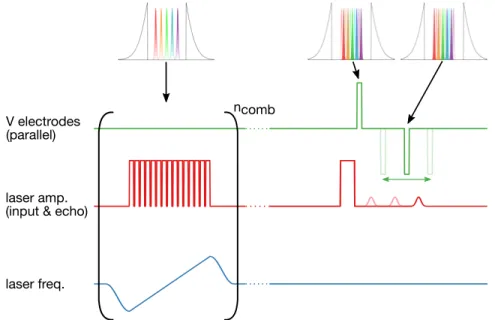
Frequency Shifting
Specifically, an electric field is chosen such that 𝛿 𝑓± =±Δ/4, where Δ is the period of the comb. The source of error is probably our calibration of the electric field (the 𝑥-axis in Fig.6.6c). The central blue band shows the expected frequency shift of the output pulse (or equivalently the ions that absorbed the input pulse).
This would result in partial absorption of the output pulse by the second subclass of ions and thus reduced storage efficiency.
Bandwidth Broadening
From the Gaussian fit of the output pulses, the temporal FWHMs (Δ𝑡) of the input and output pulses are extracted and converted to bandwidth or frequency FWHMs (Δ𝑓) using: Δ𝑓 = 4log2. The simple linear model described in Equation 6.7 does not fully capture the effect of the electric field gradient on the output bandwidth. Instead, the energy of the broadened output pulse is lower because AFC rephasing and rephasing due to the electric field gradient do not occur in the same time frame.
The figure shows the logarithm of the sum of the counters in the output time block at 𝑡 = Δ1.

Cavity-Ion Coupling and AFC Efficiency in a Hybrid 𝛼 Si-Y 2 SiO 5 Device In this section, we describe cavity-ion coupling and the AFC storage efficiency
To keep the number of equations to a reasonable size, the number of simulated ions 𝑛∼ 104 is significantly smaller than the true number of ions bound to the cavity ∼ 107. The cavity was tuned in resonance with the 1539 nm transition of free ions 167Er3+ gas in nanobeams at cryogenic temperatures [82]. In our setup, it was difficult to control the gas deposition rate, so the cavity usually ended up far in the red (high wavelength) after nitrogen gas tuning.
This is because a phased EOM is used to control the input frequency and only the positive sideband resonates with the cavity and ions.
Improving Efficiency in Hybrid Resonators
If we focus on the use of these types of devices for demonstrations in the near term, Figure 6.15 shows the resonator parameters needed to achieve a storage efficiency of 50%. If 𝛽 = 0.25 mode resonators are used, the quality factor requirements are slightly lower: 𝑄 =40×103, with an intrinsic quality factor of 𝑄𝑖 =220×103. The optical mode fraction in 167Er3+:Y2SiO5 is assumed to be mod =0.1. b) AFC efficiency versus internal quality factor𝑄𝑖 with mode 𝛽 = 0.25.
Assuming a solution for the superhyperfine coupling limit of comb burning, Figure 6.16 shows the predicted efficiencies for hybrid resonators using a comb finesse of .

CONCLUSION
Summary
Future Directions
Measuring these tensors would be useful to continue the work described in this thesis. In addition, the permanent dipole moment of the ground and excited states of v167Er3+:Y2SiO5 results in a linear DC Stark shift, which was used for dynamic control in this work. The superhyperfine spin coupling of the 167Er3+ electron to the yttrium core in this material also presents serious complications for AFC quantum storage.
Studies of new erbium-doped materials, such as the recent work by Phenicie et al., would be useful in this regard [83].
BIBLIOGRAPHY
Calculating Photonic Crystal Bandgap Using MPB
The code is in Scheme, compatible with the Scheme user interface in MPB (a Python interface is also available). The first column of the data is the wavenumber data in units of 2𝑘 𝑎𝜋, where 𝑘 is the wavenumber and 𝑎 is the unit cell dimension along the propagation axis. The following columns of the data are frequency in units of 𝑓 𝑎𝑐 , where 𝑓 is the frequency and 𝑐 is the speed of light.
Calculating Waveguide Band Diagram Using MPB
Calculating Reflectance of Mirror With Taper Using Comsol
FABRICATION PROCESS FOR ELECTRODES
MEASUREMENT SETUP FOR CHAPTER 5
LASER
Two Newport LB1005 servo controller boxes were used to feed back to the laser current and piezo voltage. An electro-optical phase modulator (EOM) was used to control the phase of the light or to add strong sidebands for hyperfine initialization. To drive the EOM, one of two RF sources was used: (1) a voltage controlled oscillator (Minicircuits ZX95-1300+) amplified using a JDSU H301-1210 amplifier or (2) the pulsed output of the random wave generator (AWG) .
A tuning line (1/4" copper tubing) directed toward the sample was used to spray nitrogen gas onto the resonator to tune its resonant frequency.
MEASUREMENT SETUPS FOR CHAPTER 6
Measurements with SNSPD
An aspherical lens pair, mounted on a stack of attocube𝑥 𝑦 𝑧nanopositioners, focused light from an optical fiber onto the grating coupling of the resonator. Trim coils on either side of the electromagnet offset the stray magnetic field along the crystal axis. Electrical pulses were sent to the chip (PCB board with SMP connector) via a coaxial chain with "0 dB" attenuators in each stage of the dilution refrigerator.
Visible are: the copper assembly connected to the mixing chamber plate (gold); the attocube nanopositioners with wiring; the optical fiber and the 1/2" lens tube containing the lens pair for coupling; the solenoid electromagnet; two magnet trim coils to the left and right of the solenoid; and the copper tuning line pointing to the sample.

Heterodyne Detection
For this reason, there are two paths that split and rejoin on the signal arm: a strong "input" arm and a weak comb burnout arm. The MEMS switch sends light through one of two paths during the experiment as needed.
Parts List