Introduction to metasurfaces
Introduction to optical metasurfaces
Over the past twenty years, the field of metasurfaces has made great progress. To overcome the limits of the plasmonic structures, various types of dielectric metasurfaces have been investigated.
High-contrast dielectric metasurfaces and their capabilities to control
If the metasurfaces are composed of the nanoposts with anisotropic cross-sections such as rectangles or ellipses, they allow the capabilities to control the polarization and phase simultaneously. In other words, the metasurfaces enable arbitrary two-dimensional distribution of the Jones matrices satisfying Eq.1.1.
Progresses and challenges in active metasurfaces
Recently, it has been shown that spatially varying Jones matrices enabled by metasurfaces lead to different types of spatially varying Jones matrices in the far field [44]. This design method is useful if metasurfaces are designed for output functions without a database of input polarization states.
Thesis outline
Single-shot quantitative phase gradient microscopy using a system
Introduction
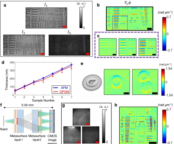
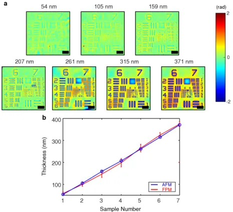
While conventional phase imaging methods such as phase contrast [57] and differential interference contrast (DIC) microscopy [58] capture only qualitative phase information, quantitative phase imaging (QPI) has grown rapidly over the past two decades. The first metasurface together with each of the lenses in the second metasurface layer forms a different image of the object.
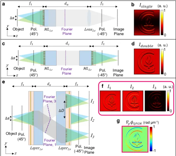
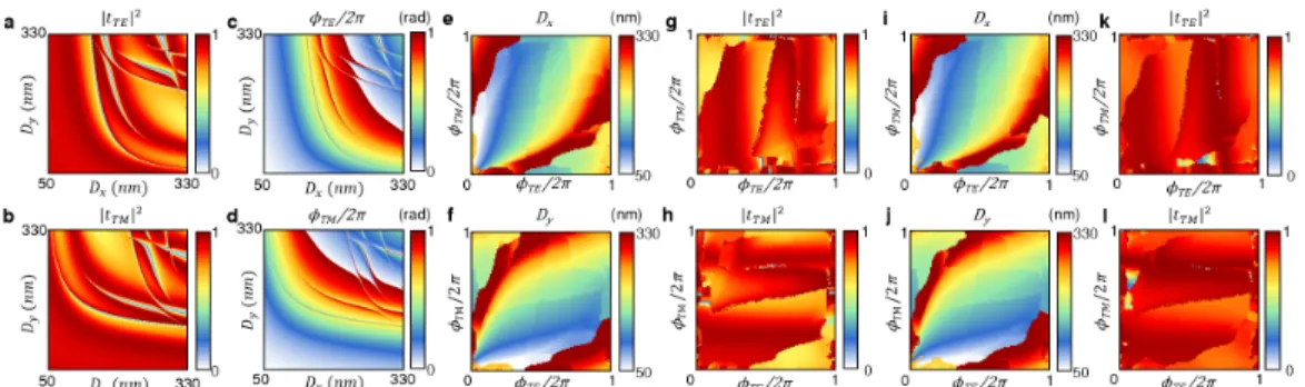
Concept of the metasurface-based QPGM
The QPGM consists of the two multifunctional metasurface layers for two main reasons (see Appendix 2.1 and Fig. 2.A.1 for detailed discussion based on wave propagation simulation). Second, the vertical integration of the two multifunctional metasurface layers enables unambiguous capture of the PGI in a single shot with compact implementation of the system.
Implementation of the QPGM by two separate dielectric metasurface
Imaging with the QPGM based on two separate metasurface layers . 14
Outlook and Summary
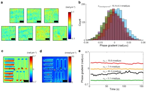
In addition, different focus scanning schemes can be integrated with the quantitative phase gradient microscope to achieve a tomographic quantitative phase imaging device with fast axial scanning. In conclusion, we used two multifunctional metasurface layers to realize miniaturized quantitative phase gradient microscopes.
Methods
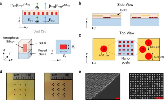
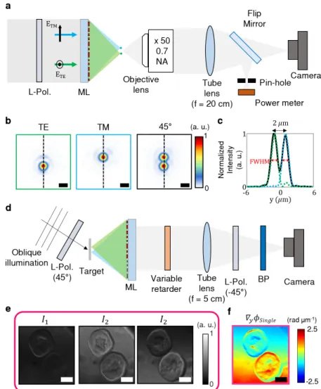
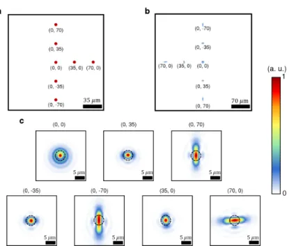
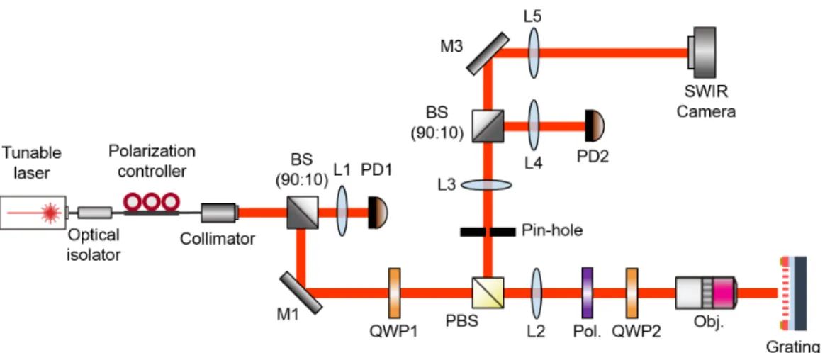
Two 664-thick layers of amorphous silicon were deposited on both sides of the substrate using a plasma-enhanced chemical vapor deposition technique. The imaging performance of the QPGM was characterized using the settings schematically shown in Fig. 1b.
Appendix
Computational complex optical field imaging using a designed
Introduction
For example, the instability of the optical properties [123], the fluctuation in the transmission of diffuse CSM [124], and the trade-off between memory effect range and maximum scattering angle range [125] could be critical disadvantages from a practical point of view. of view. These properties provide important insight into the optical properties of the MD as a scattering medium and clarify the required operating conditions of the SSM method.
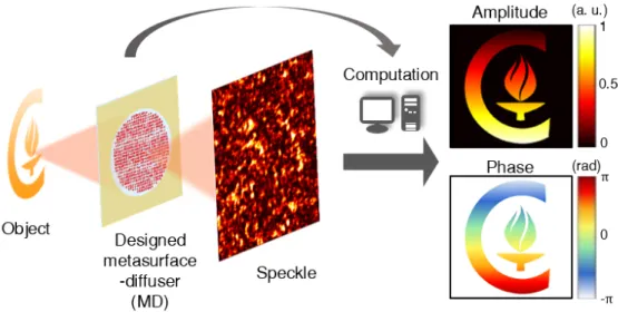
Metasurface diffuser design
To suppress the unscattered light power behind the MD (which is unavoidable due to the finite scattering efficiency and fabrication imperfections), we designed and operated the MD in a polarized configuration. The transmission phase of the two orthogonal polarizations can be manipulated using meta-atoms.
Theory and simulation results
As shown in Fig.3.3c, the distribution of the normalized eigenvalues of 𝑇†𝑇/𝑀 for MD deviates from the Marchenko Pastur law, indicating dependence between the entries of 𝑇 [141, 144]. To numerically investigate the operation of the MD, we performed simulations using amplitude and phase samples.
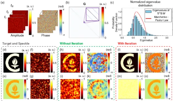
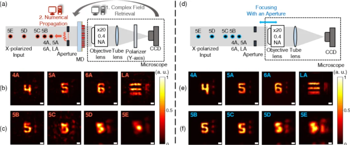
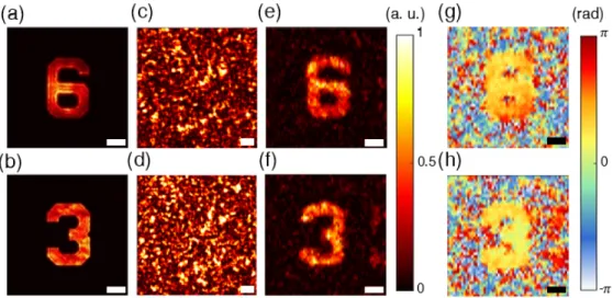
Experimental complex field retrieval with amplitude targets
Therefore, the reflectance spectra shown in Fig.6.2 are highly dependent on the input polarization capability.
Numerical noise tolerance analysis
Holographic imaging experiment and numerical analysis of robust-
The fields are then numerically back-propagated to the desired distance to reconstruct the object behind the aperture. In both Fig.3.6cand3.6f, the image resolution decreases as the object distance to the aperture increases. The field is then back-propagated to reconstruct the object at different distances from the aperture.
Discussion and conclusion
We have also numerically investigated the performance of MD and the method under axial and transverse displacements. The method is not only robust to the MD displacement in the axial and transverse directions, but also some misalignments can be corrected or exploited in the alignment of the optical system (see Section S3 and Fig.3.A.10 for details). CSM usually suffers from the trade-off between the light efficiency and the maximum scattering angle, because both are highly dependent on the thickness of the CSM.
Methods
Appendix
Introduction
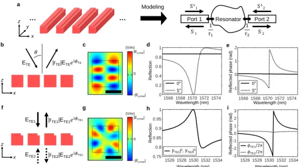
Both the GMR and the quasi-BIC modes are not only highly resonant but also efficiently coupled to free-space modes. In contrast to the devices that host a single GMR mode, devices that host both the GMR and the quasi-BIC modes can be advantageous in exhibiting a larger phase response. It is also shown that the electrical tuning of the interference between the GMR and the quasi-BIC mode can provide continuous tuning with large phase response.
Results
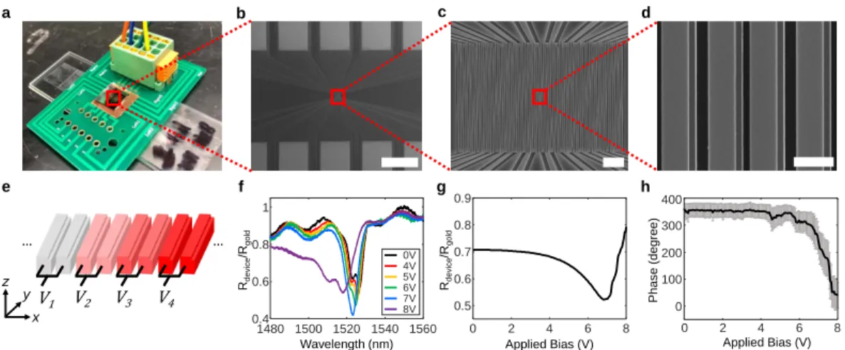
In b and c, black and red circles indicate resonances of the GMR and quasi-BIC modes, respectively. The optical image of the fabricated device and printed circuit board is shown in Figure 4.1d. The black and red circles show the positions of the GMR and quasi-BIC modes, respectively.
Summary and Conclusion
The calculated reflected power coefficient spectra of the 0th order diffraction are shown in Fig.5.3b.
Methods
Appendix
Nano-electromechanical spatial light modulator enabled by asym-
Introduction
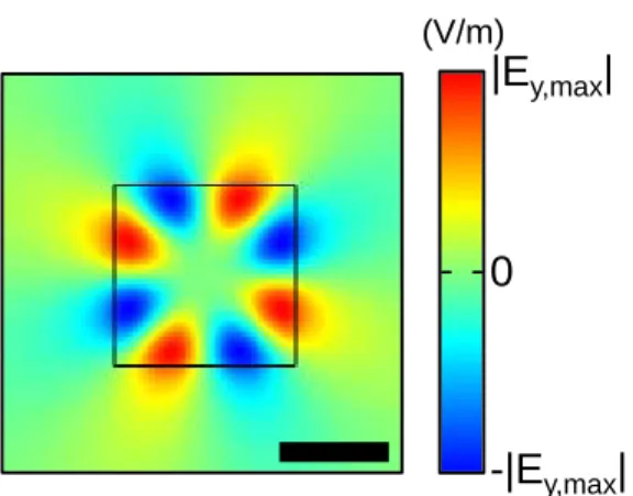
Many seminal works have been proposed in the context of active metasurfaces, using various active materials or mechanisms such as transparent conducting oxides [46-48], liquid crystal [55], phase-change materials [52], 2D materials electromechanical system and semiconductors [54]. Regarding the photonic structures, most of the reflective active metasurfaces exploit mirrors to achieve strong phase response at optical resonances. The electrical biases cause electrostatic forces between the neighboring rods, which lead to lateral movements of the nanostructures in the 𝑥 axis.
Theoretical and numerical study of asymmetric resonant metasurfaces 92
In general, the coupling condition between the gate and the resonator determines the phase response of the reflected light [183]. The metasurface has mirror symmetry in the 𝑧 direction with respect to the center of the nanostructure. The reflected power coefficient spectra for the positive phase gradient fired gratings are depicted in Fig.
Fabrication and optical characterization of the active metasurfaces
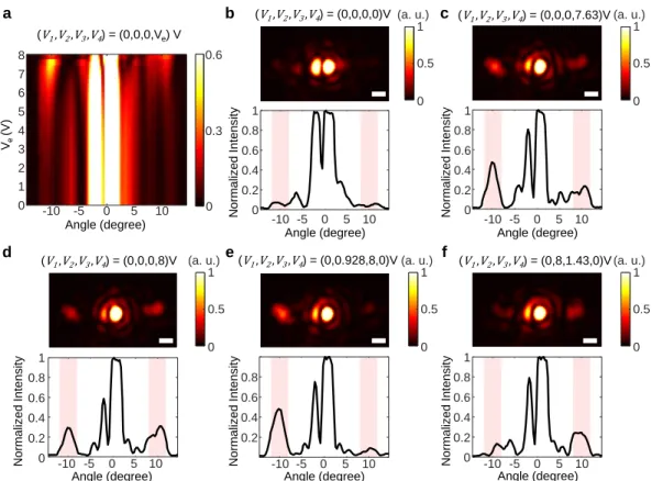
We believe that the deviation is due to the non-negligible bending of the nanostructures at the large applied bias. To measure the intensity as a function of applied bias, the reflectance is measured at 1524 nm with increasing applied bias from 0 to 8 V. Figure 5.4h shows the measured phase shifts as a function of applied bias at a wavelength of 1524 nm.
Experimental demonstration of electrically controllable diffraction
The intensity is measured at 1524 nm as a function of applied bias from 0V to 8V. At each bias, the intensity is normalized by the peak intensity near 0◦. To demonstrate efficient devices in the experiment, we create another set of metasurfaces with changes in electrical configuration (see Fig.5.A.9 for details). It shows experimentally that further optimization in the nanofabrication process improves the diffraction efficiency of the device.
Discussion and outlook
Although this intuitive approach allows large-scale design with moderate efficiency, the performance of metasurfaces can potentially be improved through an optimization process [205] . Specifically, parameterized adjoint optimization can be performed with arbitrary target wavefronts to determine the optimal distribution of distances between nanostructures [206] . At a moderate device size, we expect the parameterized adjoint optimization to yield a significant performance improvement.
Methods
Similar to the undercut process in [159], the time of the undercut process is carefully adjusted so that the anchors are supported by the SiO2 while the nanostructures are completely suspended. The custom printed circuit board can supply four independent voltages to the electrode sets in the device. Specifically, four different PWM (pulse width modulation) channels in Arduino are connected to four PWM to DC converter modules (LC-LM358-PWM2V) and a custom external circuit.
Appendix
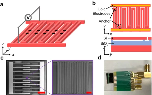
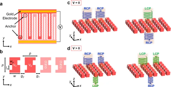
To characterize the chiroptical responses of the devices, the spectra 𝑅𝐿 , 𝐿 and 𝑅𝑅, 𝑅 are measured using the setup in Figure 6.A.1.
NEMS-tunable dielectric chiral metasurfaces
Introduction
In addition to devices operating in the THz or microwave domain, dynamic plasmonic chiral metasurfaces have also been extensively studied in the optical domain. Nevertheless, all the aforementioned tunable plasmonic chiral metasurfaces are inherently lossy, which limits the optical performance. In contrast to the extensive work on tunable plasmonic chiral metasurfaces, studies related to tunable dielectric chiral metasurfaces have been limited.
Main
Furthermore, 𝑅𝑅, 𝐿 and 𝑅𝐿 , 𝑅 are identical due to the symmetry of the unit cell [232] and this is confirmed by a gray curve plotted in Figure 6.2a. To simulate the mechanical tuning of the chiroptical effects, the spectra of 𝑅𝐿, 𝐿 and 𝑅𝑅, 𝑅 are calculated by varying the mechanical motion, 𝑔2−2𝑔1, from 0 to 80 nm and plotted in Figure 6.2c. To clearly visualize the change in chiroptical effects, |𝑅𝐿 , 𝐿−𝑅𝑅, 𝑅| evaluated based on Figure 6.2 and plotted in Figure 6.2d.
Discussion and Summary
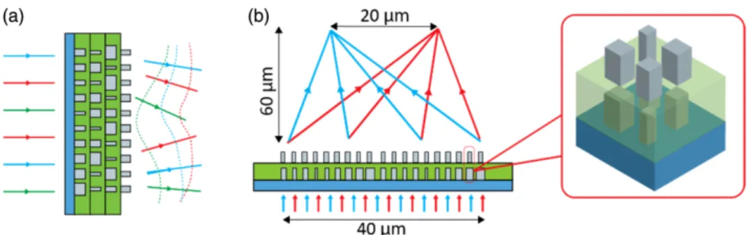
However, the design of the multilayer metasurface is a complicated task due to significant inter-layer coupling. To describe the overall design process of 2.5D metasurfaces, we use a double-layer metal lens shown in Fig. Also, the volume of the metasurface optical systems was on the order of 1-mm3 volume.
Methods
Appendix
Multilayer metastructures designed by adjoint optimization
Introduction
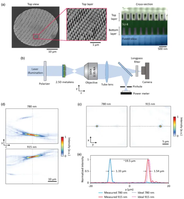
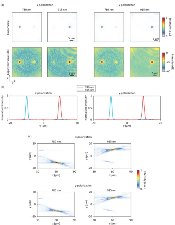
Multilayer metasurfaces offer a significantly larger number of degrees of freedom and can be used to implement multifunctional devices. Unlike most demonstrations to date that use a topological optimization scheme, we use parameterized meta-atoms that are more suitable for layer-by-layer fabrication. The simulated and experimentally measured focusing efficiency of the optimized device was found to be significantly higher than the simulated control efficiency, confirming the potential of the adjoint-based technique in the design of high-performance 2.5D multifunctional devices .
Design process and numerical investigations
The results of these simulations are used to calculate the gradient of the objective function with respect to the design parameters. In the coupled simulation shown in Fig.7.3b, the same structure is illuminated by coupled sources that are equal to the complex conjugate of the desired output fields. Figure 7.4a shows the evolution of the focusing efficiency of the device during the optimization process.
Experimental results
To confirm this, we performed further full-wave simulations of the optimized metalenes, but with an actual spacer thickness of 800 nm, resulting in efficiencies of 42% and 38%. The device described in this chapter was one of a large series of devices written with intentional displacements (up to 200 nm in both the 𝑥- and 𝑦-directions) in an effort to produce a device with minimal layer-to-layer misalignment. For reference, the mismatch between layers patterned by electron beam lithography is typically on the order of several tens of nanometers.
Discussion and conclusion
We experimentally characterized devices with a relative shift between layers to study this effect (see Fig.7.A.3 for the measured efficiencies with several different lateral shifts.). Although the fabrication process of 2.5D metastructures involves more steps than single-layer metasurfaces, the significant performance improvement is large enough to justify the more involved fabrication process. Multilayer structures with tens of nanometer tolerances are routinely fabricated in CMOS foundries, and similar processes can potentially be used to fabricate practical 2.5D multifunctional metastructures such as color separation filters for image sensors.
Methods
A linear polarizer (Thorlabs, LPVIS100-MP2) was placed in front of the collimator to confirm the polarization of the input light, and a fiber polarization controller was used to increase the power passing through the polarizer. An optical long-pass filter (Thorlabs, FEL0700) was placed in front of the camera to reduce background noise. The power incident on the device was measured by placing an iris in place of the pinhole and removing the sample and adjusting the diameter of the iris to actually be 40-𝜇m in diameter at the plane of the sample.
Appendix
Popescu, Quantitative phase imaging of cells and tissues (McGraw Hill Professional, 2011) (cit. on pp.7,53). Faraon, “Decoupling optical function and geometric shape using conformal flexible dielectric metasurfaces,” Nature communications cit. on page 41). Zhang et al., “Photo-induced handedness switching in terahertz chiral metamolecules,” Nature communications cit. on page 119).
Conclusion and outlook
Summary and Contributions
Outlook
Wu et al., “Dynamic beam steering with multiple electro-optical iii–v all-dielectric quantum well metasurfaces,” Nature communications cit. on pp. 5, 91). Lee et al., “An endoscope with integrated transparent bioelectronics and theranostic nanoparticles for the treatment of colon cancer,” Nature communications cit. on p. 53). Smalley et al., "Pixelated subwavelength cmos color sensors based on antihermitian metasurface," Nature communications cit. on pg. 148).
Simulations on nano-electromechanical phase modulation and beam
Optical characterization of dynamic properties of the asymmetric
Tunable diffraction with the asymmetric nano-electromechanical meta-
Dielectric chiral metasurfaces and measurements of chiroptical rep-
Multifunctional 2.5D metastructure
Direct and optimized design methods of 2.5D metastructures