Output and transmission characteristics of the ambipolar device fabricated with PMMA/PVA as the dielectric material measured under vacuum conditions. Dual sweep transmission characteristics of the ambipolar device fabricated with PMMA/PVA as the dielectric material measured under vacuum conditions.
Abstract
As in the case of PDI polymers, annealing of thin films of these polymers also results in improved intermolecular interactions in the thin-film state at the macroscale, facilitating enhanced and higher charge carrier transport in annealing devices. compared to spin devices which have smaller crystalline phases. Extended conjugation in the copolymer structures, efficient intermolecular interactions in the thin-film state, and the formation of crystalline domains in the copolymers after annealing improved the device performance.
It was observed that as the channel length decreases, the IDS increases and the HMDS layer increases the ion/Ioff ratio of the device.
Bare substrate with Al foil Gate Final device
Contents
Synthesis of Perylenediimide based polymers and fabrication of Organic Field Effect Transistors
Chapter 3: Synthesis of Naphthalenediimide based polymers and fabrication of Organic Field Effect Transistors
Effect of dielectric material, SAM and channel length on the performance of the Perylenediimide based OFETs
Introduction
- Organic Semiconductors
- Organic electronic devices
- Organic field-effect transistors
- Fabrication of Organic field-effect transistors
- Working principle of Organic field-effect transistors
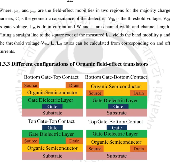
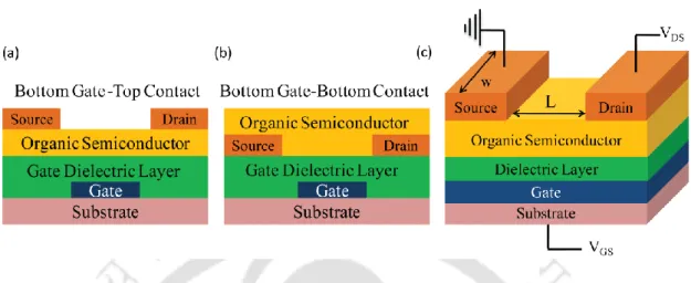
- Different configurations of Organic field-effect transistors
- Types of Organic Semiconductors
- p-type Semiconductors
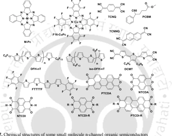
- n-type Semiconductors
- Ambipolar Semiconductors
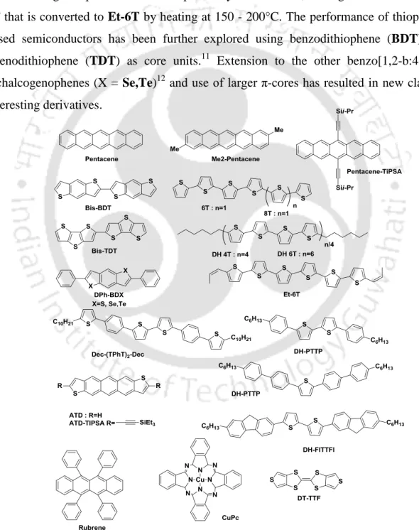
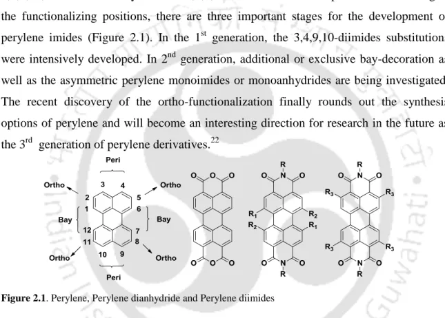
- Rylenediimide based n-type semiconductors
- Perylenediimide based Small molecules
- Perylenediimide based Polymers
- Naphthalenediimide based Small molecules
- Naphthalenediimide based Polymers
- Different types of Substrates
- Role of the Gate dielectric
- Modification of dielectric by Surface assembled monolayers
- Contact Resistance and channel length
- Stability of the OFETs
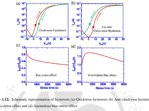
- Hysteresis
- Bias-stress effect
- References
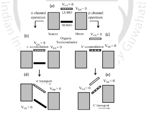
The contact condition of the electrode/organic interface also depends on the geometry of the device. Some mechanisms causing hysteresis in OFETs are already quite well described in the literature.
Synthesis of Perylenediimide based
- Introduction
- Experimental Section
- Materials and Instruments
- Preparation of films for AFM, FESEM, XRD and POM
- Synthesis of Monomers and Polymers
- Device fabrication and characterization
- Results and discussion 1. Characterizations
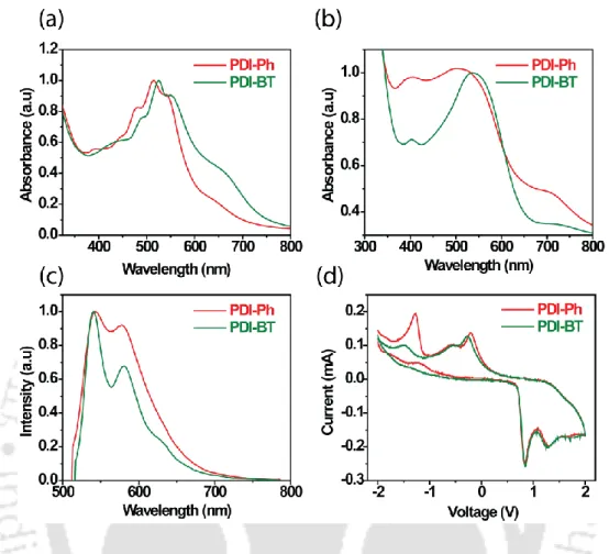
- Photophysical Properties
- Electrochemical Properties
- Thermal Properties
- Morphology Characterization
- OFET Measurements
- Conclusions
- References
The solution was concentrated to 5 mL and added dropwise to 50 mL of methanol. The precipitate was filtered and washed twice with methanol to give a black colored solid. The surface of the dielectric was coated (1500 revolutions per minute for 30 s) with a thin monolayer of hexamethyldisilazane (HMDS) and annealed for 2 hours at 110 °C. The HOMO and LUMO energy levels of the copolymers were evaluated using a cyclic voltammetry (CV) experiment.
The thermal properties of the polymers were investigated by thermogravimetric analysis (TGA) and differential scanning calorimeter (DSC).
Synthesis of Naphthalenediimide
- Introduction
- Experimental Section
- Materials and Instruments
- Preparation of films for AFM, FESEM, XRD and POM
- Synthesis of Monomers and Polymers
- Device fabrication and characterization
- Results and discussion 1. Characterizations
- Photophysical Properties
- Electrochemical Properties
- Thermal Properties
- Morphology Characterization
- OFET Measurements
- Conclusions
- References
Detailed transport investigation of the NDI copolymers was performed using bottom gate, top contact FET geometry. High OFET can be attributed to the enhanced π-π stacking arising from the intermolecular overlap of the DA orbitals. The absorption spectra of the spin-coated polymer films on glass (Figure 3.2(b)) showed red shift in the peaks for all copolymers compared to the absorption peaks in the solution state.
Out-of-plane XRD measurements were performed on thin films of the NDI copolymers (Figure 3.4, 3.5) to obtain information about the molecular reorganization.
Effect of dielectric material, HMDS and channel length on the
Introduction
In OFETs, the energy mismatch between Fermi level of metal contact and HOMO or LUMO level of the organic semiconductor and morphology of the semiconductor determine the contact resistance value. This includes gate modulation of the bulk resistance of the semiconductor to explain the experimentally observed gate voltage dependence of the contact resistance for different thicknesses of the semiconductor film. Therefore, it will be possible to inject three times larger amount of carriers into the organic layer on PVA than on PMMA if the thickness of the dielectric is the same, and the best dielectric breakdown properties are actually achieved.
In this chapter, the fabrication process and device performance with the variation in channel length and the surface modification of the dielectric layer were demonstrated.
Experimental section
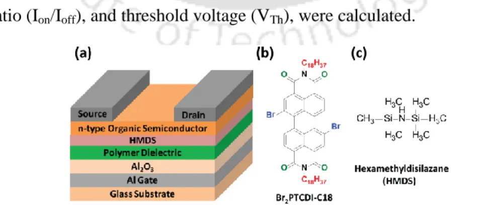
- Synthesis of Br 2 PTCDI-C18
- Fabrication of OFET
Effect of Dielectric Material, HMDS and Channel Length on the Performance of Perylene Diimide Based OFETs. Another set of PVA or PMMA substrates was coated with HMDS to study the effect on top layer growth and device performance. Synthesized and purified Br2PTCDI-C18 was chosen as the n-type organic semiconductor and thermally evaporated on top of the double-layer dielectric system of approximately 50 nm.
Effect of dielectric material, HMDS and channel length on the performance of perylenediimide-based OFETs.
Results and Discussion
- Morphological studies of different dielectric layers
- Devices fabricated with Al 2 O 3 /PVA as dielectric
- Devices fabricated with Al 2 O 3 /PVA/HMDS as dielectric
- Devices fabricated with Al 2 O 3 /PMMA as dielectric
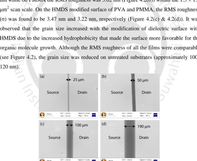
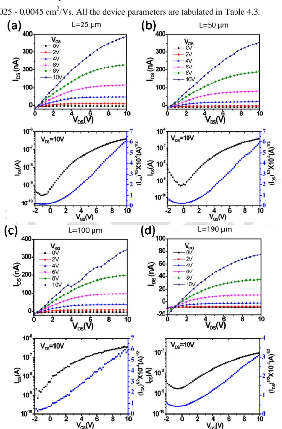
The surface morphology of the Br2PTCDI-C18 films on different substrates was characterized using AFM (Figure 4.2). Although the RMS roughness of all the films was comparable (see Figure 4.2), the grain size was reduced on untreated substrates (approximately 100-120 nm). The OFETs using Al2O3/PVA gate dielectrics showed mobility in the range cm2/Vs for the different channel lengths.
Summary of electrical parameters of organic field effect transistors based on Al2O3/PVA dielectric and organic semiconductor Br2PTCDI-C18, fabricated with different channel lengths measured under vacuum conditions inside the probe station.
O 3 /PVA/Br 2 PTCDI-C18
The OFETs using Al2O3/PVA/HMDS gate dielectrics showed high performance and mobility in the range of cm2/Vs for the different channel lengths. Output and transfer characteristics of the OFET device fabricated on Al2O3/PVA/HMDS as the dielectric material with different channel lengths (a) L= 25 μm (b) L= 50 μm (c) L=100 μm (d) L=190 μm . Summary of the electrical parameters of the Al2O3/PVA/HMDS dielectric and Br2PTCDI-C18 organic semiconductor-based organic field-effect transistors fabricated with different channel lengths measured under vacuum conditions in the probe station.
Summary of electrical parameters of organic field effect transistors based on Al2O3/PMMA dielectric and organic semiconductor Br2-PTCDI-C18, fabricated with different channel lengths measured under vacuum conditions inside the probe station.
O 3 /PVA/HMDS/Br 2 PTCDI-C18
O 3 /PMMA/ Br 2 PTCDI-C18
- Devices fabricated with Al 2 O 3 /PMMA/HMDS as dielectric
- Variation of I DS and Contact resistance with Channel length
It can be observed that the drain current (IDS) increased compared to the devices based on the PMMA dielectric layer, but the threshold voltages and other properties were also improved. Summary of electrical parameters of organic field effect transistors based on Al2O3/PMMA/HMDS dielectric and organic semiconductor Br2PTCDI-C18 fabricated with different channel lengths measured under vacuum conditions inside the probe station. The contact resistances are derived using the linear fit of these curves with the TLM (Transmission Line Method) and are shown in Table 4.5.
The contact resistance depends on the morphology of the organic semiconductor, nature of the dielectric material, grain size and density of the grain boundaries at the source/drain electrode.
O 3 /PMMA/HMDS/ Br 2 PTCDI-C18
- Bias Stress measurements
- Conclusions
- References
- Introduction
- Experimental section
- Synthesis of Br 2 PTCDI-C18
- Fabrication of ambipolar OFET devices
- Results and discussions
- Leakage current and capacitance measurements
- Morphology of different layers in the flexible OFET device
- Device Characterization under vacuum conditions 1. Transfer and Output Characteristics
Output and transfer characteristics of the OFET device fabricated on Al2O3/PMMA/HMDS as the dielectric material with different channel lengths (a) L= 25 μm (b) L= 50 μm (c) L=100 μm (d) L= 190 µm. Images of the laminated Al foil on pristine OHP sheet and the final devices are shown in Figure 5.1(d). Output characteristics of the ambipolar device fabricated using PMMA/PVA as the dielectric material (a) n-type (b) p-type.
Transmission characteristics of an ambipolar device fabricated using PMMA/PVA as dielectric material (c) n-type (d) p-type measured under vacuum conditions.
Dual Sweep Characteristics of PMMA/PVA device
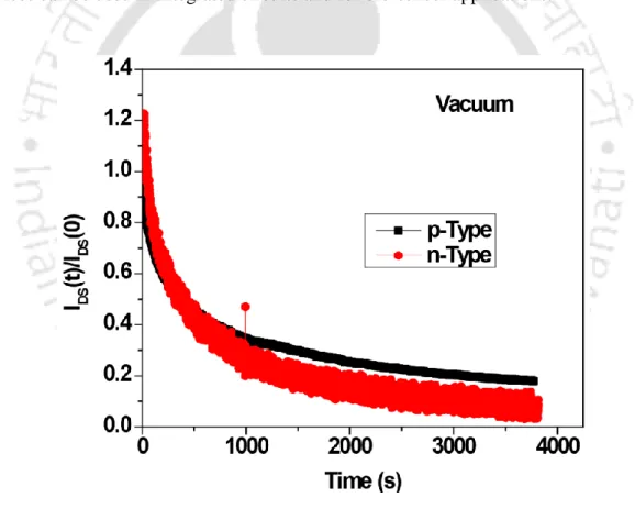
Clockwise hysteresis is due to the charge traps at the dielectric and semiconductor interface, where as in this case it can be due to the slow polarization of polar dipoles in the dielectric materials with the applied gate voltage under vacuum conditions. A threshold shift was observed in the n-type behavior, while it was negligible in the p-type. More the shift in n-type transfer characteristic curve indicates that more electrons are trapped in the channel in the n-type measurement than the holes in the p-type measurements.
The measured threshold voltage shift values for the n-type and p-type transports of the OFETs are 3 V and 0.5 V.
Back to back scan measurements of PMMA/PVA device
Device Characterization under humidity conditions
In the presence of water molecules, the polarization of the dipoles becomes faster and induces more charges at the interfaces, leading to a decrease in charge trapping and an increase in drain current. This may be a consequence of the complete polarization of polar dielectric dipoles (–OH group) in the presence of water molecules from ambient conditions.32 However, in a vacuum, dipole polarization takes place slowly and the number of charges induced in the interface is low. Balanced ambipolar behavior of OFET device fabricated using PMMA/PVA as dielectric material measured under humidity conditions.
Summary of the electrical parameters of the PMMA/PVA dielectric based organic field effect transistor measured under humidity conditions.
Bias stability of PMMA/PVA based OFET under vacuum and ambient conditions
In electron transport, the current initially increased and starts to decay to 50% of the initial value at the end of the 1 hour measurement time. In general, the current decay under bias is due to charge retention at the interface and in the semiconductor/dielectric material. On the other hand, at the anomalous bias, the current enhancement with bias time is due to the slow polarization of the dipoles in the polar dielectric material.
For electron transport, the current immediately decayed to 40% and remained almost constant for the rest of the measurement time.
Ambipolar OFET fabrication and characterization using the cross linked PVA
Although both curves decreased with time, the overall decrease is 45% in p-type transport and 60% in n-type transport for 1 hour of bias measurement under ambient conditions. For n-type transport under ambient conditions, the rapid decay occurring immediately after the device was turned on suggested that the charge traps at the dielectric semiconductor/gate interface predominantly and rapidly interacted with the available mobile carriers in the channel region. Typical output characteristics of the ambipolar OFET in hole gain mode and electron gain mode operations are shown in Figures 5.9(a) and 5.9(b).
Summary of the electrical parameters of the C-PVA dielectric based organic field effect transistor measured under vacuum conditions.
- C-PVA device bias stability under vacuum and humidity conditions
- Long term Stability of PMMA/PVA based ambipolar OFET
- Conclusion
- References
Transfer characteristics of the ambipolar device fabricated using PMMA/PVA as the dielectric material for n-type and p-type behavior measured after 8 months under vacuum conditions. Long-term device stability is a crucial factor for the practical application of the OFET devices. The performance and dual polarity of the ambipolar devices were systematically studied under vacuum and humidity conditions.
All the electrical, ambient and long-term stabilities of the devices were systematically investigated and presented here.
Conclusions
These copolymers showed an increase in electron mobility by several orders of magnitude, reported to be up to 0.8 cm2 V/s and 0.2 cm2 V/s for NDI-PH and NDI-BT, respectively, with Ion/Ioff ratios of 103-104. Devices were fabricated with channel lengths of 25 µm, 50 µm, 100 µm, 190 µm with all combinations of different dielectric systems Al2O3/PVA, Al2O3/PMMA, Al2O3/PVA/HMDS, Al2O3/PMMA/HMDS. In the first device, PMMA/PVA was used as a dielectric layer and achieved electron and hole mobilities of up to 1.2×10⁻² cm2 V/s and 5.5×10⁻³ cm2 V/s, respectively, at operating voltages of ± 10V.
Then, in the second device, we used C-PVA (Crosslinked PVA) as a dielectric material and the operating voltages were further reduced to ± 3V.
List of Publications
Conferences