They are based on the generation of electron-hole pairs in the depletion region of the junction being formed. This involves precise control of doping concentrations in the active region and the guard ring regions of the device.
![Figure 1.1 Hybrid Photo Detector [3]](https://thumb-ap.123doks.com/thumbv2/azpdfnet/10509012.0/16.918.326.597.306.531/figure-1-1-hybrid-photo-detector-3.webp)
Structural and Device Simulation
- Schokley-Read-Hall (SRH) Recombination
- Auger Recombination and Generation
- Mobility Models
- Band Structure
- Avalanche Generation
- Okuto-Crowell Model
- Lackner Model
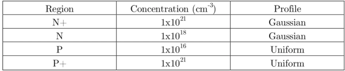
The parameters used in the Structural definition of the device are as in Table 3.1 Table 3.1: Dimensions of different regions of proposed structure. The diode contains regions of different concentrations, mobility of the electrons and holes depends on the doping concentration at the point of interest in the device. The built-in electric field of the device depends on the doping profile which in turn affects the mobility.
It is known that the mobility of electrons and holes depends on the average collision time of the carriers. This effect must therefore be considered as it affects most of the physical phenomenon in a semiconductor device, including the effective intrinsic concentrations of electrons and holes in the device.
Wafer Specification
RCA Cleaning
RCA I
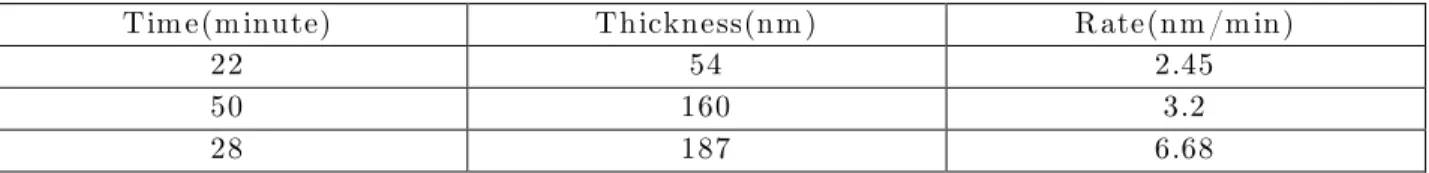
Hydrogen (H2) and oxygen (O2) gas are introduced at flow rates of 70 and 100 lpm respectively. 4 •The process runs for 56 minutes. This creates fall points that can be attributed to the high ideality factor of the devices. The presence of protective rings and the uniform electric field it introduces into the device can be attributed to these features of the devices.
The obtained CV characteristics of the diode are thus in line with the ideal characteristics of the diode. The gain characteristics also show high bombardment gain with increasing electron acceleration.
RCA II
Thermal Oxidation
This type of oxide is used when the oxide plays a very important role in determining the properties of the device such as MOSFET. In wet oxidation, the oxide layer is formed by the reaction of silicon with water vapors passing through. This type of oxide is generally preferred for use when the oxide layer is used as a sacrificial layer.
For the production of the proposed device, the oxide is used as a mask for the ion diffusion and implantation process. Thus, we have to go into wet oxidation to get the desired thickness of the oxide layer.
Lithography
Silicon Dioxide etching
Silicon Etching
Resist Removal
Piranha Cleaning
Diffusion
Ion Implantation
- Carrier Gas pressure
- RF Power
- Substrate Bias
- Implantation Duration
- Pulse on Duration
- Frequency of Substrate bias
- Distance between plasma and substrate
- Gas Flow
The substrate bias is an important parameter in determining the junction depth of the implanted sample. The higher the substrate bias, the deeper the ion acceleration will be the implantation thus increasing the coupling depth of the device. When the substrate bias is applied, the ion envelope expands and ions enter the substrate.
The substrate bias frequency determines how many times the ion envelope expands, thereby implanting ions into the substrate. The higher the frequency, the greater the envelope expansion, thereby increasing the dose of implanted ions to the substrate.
Inductively Coupled Plasma Chemical Vapour Deposition (ICPCVD) for Oxide
This is also accompanied by higher etching as more exposure to the ions is experienced. If the distance between the substrate and the plasma is smaller, as the sheath expands, the sheath may touch the plasma source, affecting the ions penetrating the substrate. Thus, as the distance increases, the sheath expands, increasing the velocity and thus increasing the depth of penetration.
Thus, the greater the distance between the plasma source and the substrate, the greater the penetration depth.
Rapid Thermal Processing (RTP)
Metal Deposition using 4 Target E Beam Thermal evaporator
Metal deposition using Thermal evaporator (Al)
Lift Off
Annealing for alloying
Characterization
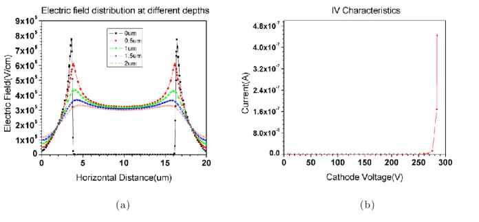
From the distribution of the electric field obtained for different models it is clear that with the use of protective rings a uniform electric field is obtained throughout the active area of the device compared to devices without protective rings. With the different steps mentioned in the previous chapter, avalanche diodes with and without protective rings were fabricated. The leakage current obtained is also less when compared to devices without protective rings.
From the gain characteristics obtained in the devices without guard rings, it was clear that a lower leakage current would be the avalanche gain. Since it has been shown from the obtained characteristics that devices with protective rings contribute less leakage current, we can conclude that devices with protective rings also improve the avalanche amplification of the device.
TCAD Simulation results
Electric Field distribution, IV characteristics and breakdown voltage for
- Electric field distribution and IV Characteristics for Silicon
- Electric field distribution and IV Characteristics for Silicon
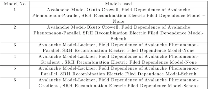
SRH recombination generation model with doping and temperature dependence, Auger recombination generation model, band tunneling model, mobility with doping dependence and electric field model were used in all simulations for devices with and without guard rings with variations in avalanche breakdown models. 1 Avalanche M odel-Okuto Crowell, Field Dependence of Avalanche Phenomenon-Parallel, SR H R ecom bination Electric Filed D dependence M model. 2 Avalanche M odel-Okuto Crowell, Field Dependence of Avalanche Phenomenon-Parallel, SR H R ecom bination Electric Filed D dependence M model-.
3 Avalanche M odel-Lackner, Field Dependence of Avalanche Phenom enon - Parallel, SR H R ecom bination Electric Filed Dependence M odel-N one 4 Avalanche M odel-Lackner, Field D ependence of Avalanche Phenom enon. G radient , SR H Recom bination Electric Filed Dependence M odel-N one 5 Avalanche M odel-Lackner, Field Dependence of Avalanche Phenom enon - Parallel, SR H R ecom bination Electric Filed Dependence M odel-Schenk 6 Avalanche M odel- Lackner, Field Dependence of Avalanche Phenom enon - G radient , SR H Recom bination Electric Filed Dependence M odel-Schenk.
Fabrication results
Resistivity to doping concentration conversions
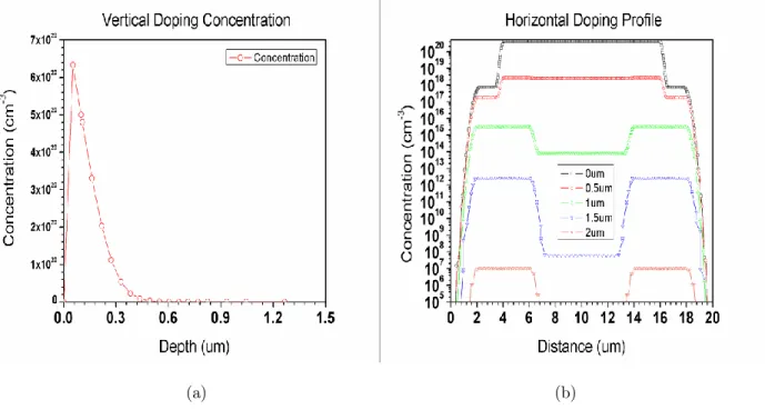
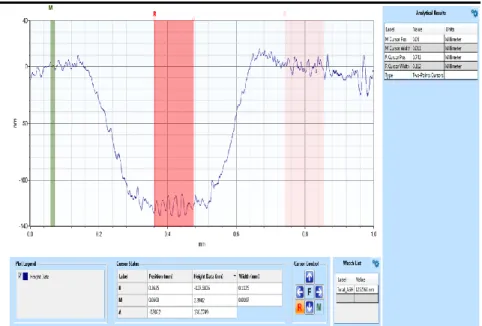
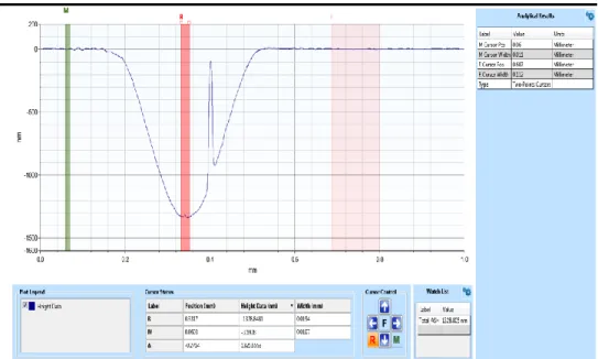
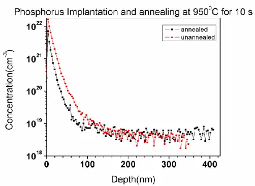
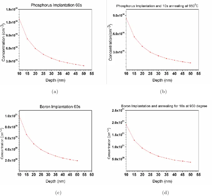
Where 𝜌 is the resistivity, n and p represent the concentration of electrons and holes, respectively, un and up represent the mobility of electrons and holes, respectively, and e is the electric charge. The conversion from resistivity to concentration generally gives the concentration of the majority carrier in the doped sample. From Fig. 5.14 and 5.15 we obtain an approximate profile for the implanted samples, which can be used for calculations in the absence of advanced analytical instruments.
FESEM Images of the Fabricated Devices
Electrical Characterization of the fabricated devices
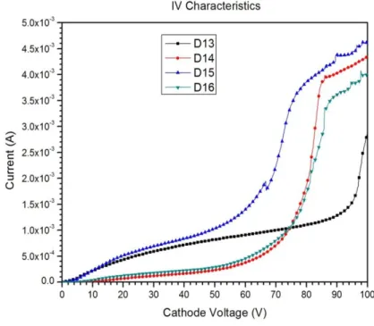
Since the target devices are those with guard rings more devices were characterized and the device characteristics obtained are shown below. From the parameters in Tables 5.4, 5.5 and 5.6 it is evident that the leakage current is mostly less in the protective ring device and shows a better ideality factor. Thus, devices with guard rings would naturally have higher gain around the breakdown voltage if used compared to those without them.
Thus, the use of devices with guard rings can generally be used in applications that require very high sensitivity, and due to the increased breakdown voltage shown in the characteristics, it can also be used in applications that require higher stability. Few devices with guard rings were obtained with breakdown characteristics were obtained for voltages less than 100V, but the breakdown voltages obtained were higher than for devices without guard rings.
Bombardment Gain
The 1/C2 characteristics showing non-uniform symmetry indicate non-uniform doping around the junctions, which is as expected from the SIMS profile obtained for doping. The fabricated devices have spherical symmetry, so the surface area of the metal pads was equated to that of a circle to determine the radius. The effective area was calculated using the radius obtained and the depletion width corresponding to different voltages was calculated using the capacitance obtained for the applied voltages using the model of a parallel plate capacitor. The results obtained are as shown in Figure 5.34.
Bombardment gain is given by the energy of the electron on the silicon surface at 3.6ev (Energy required to create an electron-hole pair).
Gain of the Hybrid Photo detector
In this work, the Si Avalanche Diodes with Guard rings were successfully fabricated using a CMOS compatible process as an electron bombardment substrate and as an avalanche electron multiplier in hybrid photodiode applications. The simulated results also show that the uniform electric field is obtained through the use of guard rings, which basically avoids the premature breakdown of the devices, which was verified by the inverse characteristics of the fabricated devices where the devices without guard rings prematurely showed signs of failure compared to the devices with guard rings. The IV characteristics also show that the devices with guard rings behave better near the ideal diodes, which can be verified by the ideality factor and leakage current calculations.
The leakage current in devices with protective rings is smaller due to a uniform electric field in the entire active area of the device, since a higher electric current in some parts of the device can trigger an unwanted current in the off state, so the use of protective rings reduces the leakage current in this part is also presented. It can be concluded that the combination of high electron acceleration from the photocathode leads to a high gain when bombarded on a silicon substrate with a further enhancement of the gain achieved by using an avalanche diode with guard rings to obtain a gain in the range of 2.5x10⁸, leading to the use of the proposed hybrid photodetector in very sensitive applications.
Future Work
Thus, the photocathode and silicon avalanche diode must be housed in a high vacuum chamber with the outer casing magnetically and electrically inactive so that no external photons enter the system other than from the actual entrance to the system and no change occurs. in the electron path as it moves from the photocathode to the silicon avalanche diode. If all the above conditions are met, it is necessary to measure the number of charges generated by the impact of a photon on the detector and calibrate the response time of the sensor. The design of a high-sensitivity readout circuit to be integrated into the detector must also be done as part of the entire hybrid photodetector design flow.
DE MAN, "Measurement of the Ionization Rates in Diffused Silicon p-n Junctions", Solid-State Electronics, Pergamon Press 1970. 28] Ashok Kumar Ray,"Plasma Immersion Ion Implantation Process Space Optimization for Semiconductor Device Applications", A thesis submitted in partial fulfillment of the requirements for the degree of Master of Technology IIT Bombay, June SHU QIN, James D Bernstein and Chung Chan, "Hydrogen etching for semiconductors.
![Figure 2.4: a) Avalanche Diode without Guard ring b) Avalanche diode with guard ring [4]](https://thumb-ap.123doks.com/thumbv2/azpdfnet/10509012.0/22.918.139.841.569.844/figure-avalanche-diode-guard-ring-avalanche-diode-guard.webp)