저작자표시-비영리-변경금지 2.0 대한민국 이용자는 아래의 조건을 따르는 경우에 한하여 자유롭게
l 이 저작물을 복제, 배포, 전송, 전시, 공연 및 방송할 수 있습니다. 다음과 같은 조건을 따라야 합니다:
l 귀하는, 이 저작물의 재이용이나 배포의 경우, 이 저작물에 적용된 이용허락조건 을 명확하게 나타내어야 합니다.
l 저작권자로부터 별도의 허가를 받으면 이러한 조건들은 적용되지 않습니다.
저작권법에 따른 이용자의 권리는 위의 내용에 의하여 영향을 받지 않습니다. 이것은 이용허락규약(Legal Code)을 이해하기 쉽게 요약한 것입니다.
Disclaimer
저작자표시. 귀하는 원저작자를 표시하여야 합니다.
비영리. 귀하는 이 저작물을 영리 목적으로 이용할 수 없습니다.
변경금지. 귀하는 이 저작물을 개작, 변형 또는 가공할 수 없습니다.
P
H.D. D
ISSERTATION12-C HANNEL T RANSMITTER WITH D ATA - D EPENDENT J ITTER C OMPENSATION U SING
P HASE AND A MPLITUDE E MPHASIS T ECHNIQUE
위상 및 진폭 강조 기술을 사용하여 데이터 종속 지터 보상 기능을 가지는 12 채널 송신기
BY
J
IHWANP
ARKF
EBRUARY2018
D
EPARTMENT OFE
LECTRICALE
NGINEERING ANDC
OMPUTERS
CIENCEC
OLLEGE OFE
NGINEERINGS
EOULN
ATIONALU
NIVERSITY12-C HANNEL T RANSMITTER WITH D ATA -D EPENDENT J ITTER C OMPENSATION U SING P HASE AND A MPLITUDE E MPHASIS
T ECHNIQUE
위상 및 진폭 강조 기술을 사용하여 데이터 종속
지터 보상 기능을 가지는 12 채널 송신기
지도교수 김 수 환
이 논문을 공학박사 학위논문으로 제출함 2018 년 2 월
서울대학교 대학원 전기컴퓨터 공학부
박 지 환
박지환의 공학박사 학위논문을 인준함 2018 년 2 월
위 원 장 : 정 덕 균 ( 印 )
부위원장 : 김 수 환 ( 印 )
위 원 : 이 혁 재 (印)
위 원 : 전 동 석 ( 印 )
위 원 : 전 정 훈 ( 印 )
A BSTRACT
12-C HANNEL T RANSMITTER WITH D ATA - D EPENDENT J ITTER C OMPENSATION U SING
P HASE AND A MPLITUDE E MPHASIS T ECHNIQUE
J
IHWANP
ARKD
EPARTMENT OFE
LECTRICALE
NGINEERING ANDC
OMPUTERS
CIENCEC
OLLEGE OFE
NGINEERINGS
EOULN
ATIONALU
NIVERSITYIn this thesis, a 2.1Gbps 12-channel transmitter using phase emphasis for UHD intra- panel interface is presented. High-speed data must be transmitted from timing controller (TCON) to multiple source drivers (SD) to support high resolution in UHD intra-panel interface. To optimize output signal according to various channel conditions between TCON and SD, each channel driver is designed to control common mode voltage, swing level, and emphasis level of output signal by using PVT insensitive current. Also, the amplitude emphasis and phase emphasis technique are applied to the transmitter to compensate for worst channel with a loss of more than 10dB in the intra-pane interface.
The phase emphasis compensates data-dependent-jitter (DDJ) due to the limited bandwidth of the channel by varying the transition start timing according to the data
I
sequence. Therefore, a certain amount of channel loss can be compensated by phase emphasis, which reduces burden on signaling for amplitude emphasis. This paper includes not only the circuit implementation of the phase emphasis scheme but also the mathematical analysis, thus suggesting a method to design and modify the transmitter according to the channel environment to be used.
This transmitter is fabricated in 28nm COMS process and its area is 1.35mm2. For a 2.1Gbps PRBS of 27-1 passing through a 10dB loss PCB trace, the measured eye jitter is reduced by 38% by applying the emphasis, and the decrease amount by the phase emphasis reached 50% of the total decrease amount. The proposed transmitter is verified with 55-inch UHD (3840x2160) resolution TFT-LCD intra-panel interface. Our transmitter consumes 12.73mW/Gb/s per channel with 1.2V of output swing level.
Keywords: timing controller (TCON), source driver (SD), data-dependent-jitter (DDJ), phase emphasis, UHD, intra-panel interface
Student Number: 2012-30209
II
C ONTENTS
ABSTRACT ... I
CONTENTS ... III
LIST OF FIGURES ...V
LIST OF TABLES ... IIX
CHAPTER 1 INTRODUCTION ... 1
1.1 MOTIVATION ... 1
1.2 THESIS ORGANIZATION ... 6
CHAPTER 2 INTRODUCTION TO TFT-LCDINTRA-PANEL INTERFACE ... 7
2.1 BUS TOPOLOGY OF INTRA-PANEL INTERFACE ... 7
2.2 SIGNALING AND TERMINATION SCHEME ... 10
2.3 EQUALIZATION SCHEME ... 15
CHAPTER 3 PHASE EMPHASIS ... 22
3.1 DATA DEPENDENT JITTER (DDJ) ... 22
3.2 THE CONCEPT OF PHASE EMPHASIS ... 25
3.3 ANALYSIS OF DDJ AND PHASE EMPHASIS FOR DDJCOMPENSATION ... 31
CHAPTER4 INTRA-PANEL INTERFACE TRANSMITTER ... 47
4.1 INTRA-PANEL INTERFACE TRANSMITTER ARCHITECTURE ... 47
III
4.2 CLOCK GENERATION UNIT ... 50
4.3 LVDSDRIVER WITH HIGH TUNABILITY ... 53
4.4 20:1SERIALIZER WITH PHASE EMPHASIS TECHNIQUE... 56
CHAPTER5 EXPERIMENTAL RESULTS ... 71
5.1 EXPERIMENTAL SETUP ... 71
5.2 PLLJITTER PERFORMANCE AND SSCGPROFILE ... 78
5.3 EYE DIAGRAMS WITH DIFFERENT EMPHASIS SETTINGS ... 81
5.4 TCONMEASUREMENT RESULTS ... 85
CHAPTER6 CONCLUSIONS ... 88
BIBLIOGRAPHY ... 90
IV
L IST OF F IGURES
Fig. 1.1.1. Comparison of common TV resolutions (SD, HD, FHD, UHD) ... 2
Fig. 1.1.2. Trend of demand forecast for flat panel TV market ... 2
Fig. 1.1.3. (a) The intra-panel interface configuration, (b) the insertion loss (S13) of worst/best channel, and (c) the worst/best channel structure of UHD LCD module for large-sized TV application. ... 3
Fig. 2.1.1. The architecture of multi-drop topology ... 8
Fig. 2.1.2. The architecture of PPDS point-to-point topology ... 9
Fig. 2.1.3. The architecture of clock embedding topology ... 9
Fig. 2.2.1. Channel configuration for eye mask specification with source driver IC ... 11
Fig. 2.2.2. Voltage mode driver of high speed link interface ... 11
Fig. 2.2.3. Current mode driver of high speed link interface... 12
Fig. 2.2.4. Push-pull current mode driver of high speed link interface ... 13
Fig. 2.3.1. Equalization scheme for high speed interface ... 15
Fig. 2.3.2. Mode conversion problem due to unbalanced signaling ... 17
Fig. 2.3.3. Cherry-hooper type continuous time linear equalizer (CTLE)... 18
Fig. 2.3.4. High frequency noise boosting issue in linear equalizer at receiver ... 19
Fig. 2.3.5. Decision feedback equalizer (DFE) z-domain model. ... 20
Fig. 3.1.1. Eye diagram and jitter histogram at receiver front-end without equalization .. 23
Fig. 3.2.1. Eye diagram and jitter histogram with phase emphasis technique ... 25
Fig. 3.2.2. Phase emphasis implementation method and transition signal table... 27
Fig. 3.2.3. Phase emphasis scheme at the driver with quadrature rate operation ... 29
Fig. 3.2.4. Block diagram for pre-emphasis driver with phase emphasis ... 30
Fig. 3.3.1. Response of a general LTI system for a single bit response ... 31 Fig. 3.3.2. A description of the changes in two single bit responses with different width by
V
phase emphasis ... 33
Fig. 3.3.3. A clock pattern response with LTI system ... 34
Fig. 3.3.4. A description of the changes in clock pattern response and single bit response by phase emphasis ... 34
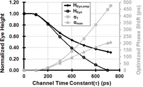
Fig. 3.3.5. The calculated normalized eye height and optimized phase shift versus channel time constant ... 37
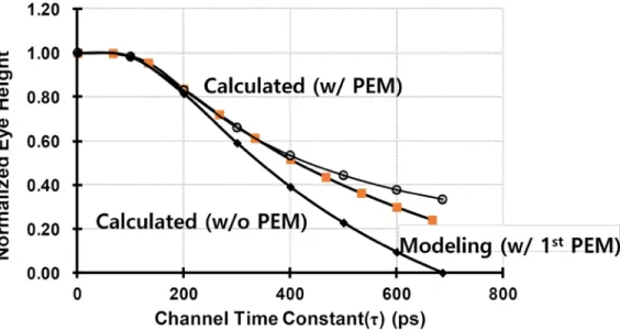
Fig. 3.3.6. The comparison between calculated result and modeling result of normalized eye height ... 38
Fig. 3.3.7. Total phase shift and 1st tap phase shift coefficient versus channel time constant ... 39
Fig. 3.3.8. Single bit impulse and output waveform with amplitude emphasis ... 40
Fig. 3.3.9. The whole summation of phase shift versus channel time constant with different amplitude emphasis level ... 42
Fig. 3.3.10. The normalized DDJ compensation ratio by phase emphasis versus channel time constant with different amplitude emphasis level ... 42
Fig. 3.3.11. The process to find out phase shift coefficient of real channel ... 44
Fig. 3.3.12. The measured and extracted channel frequency characteristics ... 46
Fig. 3.3.13. The compensated eye width versus 1st-tap phase emphasis coefficients for multi-pole channel ... 46
Fig. 4.1.1. The architecture of the proposed 12-channel transmitter ... 48
Fig. 4.2.1. PLL block diagram and specification in UHD intra-panel interface ... 50
Fig. 4.2.2. Overall duty-cycle corrector(DCC) structure and the schematic of DCC cell . 52 Fig. 4.2.3. Inverter based buffer with ac coupling capacitor for DCC ... 52
Fig. 4.3.1. PVT insensitive driver with wide common mode and voltage swing level controllability ... 54
Fig. 4.3.2. The schematic of band gap reference (BGR) ... 55
Fig. 4.4.1. 20:1 serializer with skew matched clock buffering ... 56
Fig. 4.4.2. 5:1 serializer and its timing diagram ... 57
Fig. 4.4.3. Five-latch 2:1 serializer and its timing diagram ... 57
VI
Fig. 4.4.4. The proposed 2:1 serializer with phase emphasis technique ... 58
Fig. 4.4.5. The full-rate based transition detect block with loading issue ... 60
Fig. 4.4.6. The full-rate modified transition detect block ... 61
Fig. 4.4.7. The half-rate based transition detect block ... 62
Fig. 4.4.8. The 1st tap phase shift timing diagram of the proposed 2:1 serializer ... 64
Fig. 4.4.9. The 2nd and 3rd phase shift timing diagram of the proposed 2:1 serializer ... 65
Fig. 4.4.10. Sampling-related issues with phase emphasis ... 66
Fig. 4.4.11. The timing diagram after solving overlap problem between sampling clocks ... 67
Fig. 4.4.12. Issue with non-overlap sampling clock in TSPC latch ... 68
Fig. 4.4.13. (a) The schematic of conventional TSPC latch and (b) the schematic of modified TSPC latch to solve non-overlap sampling clock issue ... 69
Fig. 4.4.14. The timing diagram after solving non-overlap problem ... 70
Fig. 5.1.1. Chip photo and the magnified layout of the proposed 12-channel transmitter. ... 72
Fig. 5.1.2. 55-inch UHD TFT-LCD panel prototype to verify the proposed TCON transmitter of intra-panel interface ... 73
Fig. 5.1.3. Channel configuration of 55-inch UHD TFT-LCD panel. ... 74
Fig. 5.1.4. (a) The insertion loss and reflection loss versus frequency of the best channel and (b) those of the worst channel... 76
Fig. 5.1.5. The measurement environment to measure the output signal performance ... 77
Fig. 5.2.1. PLL jitter measurement result ... 78
Fig. 5.2.2. SSCG profile measurement results with different modulation ratio (a) ± 1% , (b) ± 0.5%, (c) ± 0.3% ... 80
Fig. 5.3.1. Measured 2.1Gbps eye diagrams at TCON output node and SD input node with phase emphasis only ... 83
Fig. 5.3.2. Measured 2.1Gbps eye diagrams at TCON output node and SD input node with amplitude emphasis and phase emphasis ... 83 Fig. 5.3.3. Measured 2.1Gbps eye diagrams at SD input node with different emphasis
VII
condition ... 84 Fig. 5.3.4. Measured output swing level with different supply voltage ... 84
VIII
L IST OF T ABLES
Table 2.2.1. DC characteristics of intra-panel interface transmitter ... 10
Table 3.3.1. Phase shift and eye height according to time constant and phase emphasis .. 36
Table 5.2.1. Measured Spread Spectrum Profile results ... 79
Table 5.3.1. TCON PHY power consumption summary ... 85
Table 5.3.2. Intra-panel interface transmitter Summary ... 86
Table 5.3.2. Comparison results with other previous works (current mode driver). ... 87
.
IX
C HAPTER 1
I NTRODUCTION
1.1 M
OTIVATIONOver the last twenty years, the resolution of television has been improved, and evolved being from Standard Definition (SD, 720 x 480), High Definition (HD, 1280 x 720), Full High Definition (FHD, 1920 x 1080) to 4K Ultra High Definition (3840 x 2160), 8K Ultra High Definition (7680 x 4320) as shown in Fig. 1.1.1. Also, as the Thin- film transistor liquid crystal displays (TFT-LCDs) have become popular, and large-screen TVs using the high resolution of FHD have become very successful in the market, the trend in the TV market is moving toward a higher resolution of UHD. As shown in Fig.
1.1.2, by 2018, the UHD TV market is expected to account for more than 33% of all flat- panel TV market. However, since UHD TV has to support at least 3840 x 2160 resolution, 10-bit large color depth, and 120Hz frame rate, high speed signal communication and processing is a bottleneck in the technological development of the LCD system
1
Figure 1.1.1. Comparison of common TV resolutions (SD, HD, FHD, UHD)
Figure 1.1.2. Trend of demand forecast for flat panel TV market
In the LCD display system, the interface is divided into an inter-module interface, which means the interface between the host module and TFT-LCD module, and an intra- panel interface, between the timing controller (TCON) and the source driver (SD) in the
2
TFD-LCD module. Fig. 1.1.3.(a) shows the intra-panel interface between the TCON and the SD. In order to support a long intra-panel interface for implementing a large screen, there are two challenges regarding signal integrity. First, since the channel between the TCON and each SD has various characteristics depending on the length and the configuration, the output signal of TCON must be variously adjustable, and it should be insensitive to PVT variation. Fig. 1.1.3.(b) is a graph showing the insertion loss characteristic of the worst channel and the best channel according to the frequency. As shown in the graph, the insertion loss difference between worst channel and best channel is about 10dB at 1.05GHz which is Nyquist frequency of 2.1Gbps. Therefore, each Tx of TCON should be designed so that the common mode level, swing level, and emphasis level of the output signal can be individually set according to the channel environment.
TX RTXTCON RRX RX
PCB FFC Source
PCB FFC
SD
UHD LCD Panel
Source PCB
TCON PCB
Worst Channel
(a) TCON
Best Channel
TX RTX TCON RRX RX
PCB FFC Source
PCB FFC Source PCB
(c)
0 -10 -20 -30 -40 -50 -60 -70 -80
0 0.5 1 1.5 2 2.5 3 3.5 4 4.5 5 Frequency (GHz)
Magnitude (dB)
Worst Channel Best Channel
Worst Channel
Best Channel
(b)
Figure 1.1.3. (a) The intra-panel interface configuration, (b) the insertion loss (S13) of worst/best channel, and (c) the worst/best channel structure of UHD LCD module for large-sized TV
application.
3
Second, it must support data rates of 2.1Gbps or higher to support high resolution large color depth, and high frame rate even in the channel environment between TCON and the farthest SD which is composed of a long transmission line of more than 1m. As shown in the Fig. 1.1.3.(b), the worst channel has about -12dB loss at 1.05GHz or more.
Also, since channel is composed of long PCBs and flexible flat cables (FFCs) as shown in Fig. 1.1.3.(c), there are many discontinuity points that make the signal quality worse.
Therefore it is necessary to design compensation scheme for overcoming the poor signal integrity. In most UHD interfaces, the eye opening at the receiver input stage is defined to be opened to a large extent, so equalization of the transmitter is required to a achieve this.
In the typical case, equalization is performed by the amplitude emphasis method using the FFE method in a transmitter [1.1.1], [1.1.2]. However, if the transmitter tries to compensate for insertion loss of 12dB with only amplitude emphasis, the main signal swing level could be very small. In addition, with a large amplitude emphasis level, the common mode voltage of the differential signal fluctuates significantly at the transition of the signal, and this can deteriorate signal quality due to the mode conversion effect.
In order to reduce the DDJ, the methods of applying variable tap spacing to the FFE [1.1.3] or applying the phase emphasis to the quadrature rate output driver [1.1.4] has been studied. However, in the former case, the current consumed by the CML type delay component for controlling the tap spacing is large. In the latter case, as the number of input MOS to the output driver increases, output loading increases and this limits bandwidth. Also, the skew difference between the quadrature clocks can rather degrade the signal quality. Our proposed scheme does not increase the burden of the output driver
4
by applying a phase emphasis to the serializer, and is designed to minimize the additional current consumption caused by equalization.
In this thesis, a 12-channel transmitter with a amplitude de-emphasis embedded driver and a phase-emphasis embedded serializer has been proposed. In addition, the DDJ compensation effect of the phase emphasis is expressed by the quantitative analysis. In particular, we have proposed an analysis method considering amplitude de-emphasis and that of real channel model with multi-pole to fit the actual designed transmitter. This analysis and design suggests the effectiveness through the measurement results, and also confirms the stability of IP designed by prototype-based verification using mass-products.
5
1.2 T
HESISO
RGANIZATIONThis thesis consists of six chapters. Chapter 1 is an introductory chapter which describes the need for a UHD TCON transmitter and technical challenges in design. In chapter 2, various types of protocol, data encoding methods, and equalization schemes will be introduced to communicate high-speed data in intra-panel interface. In chapter 3, data-dependent jitter (DDJ) to be compensated in the proposed transmitter and the concept of phase emphasis will be explained. Also, the compensation by the phase emphasis is formally analyzed when the transmission channel is assumed by the 1st order system. In chapter 4, the 12-channel transmitter architecture and the sub-circuits will be presented in detail. The measurement setup, experimental results, and verification with UHD TV panel prototype are given in chapter 5. Finally, in chapter 6, the thesis is summarized with the discussion of contribution.
6
C HAPTER 2
I NTRODUCTION TO I NTRA - PANEL I NTERFACE
2.1 B
UST
OPOLOGY OFI
NTRA-
PANELI
NTERFACEIntra-panel interface has been proposed to transmit and receive image data rearranged in TCON to SD at high speed. Since there is usually one TCON in the intra- panel interface and it can transfer image data to several SDs according to the resolution of the TFT-LCD panel and the number of driving circuits in SD, A serial interface with multi-drop topology such as Reduced Swing Differential Signaling (RSDS) [2.1.1], [2.1.2]
or mini-low voltage differential signaling (LVDS) [2.1.3] was proposed initially as shown in Fig. 2.1.1. Although the physical layer structure of these interfaces has the same structure as low voltage differential signaling (LVDS), The RSDS interface uses the system clock of the TCON as the clock of the PHY without using a separate circuit such as a PLL, so the final speed is limited to 170 Mbps. In case of Mini-LVDS, the transmission speed is higher than that of the system clock through the PLL, and thus, the faster speed can be operated as compared with the RSDS. However, interfaces with multi- drop configuration are difficult to apply to higher resolution displays requiring operation
7
over 600Mbps due to impedance mismatching problems due to stubs and vias on the printed circuit board (PCB) and the skew problems between separated data and clock signals. Therefore, the point-to-point differential signaling (PPDS) [2.1.4] – [2.1.6] of point-to-point topology has been proposed to overcome the speed limitation of the multi- drop type as shown in Fig. 2.1.2. However, since PPDS uses point-to-point data only and clock uses a combination of multi-drop and cascade types, there is a skew problem between the nearest SD and the farthest SD from TCON. Therefore, a de-skew circuit is added to compensate for this skew problem. In addition, new structures have been proposed to increase the transmission speed in the intra-panel interface starting with PPDS, and as a result, clock-embedded interfaces have been proposed to eliminate the skew between data and clock signal as shown in Fig. 2.1.3. In the driver IC side, the standard point-to-point interface uses a clock and data recovery (CDR) circuit by PLL or DLL, such as an advanced PPmL (A-PPmL) [2.1.7], advanced intra-panel interface (AiPi) [2.1.8], and clock-embedded differential signaling (CEDS) [2.1.9].
SD SD SD SD
SD SD SD SD
Timing Controller (TCON)
Gamma Reference
buffer
Display data and clock Gamma reference Load and control signal
Figure 2.1.1. The architecture of multi-drop topology
8
SD SD SD SD
Timing Controller (TCON)
Gamma Reference
buffer
Display data
Load and control signal Gamma reference
SD SD SD SD
Clock
Figure 2.1.2. The architecture of PPDS point-to-point topology
SD SD SD SD
Timing Controller (TCON)
Gamma Reference
buffer
SD SD SD SD
Display data
(Embedded clock) Gamma reference Load and control signal
Figure 2.1.3. The architecture of clock embedding topology
9
2.2 S
IGNALING ANDT
ERMINATIONS
CHEMEFig. 2.2.1 shows the channel configuration of the UHD TV intra-panel interface.
Because the entire channel consists of a printed circuit board (PCB), a flexible flat cable (FFC), a chi-on film (COF) package, and various connectors, there are several discontinuity points where impedance mismatch occurs. Therefore, a scheme suitable for the environment where this poor signal integrity may be a problem is essential. Intra- panel interface uses differential signaling method suitable for power supply noise rejection, and it is designed to reduce reflection effect by implementing on-die termination (ODT) in the receiver front-end. In addition, the DC characteristics of the wide range for the output signal of the intra-panel interface transmitter are specified as shown in Table 2.2.1.
Table 2.2.1. DC characteristics of intra-panel interface transmitter.
Parameter Symbol Min. Typ. Max. Unit.
Output common-mode
voltage VCM 0.3 0.45 0.6 V
Differential output data
voltage VSW,SE 160 - 320 mV
Differential output data peak-
to-peak voltage VSW,DIFF 320 - 640 mV
10
Figure 2.2.1. Channel configuration for eye mask specification with source driver IC.
Figure 2.2.2. Voltage mode driver of high speed link interface.
The driver scheme for differential signaling can be divided into voltage mode driver and current mode driver. The voltage mode driver is based on inverter and controls the impedance and swing by adjusting the supply voltage as shown in Fig. 2.2.2.
Theoretically, a voltage mode driver has the advantage that it consumes only a quarter of the power required to produce the same output swing when compared to the current mode driver. However, since the impedance is adjusted through MOS size, it is difficult to
TXP TXN
Vs Vr
Serializer tx data
clkP, clkN tx clk
Pre driver N over N driver Vs Regulator
(swing control) Vr
Regulator (impedance
control)
Replica TX
11
control. Also, the difference in the driving strength between the PMOS and the NMOS results in a difference in the rise and fall time of the output signal, resulting in an asymmetric waveform. In addition, since it has a shape similar to that of an inverter, the influence of simultaneous switching noise (SSO) is large in the transition portion.
On the other hand, the current mode driver, as shown in Fig. 2.2.3, is easy to implement impedance matching, because it performs source termination with a passive resistor. In addition, the voltage swing control can be easily adjusted by the tail current source. However, the power consumption is about four times as large as the voltage mode driver. Also, the output common mode must be maintained at a high voltage value and is closely related to the swing level so that it is not suitable for applications that need to be widely controllable swing level and common mode level independently.
Figure 2.2.3. Current mode driver of high speed link interface.
R=Z0 R=Z0
Din+
Din-
Z0
Z0
VBN
VDD
R=Z0 R=Z0
VDD
Io
12
A push-pull current mode driver is proposed as shown in the Fig. 2.2.4 so that the swing level and the common mode level can be freely adjusted while maintaining the advantage of the signal integrity of the current mode. This driver is simply called the LVDS driver because it is used in the low-voltage differential signaling (LVDS) standard.
Unlike the conventional current mode driver, the LVDS driver has tail currents consisting of PMOS and NMOS at both ends to supply a constant driver current. Therefore, di/dt noise is small and PSRR is good. It is also easy to control the impedance by placing a differential termination passive resistor at both ends of the output. This driver controls the swing level through the tail current like the current mode driver. In case of the common mode level, the median value of the output signal is extracted by the resistive divider method and adjusted using the common mode feedback (CMFB) circuit.
Figure 2.2.4. Push-pull current mode driver of high speed link interface.
13
However, there is a problem in using this LVDS driver for the intra-panel interface transmitter. For UHD TVs, use a low supply voltage of 1V to reduce the overall power consumption of the interface. Using the LVDS driver at such a low supply voltage allows the MOSFET to operate in a triode region rather than a saturation region, due to the structure in which at least four MOSFETs are stacked. This operating region problem changes the strength of the tail current due to PVT variation, making the chip-to-chip variation large.
The problem above is more pronounced if the minimum or maximum value must be supported in the output common mode voltage range given in Table 2.2.1. When the common mode voltage is shifted to one side, the drain node voltage of the tail MOS shifts to one side. Thus, the crossing point of the differential output is moved away from center.
In addition, when amplitude de-emphasis is used, the boosting level varies depending on the difference in strength of both MOSFETs. Differences in boosting level do not pose a problem in terms of differential signaling, but it results in signal distortion because the common mode voltage is fluctuated in terms of single-ended signaling.
14
2.3 E
QUALIZATIONS
CHEMEAs the length of the transmission line increases with the change of the TV screen size and the data transmission speed increases to support the high resolution of UHD, the equalization scheme to improve the signal integrity like other high-speed interfaces is also applied in the intra-panel interface. The general equalization scheme used in the high speed interface, including the intra-panel interface, is shown in Fig. 2.3.1.
Deserilaizer
∑
RX CLK Recovery (CDR/Forwarded CLK) Channel
f
Serializer
Z-1
Z-1 Z-1
TX CLK Generation
(PLL)
DRX[N:0]
DTX[N:0]
TX FIR Equalization (Emphasis)
RX Equalization (CTLE + DFE)
Figure 2.3.1. Equalization scheme for high speed interface.
Transmitters and receivers have an equalization scheme suitable for them [2.3.1] – [2.3.3]. In the case of transmitters, the emphasis scheme consisting of finite impulse response (FIR) is implemented in the driver stage. To avoid the ambiguity between this existing emphasis and the proposed phase emphasis, we will use this emphasis scheme as
“the amplitude emphasis”. This amplitude emphasis scheme is implemented by setting the gain of the transition data bit to be larger than the gain of the non-transition data bit.
For convenience, the transition bit is defined as a high frequency term because it has a
15
relatively high frequency component, and the non-transition bit is defined as a low frequency term. It is also called pre-emphasis by increasing the gain of the transition bit compared to before the emphasis, and de-emphasis by lowering the gain of the non- transition bit. In both of these schemes, the amount of attenuation of the transition bit and the non-transition bit through the channel is compensated in advance to match the attenuation of the entire signal.
Amplitude emphasis is a feed-forward equalizer that adds a synchronous delay element to the direction of data transmission so that multiple bits of data are simultaneously driven by the driver. There is an advantage that there is no additional timing constraint as compared to when there is no emphasis scheme. However, the scheme has a disadvantage of increasing the design complexity and increasing the IO capacitance (CIO) to limit the bandwidth of the transmission channel because several branches are connected to the output stage to simultaneously drive several bits to the driver [2.3.4]. Also, EMI increases as the gain of the transition bit increases relatively. In addition, since the rise/fall driving strength of the driver is different in practice, the transmission signal becomes unbalanced when the emphasis level is increased excessively.
As shown in Fig. 2.3.2, this unbalanced signal causes the common mode level fluctuated, and the amount of fluctuation of this common mode appears as jitter on the differential signal according to the common-to-differential loss (SCD) of the channel.
16
Figure 2.3.2. Mode conversion problem due to unbalanced signaling
The receiver equalization scheme consists of a continuous time linear equalizer (CTLE) and a decision feedback equalizer (DFE). Recently, the FFE using a passive element has been cascaded. In the receiver, the transmission signal is equalized by seeing the signal with the influence of the channel, so it is superior in terms of performance to the equalization scheme of the transmitter. It also has the advantage of automatically adjusting the equalization coefficient using the adaptive finite state machine (FSM) algorithm.
17
INP INM
Figure 2.3.3. Cherry-hooper type continuous time linear equalizer (CTLE) .
As shown in Fig. 2.3.3, CTLE uses cherry-hooper structure. This has a frequency characteristic that boosts only the high frequency component, thereby compensating the channel characteristics corresponding to the Nyquist frequency of the data. The frequency characteristic of the CTLE has the advantage that both the pre-cursor and the long tail post cursor in the single bit response can be reduced at the same time. However, since CTLE basically compensates using frequency characteristics, it does not compensate for non-linear distortion such as reflection, voltage droop, etc. Also, as shown in Fig.2.3.4, a high frequency boosting circuit is used to compensate for the high frequency component of the channel, which has a problem of boosting not only the signal but also the high
18
frequency noise. As a result, the signal-to-distortion ISI is improved, but the signal-to- noise ratio (SNR) remains unchanged. Therefore, for products used in environments with high reflection effects, the setting of CTLE's high frequency boosting level is limited to less than 7dB.
Figure 2.3.4. High frequency noise boosting issue in linear equalizer at receiver.
Therefore, as shown in Fig. 2.3.5, DFE is used together to compensate for the drawbacks of CTLE in receiver. DFE uses synchronous delay to push data at intervals of 1 UI, multiplies it by the coefficient, and feeds back the data through the main signal.
There is no disadvantage such as noise amplification. However, DFE cannot compensate the pre-cursor because it theoretically compensates the current data by feeding back the decision data information. Moreover, there is a disadvantage in that the feedback time, which is required to determine the value of the delayed signal and subtract the coefficient
Frequency (GHz)
Insertion loss (dB)
Equalized Channel Linear Equalizer
Channel Noise
Enhanced Noise
19
after multiplying it, limits the operation speed. Therefore, as the data rate required for the high-speed interface gradually increases, schemes that relax the feedback time with loop- unrolling or current mode logic (CML) type circuits have been continuously proposed.
Figure 2.3.5. Decision feedback equalizer (DFE) z-domain model.
In addition to the problems mentioned above, there is a problem in putting the equalization scheme in the source driver (SD) corresponding to the receiver in the intra- panel interface. The intra-panel interface generally consists of a TCON with a multi- channel transmitter and several SDs with each receiver. Therefore, implementing a complicated equalization scheme at the receiver front-end results in a significant increase in power consumption and area. Particularly in the increasingly larger screen size, the
20
intra-panel interface has more than 12 SDs, so the total increase is more than 12 times.
Therefore, in the intra-panel interface, the transmitter is set to have a relatively large equalization burden in its own specification.
21
C HAPTER 3
P HASE E MPHASIS
3.1 D
ATAD
EPENDENTJ
ITTERIt is important in high speed serial communication that a receiver regenerates data correctly by sampling the received signal. Consequently, bit error rate (BER) which shows whether it recovers the regeneration data as same as transmitted data or not is very important performance factor in serial communication. To enhance the better BER, It is important to keep the sampling margin of the receiver wide so that the time interval across the threshold voltage of the received signal remains the same value T which is the period of data. However, the time interval deviates from the ideal value due to factors such as noise, limited channel bandwidth, crosstalk, and etc. This deviation of the data threshold crossing times from a reference time is called jitter.
Timing jitter consists of random jitter (RJ) and deterministic jitter (DJ). RJ is characterized by unbounded and Gaussian distributions, mainly generated by flicker noise or thermal noise [3.1.1]. DJ consists of sinusoidal jitter (SJ) and data dependent jitter (DDJ) and has a characteristic that it is bounded and the peak-to-peak of DJ is limited. It
22
is mainly caused by non-ideal behavior of system blocks such as channel loss, reflection, rise/fall time mismatch, crosstalk, and spread spectrum clocking [3.1.2]. DDJ is classified into sub-concepts such as inter-symbol interference (ISI), duty cycle distortion (DCD), and bounded uncorrelated jitter, and DDJ is a prominent form of DJ caused by the random nature of previously transmitted data symbols. Studies on DDJ properties are presented in [3.1.3] – [3.1.4].
Figure 3.1.1. Eye diagram and jitter histogram at receiver front-end without equalization.
The jitter to compensate in this paper is DDJ, which means jitter caused by the loss due to the limited bandwidth of the channel. Fig. 3.1.1 shows that the eye opening of the received signal is narrowed by jitter and the total jitter probability distribution function (PDF) is the convolution of the PDF of random jitter (RJ) and deterministic jitter (DJ) as shown in the figure.
0
0
1 1 1
0
( ) ( ) ( )
tj rj dj
f t f t f t
t
23
ftj(∆ =t) frj(∆ ⊗t) fdj(∆t), (1) where f(∆t) is the PDF of each jitter term.
RJ is modeled by a Gaussian random variable [3.1.5]. In general, DJ has stochastic characteristics because transmitted data or data in neighboring channels is random.
Efforts for modeling the PDF of DJ are typically based on results from measurement techniques and numerical computation algorithms [3.1.6] – [3.1.9]. The distribution of DJ has been previously modeled as two impulse functions [3.1.8] and DJ is characterized by the distance between two impulses as shown in Fig. 3.1.1. DDJ is the deviation of each data threshold crossing time from a reference time due to residual memory of data bits.
Due to the limited bandwidth of the channel and receiver front end, the response of a single bit has a long tail after the main cursor, and this long tail interfere with the response of the next bit as it goes beyond the period. This inter-symbol interference (ISI) affects both the amplitude and timing of the received signal, resulting in the DDJ as the threshold crossing time of the data transition changes.
24
3.2 T
HEC
ONCEPT OFP
HASEE
MPHASISIn this paper, we use the phase emphasis technique to compensate for the DDJ mentioned above. Phase emphasis is a method of emphasis by controlling the timing of data transition, unlike the amplitude emphasis, which traditionally changes the gain of the driver according to the transition of data. This is a method of applying the influence of the inter-symbol interface to the transmission signal in reverse, which is similar to the compensation method of the DFE. However, the phase emphasis compensates for the time variation of the voltage change caused by the ISI, while the compensation of the DFE compensates for the variation of the amplitude of the sampled portion by the ISI.
Figure 3.2.1. Eye diagram and jitter histogram with phase emphasis technique.
The concept of the phase emphasis is depicted in Fig. 3.2.1. To facilitate understanding, only DDJ according to the data of D[n-2] corresponding to 1st tap is
0
0
1 1 1
0
( ) ( )
tj rj
f t f t
25
compensated for in the situation where there is a transition from D[n-1] to D[n]. To compensate for the timing difference (∆t) between (D[n-2], D[n-1], D[n]) = 101 and (D[n-2], D[n-1], D[n]) = 001 by the previous data (D [n-2]) in Fig. 3.1.1, the transition timing from 0 to 1 in the 001 sequence is shifted forward by ∆t. Then, the rising edge of the two sequences overlaps at the threshold voltage of receiver as shown in Fig. 3.2.1.
The jitter histogram also gradually converges as the spacing between two impulse functions of DDJ is reduced. Phase emphasis technique widens the eye width, namely horizontal opening at the receiver by timing shift. In addition, the rising time of the sequence corresponding to 001 in Fig. 3.2.1 increases from T to T +∆t, so the vertical opening of the eye is also widened.
In order to perform the phase emphasis by the above-mentioned manner, the most important thing is to determine the direction and amount of the phase shift based on the data sequence information. This method is illustrated in Fig. 3.2.2. As shown in the figure, the situation in which jitter is a problem always has a transition bit. Therefore, since DDJ is a component considered only in the transition, it is considered only in a situation where the current bit D[0] and the previous data D[-1] have different values. At the same time, when the previous data information has the same value as D[0], the crossing timing is pulled forward by the ISI. For example, if you look at the "00001" pattern and the
"00101" pattern in Fig. 3.2.2, the value of D[-2] is different, so the crossing timing of the
"00101" pattern precedes the crossing timing of "00001" by this difference. Therefore, to compensate for this, the transition signal TCK[n] should be multiplied by the weight (DDJN) and reflected in the transition start timing. The transition signal, TCK[n], is
26
calculated as D[0] (XNOR) D[- (n + 2)] and it can be organized into tables as shown in figure.
Figure 3.2.2. Phase emphasis implementation method and transition signal table.
t V
VHIGH
VLOW
-2Tb -Tb 0
VTH
00101 01001
10001
00001 DDJ
-3Tb
D[-1]
D[-2]
D[-3]
D[-4] D[0]
TCK[0]
TCK[1]
TCK[2]
X DDJ1
X DDJ2
X DDJ3
D-4 D-3 D-2 D-1 D0 TCK[0] TCK[1] TCK[2]
0 0 0 0 1 0 0 0
0 0 1 0 1 1 0 0
0 1 0 0 1 0 1 0
0 1 1 0 1 1 1 0
1 0 0 0 1 0 0 1
1 0 1 0 1 1 0 1
1 1 0 0 1 0 1 1
1 1 1 0 1 1 1 1
27
The way to compensate DDJ using phase emphasis has advantages and disadvantages depending on where it is implemented. When implemented in a receiver, effective signal equalization is possible because the received signal reflects the characteristics of the channel. In addition, it is possible to adaptively find the coefficient based on the restored data information. However, since DDJ must compensate through the information of the previous bit and reflect the timing information in the analog signal before judging the data high/low, the critical feedback timing path occurs and the operation speed is limited. On the other hand, implementation of phase emphasis in the transmitter does not have a timing constraint because it uses synchronous delayed data that is already made for amplitude emphasis. However, since the transmitter does not know the environment of the channel in advance, there is a disadvantage that the level of equalization must be adjusted through the back-channel from the receiver. However, in the intra-panel interface which is the target application of this work, the characteristics of the mass production channel and the received signal integrity are measured in advance and the setting values of the output control is adjusted. Therefore, it is better choice to implement a compensation scheme in transmitter.
28
Figure 3.2.3. Phase emphasis scheme at the driver with quadrature rate operation.
Previously, to compensate the DDJ in the transmitter, compensation scheme is added to the process of multiplexing parallel input data at the driver stage as shown in Fig. 3.2.3.
However, in phase emphasis, the phase shift is adjusted by adjusting the sampling clock, so that the signal integrity can be made poor if the pulse width of the clock is not precisely adjusted. Therefore, the driver is designed to operate at a quadrature rate corresponding to 1/4 of the transmission speed, making it easy to match the skew between the sampling clocks. However, in multi-channel high speed interfaces such as intra-panel interface, it is very difficult to distribute multiphase quadrature clocks with adjusting skew accurately. Therefore, additional circuitry such as a DLL is required to match the skew. Also, 4: 1 multiplexing in the driver increases the number of branches to receive the input, which increases the loading of the driver output, thereby reducing bandwidth.
Therefore, in this paper, a half rate based phase emphasis is implemented to simplify the implementation of clocking and the phase emphasis is applied to the serializer as shown in Fig. 3.2.4 so that the bandwidth of the transmission signal is not reduced. As
Deserilaizer
∑
RX CLK Recovery (CDR/Forwarded CLK) Channel
f Modified Serializer
Z-1
Z-1 Z-1
TX CLK Generation
(PLL)
DRX[N:0]
DTX[N:0]
-1 1
-1 1
-1 1
-1 w/ phase 1
emphasis w/o phase emphasis
29
shown in the figure, when the phase emphasis is applied to the driver input of the transmitter, the jitter increases because the DDJ is applied in the opposite direction to the influence of the channel. However, at the input stage of the receiver, which is the end of the channel, the jitter reduction effect can be seen by compensation.
Figure 3.2.4. Block diagram for pre-emphasis driver with phase emphasis.
Channel
Modified Serializer
Z-1
Z-1 Z-1
TX CLK Generation
(PLL) DTX[N:0]
-1 1
-1 1
-1 1
-1 w/ phase 1
emphasis w/o phase emphasis
-1 1
-1 1
30
3.3 A
NAYSIS OFD
ATAD
EPENDENTJ
ITTER(DDJ)
ANDP
HASEE
MPHASIS FORDDJ C
OMPENSATION3.3.1. First-order response with phase emphasis
Figure 3.3.1. Response of a general LTI system for a single bit response
We analyze DDJ of first-order system which is modeled by a first-order low-pass filter with a time-constant τ (=RC) and compensation effect of phase emphasis which we proposed. As shown in Fig. 3.3.1, a received data signal in the absence of noise is
0
( ) n ( )
n
r t a g t nT
=−∞
=
∑
− (1)
( )
0, 0
( ) ( ) ( ) 1 , 0
(1 ),
t
t T T
t
g t p t h t e t T
e e T t
τ
τ τ
−
− − −
<
= ⊗ = − < <
− <
(2)
where an is the data symbol and g t( ) is the single bit response (SBR) determined by the response of channel and modulation scheme of a transceiver ; g t( ) is the
t V
VHIGH
VLOW
g(t) t
V VHIGH
VLOW
-4Tb -2Tb 0 2Tb
p(t) h(t)
Tb -Tb
-3Tb -3Tb-2Tb-Tb 0 Tb 2Tb3Tb
LTI system (First-order system)
0 < t < Tb
t < 0 t > Tb
31
convolution of impulse signal function, p t( ) and linear time invariant function, h t( ). We define the phase shift coefficient as αn to compensate the DDJ caused by the previous bit a− +(n 1) when the current bit a0 passes through the decision threshold voltage of the receiver. In this case,
α
1 can be obtained from two single bit responses with different widths (T and 2T) as shown in Fig. 3.3.2.The two single bit responses with phase emphasis are written below.
1 1
' ( ) ( ) ( 3 ) ( 4 )
r t =g t+α +g t+ T +g t+ T + (3) r t2( )=g t( )+g t( +2 )T +g t( +3 )T + (4) Since the (3) and (4) have the decision threshold voltage value at the same time by the phase emphasis,
α
1 can be obtained.2
1 ln(1 )
T T
e τ e τ
α = −τ − − + − , (5) Similar to (5), we can find Sn and general term of phase shift coefficient αn by using single bit responses with width of nT and (n+1)T, respectively.
1 1
ln 1 (1 )
kT T
n n
n k
k k
S
α τ
e−τ e−τ= =
= = − − −
∑ ∑
(6)1 1 ( 1)
1
(1 )
ln 1
1 (1 )
nT T
n n n T T n k T
k
e e
S S
e e e
τ τ
τ τ τ
α τ
− −
− − − − − −
=
−
= − = − +
− −
∑
(7)In addition, the maximum eye height and phase coefficient after compensating can
32
be analyzed numerically. The ideal maximum eye height is determined by clock pattern of which eye opening cannot be changed with any phase emphasis coefficients, because previous data sequence which interfere current bit response is always identical in clock pattern. As shown in Fig. 3.3.3, the response of the impulse bit corresponding to d0 in the response of the clock pattern is affected by the response of the impulse bits corresponding to the previous even number bits. Therefore, the response of the clock pattern swings at the ground side in the initial stage in which there is no ISI. Then, the common mode level of the signal is gradually increased up to the VTH, and it has a constant swing.
Figure 3.3.2. A description of the changes in two single bit responses with different width by phase emphasis
t V
VHIGH
VLOW
t V
r1(t) r2(t) p1(t)
h(t)
h(t)
VHIGH
VLOW
α1
VHIGH
VLOW
Phase emphasis -4Tb-3Tb-2Tb -Tb 0 Tb
-4Tb-3Tb-2Tb -Tb 0 Tb 2Tb
t V
r1(t+α1) r2(t) α1
-4Tb-3Tb-2Tb -Tb 0 Tb t
V VHIGH
VLOW
p2(t)
-4Tb-3Tb-2Tb -Tb 0 Tb 2Tb
VTH
VTH
T 2T
33
Figure 3.3.3. A clock pattern response with LTI system.
Figure 3.3.4. A description of the changes in clock pattern response and single bit response by phase emphasis.
Fig 3.3.4 shows the clock pattern response and single bit response according to the presence of DDJ compensation. Without DDJ compensation, the arrival timing of the two
t V
VHIGH
VLOW
d-2
d-4
d-6
(n-3)Tb (n-2)Tb (n-1)Tb nTb
t V
VHIGH
VLOW
Tb 2Tb
VSW/2
(n-1)Tb nTb
h(t)
h(t)
h(t)
Phase emphasis
t V
VHIGH
VLOW
r3(t+αeven) r4(t+αmax)
3Tb
-2Tb -Tb 0 Tb 2Tb
-3Tb
αodd
VSW
V
VHIGH
VLOW
3Tb
-2Tb -Tb 0 Tb 2Tb
-3Tb
αodd
αmax
αeven
VTH
VTH
t V
VHIGH
VLOW
-4Tb -2Tb 0 2Tb
p4(t) Tb
-Tb
-3Tb
T
t V
VHIGH
VLOW
p3(t)
-4Tb-3Tb-2Tb -Tb 0 Tb 2Tb
34
signal responses at the decision threshold voltage, VTH, differ by Δt, causing the eye opening of the signal to narrow. Therefore, if the timing of the transition of a single bit is earlier than that of the clock pattern by Δt, the two responses overlap each other at the decision threshold voltage and the opening can be improved. The clock pattern response can be represented as single bit responses superimposed each other by every 2T intervals
3
2
' ( ) ( ) ( 2 )
( ) (1 ) 1
1 1
even even
even even
t T t
T
even T T
r t g t g t T
e e
g t e
e e
α α
τ τ
τ
τ τ
α α
α
+ + +
− −
−
− −
= + + + + +
= + + − × = −
− +
(8)
where αeven is the summation of phase shift coefficients to compensate for the effect of the previous even bits in the clock pattern. Since the single bit response is t