고조파 및 스퓨리어스 신호를 억제하기 위한 소형화된 평면 저역 통과 필터 설계. 이러한 구조는 3개의 유한 감쇠 극점을 조정할 수 있으므로 저지대역 필터의 저지대역 특성과 통과대역 필터의 높은 저지대역 특성을 향상시킬 수 있습니다.
Introduction
Background and purpose
The simplest method to suppress harmonics and spurious emissions is to use a low-pass filter in integrated circuits. Many design approaches have been proposed in the literature to improve low-pass filter performance.
Research contents
In Chapter 4, the circuit proposed in this paper was analyzed using the even-odd method, and from the results of this analysis, it was found that there are three transmission zeros throughout the entire stopband that can be controlled to suppress specific harmonics and spurious signals. Based on this design method, a low-pass filter to suppress the 2nd, 3rd, and 4th harmonic signals was designed, fabricated, and measured.
Compact Low-Pass Filters
Basic theory for a low-pass filter design
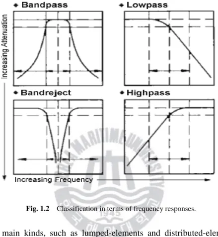
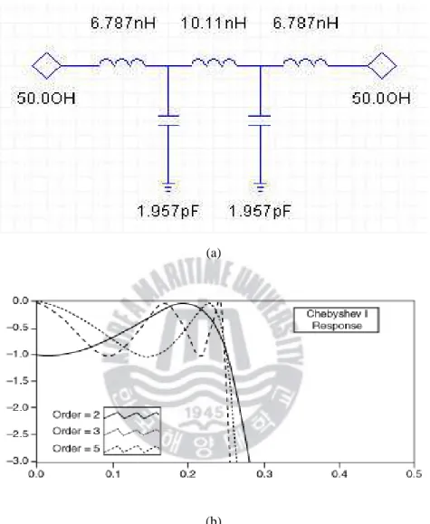
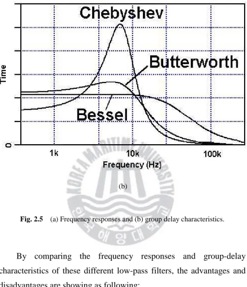
The frequency response of the Butterworth filter is maximally flat (no ripple) in the passband and rolls off to zero in the stopband. However, the Butterworth filter will have a more linear phase response in the passband than Chebyshev Type I/Type II filters and ellipsoids.
Conventional microstrip low-pass filters
2.7 (a) General network topology using lumped elements and (b) a stepped-impedance low-pass filter based on a microstrip line structure. The previous step-impedance low-pass filter realizes the low-pass prototype capacitors as low-impedance lines in the transmission path. Therefore, the next type of low-pass filter based on the structure of microstrip lines is called an open low-pass filter, and its layout is as shown in Fig.
The transformation process and formulas are also all the same with the stepped impedance low pass filters as shown in Fig. The following planar low-pass filter based on microstrip structure is very popular in RF/microwave circuit due to its sharp hull characteristics and high attenuation level. All the three types of the conventional microstrip low pass filters cannot meet the demands of modern microwave circuit.
If we want to realize a low-pass filter with high attenuation and sharp transition band, the combined elements will be six or more. 2.11 (a) Prototype network and (b) circuit layout of low-pass filter with elliptic function based on microstrip line structure.
Compact planar structure
In addition, by combining the open-circuit and symmetrical parallel-coupled circuit equivalent circuit models, a complete equivalent circuit can be achieved in terms of the combined elements L and C, as shown in the figure. In addition, we investigated the frequency responses of the proposed low-pass filter with different apertures. Comparison between two simulated results of the proposed single-unit low-pass filter and its L-C equivalent circuit using.
The physical dimensions of the two-stage low-pass filter can be obtained by the same method used in the one-stage case. 2.24, a comparison is made between the dimensions of the proposed and conventional stepped-impedance low-pass filters. The optimized simulation results of the proposed two-stage low-pass filter are shown in Fig.
Inspecting the simulation results, the two-stage low-pass filter using the proposed structure produces a much sharper skirt characteristic and a deeper suppression band compared with the results of the conventional filter. Therefore, the equivalent circuit needs to be improved to more accurately describe the frequency responses of the proposed compact structure.
Equivalent Circuit Analysis
Equivalent circuit analysis
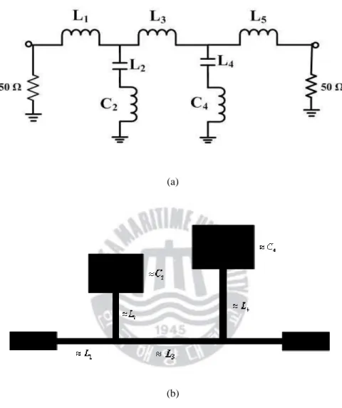
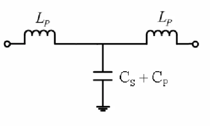
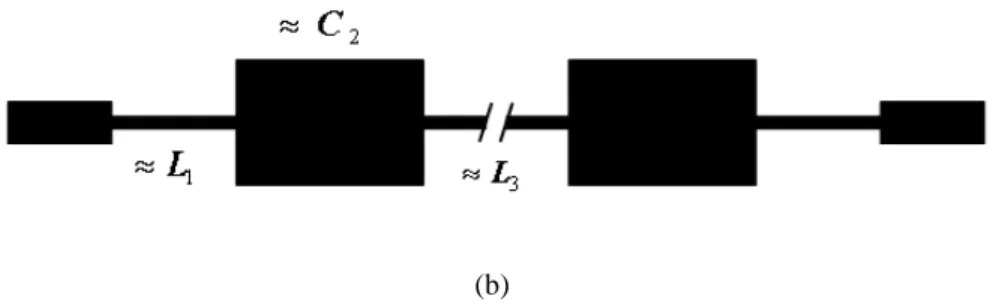
The values of the lumped element model are given in terms of coupled line parameters in a homogeneous medium. Once the clumping elements are determined, any structure that yields the correct clumping element values can be used, whether homogeneous or not. In this case, the parasitic capacitor CC can be eliminated because the far end of the parallel connected line is shorted.
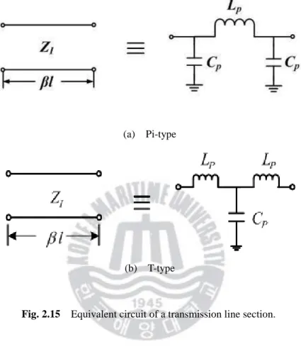
In addition, the other parasitic capacitor Cg can be omitted due to its very small value. Therefore, the parallel coupled line with its end shorted will be approximately modeled as a transformer. Here the current transformer can be transformed into a pi-type network without mutual inductance, as shown in Fig.
The relationship between the transformer and the pi-type network can be obtained from the following equations.
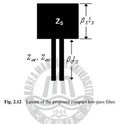
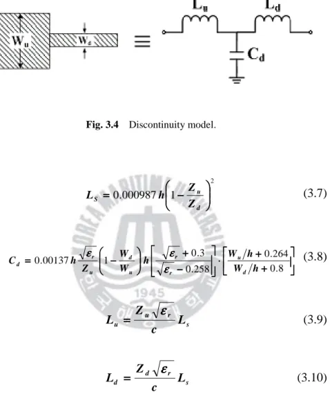
Discontinuity model
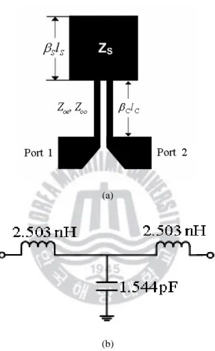
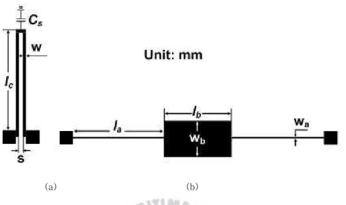
The physical dimensions of the designed compact low-pass filter are shown in Table 1, where the relative dielectric constant is 3.5 and the substrate thickness is 1.524 mm. To examine the validity of the equivalent circuit, a comparison of simulated results was made between the proposed microstrip structure and its equivalent circuit. From figure 3.6, we can find that the simulated results of the proposed low-pass filter depicted as circled line and the simulated results of its equivalent circuit depicted as solid line match very well.
One is by changing the length of the open stub based on the same dimensions of the parallel pair line. To validate the proposed design approach, a microstrip low-pass filter below Cs = 1.20 pF is fabricated based on a 1.524 mm thick Taconic substrate with relative dielectric constant of εr= 3.5. A limited attenuation pole appears at 3.5 GHz up to 53 dB to improve the selectivity characteristic of the low-pass filter.
However, the equivalent circuit composed of lumped elements has its limitations in frequency responses. Because microwave circuits made of distributed elements have a kind of periodic frequency response that cannot be precisely described.
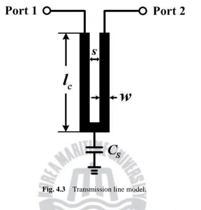
Transmission-Line Model
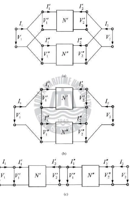
Review of two-port network theory
The ABCD parameters are very useful for analysis of a complex two-port network that can be divided into two or more cascaded subnetworks. Often in the analysis of a filter network, it is convenient to treat one or more filter components or elements as individual subnetworks, and then connect them to determine the network parameters of the filter. This type of connection can be extended to more than two two-port networks connected in parallel.
In that case, the short-circuit admittance matrix of the composite network is simply given by the sum of the short-circuit admittance matrices of the individual networks. Similarly, if there are more than two two-port networks to be connected in series to form a composite network, the open-circuit resistance matrix of the composite network is equal to the sum of the individual matrices of open circuit resistance. For simplicity, consider a network formed by the cascade connection of two sub-networks, as shown in Figure 4.2(c).
It should be noted that the outputs of the first sub-network N' are the inputs of the next second sub-network N'', viz. The transfer matrix of the composite network is therefore equal to the matrix product of the transfer matrices of the cascaded subnetworks.
Transmission line modeling
For the above network, the elements of the impedance matrix [ZU] can be calculated using the even-odd analysis method. From the relationship between the impedance and the scattering matrix, the network transfer parameter can be obtained by [24]. The locations of the carrying zeros are almost identical to those of the intersections shown in Fig.
Therefore, the cutoff frequency can be easily adjusted by choosing a suitable capacitive load, but without changing the sharpness of the cutoff. In order to continuously inspect the effects on the frequency responses of the proposed structure caused by the parallel coupled line, a comparison is made between three different structures with different lengths of the parallel coupled line based on the same capacitive load. 4.8(a), all three crossings shift to the upper frequency as the length of the joined line gradually decreases, especially the second and third.
4.8(c), as the length of the coupled line increases, the cutoff sharpness becomes more abrupt. Through the above graphical analysis, the proposed compact structure can provide a wide repulsion band with three finite attenuation poles, and these finite attenuation poles can be easily adjusted by simply changing the capacitive load value and the length of the coupled line.
Low-pass filter with harmonics suppression
The load capacitor used is a Murata product with its SRF (Series Resonant Frequency) of 6.09 GHz. With its real frequency responses, the semi-lumped compact low-pass filter can be optimized using commercial RF simulator tools. The locations are almost the same as the 2nd, 3rd and 4th harmonics of the cutoff frequency.
Furthermore, any unwanted frequency can be eliminated using this type of circuit by effectively adjusting the parameters of the electrical circuit.
Conclusions
18] Jyh-Wen Sheen, “A Compact Semi-Lumped Low-Pass Filter for Harmonics and Spurious Suppression,” IEEE Microw. 22] Kun-Hui Yi; Bongkoo Kang, “Compact microstrip low-pass filter with sharp rejection characteristics,” IEEE Microw. 10] Rui Li, Dong Il Kim, and Joong Sung Jeon, "Compact Low Pass Filter for Harmonic and Spurious Suppression".
11] Rui Li, Dong Il Kim and Chang-Mook Choi, “Semi-stacked low-pass filter for harmonic suppression”, Journal of the Korea Electromagnetic Engineering Society, October 1] Rui Li, Dong Il Kim and Chang-Mook Choi, “Compact low-pass filter with sharp edge characteristics and wide stopband,” International Journal of Navigation and Port Research, p. Edge Features, “Asia-Pacific.
3] Rui Li and Dong Il Kim and Chang-Mook Choi, “A new compact low-pass filter and its equivalent circuit”, Asian Navigation Conference 2006, Jezu, Korea, p. 7] Rui Li, Dong Il Kim, and Chang-Mook Choi, “Compact Low-Pass Filter for Harmonic Suppression,” Asia-Pacific Microwave Conference 2006, Yokohama, Japan, Dec.
S, ABCD, Y, and Z parameters
Useful two-port networks