Introduction
Related Works
Ternary Device
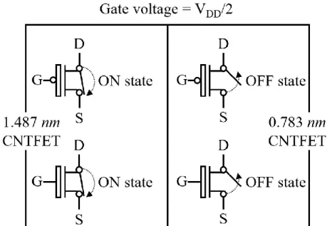
In the structure of CNTFET, semiconducting single-walled carbon nanotubes (SWCNT) are inserted into electronic devices such as a structure of MOSFET [18]. The chirality vector is expressed as a pair of an integer (n, m), which means the angle of the arrangement of carbon atoms in the tube. CNTFETs with a diameter of 0.783 nm, 1.487 nm are used to switch each network of the circuits.
Ternary Gate
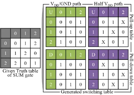
7 shows the structure of a static ternary gate consisting of the VDD/GND path and the half VDD path. The half VDD path pull-up/down networks simultaneously enter the ON state, allowing the output to be half VDD through diode-connected transistors. The switching table shows the switching conditions of the pull-up/down networks to obtain each output value.
When the pull-up network for the VDD/GND path is ON state, the pull-up network for the half VDD path can be ON state or OFF state. The structure of the static ternary gate composed of the VDD/GND path and the half VDD path. Each SOP expression can be calculated as the sum of the operators multiplied by one.
8, the STI is synthesized with six transistors when the 'X' of the switchboard is in the ON state. 9 shows the switch table of pull and pull networks for a ternary SUM gate. PDP (power delay product) is calculated by a product of average power and worst case delay.
We calculated the power delay product (PDP) which is the product of the worst case delay and the average power consumption of the circuits. The frequency of the ternary clock signal used in QETDFF is 25 MHz and the clock signal is 7 ps faster than the input signals to provide a setup time difference.
Methodology of Static Ternary Gate Design
Characteristic Modeling of Ternary Device
The operation of the ternary devices can be modeled as an ON/OFF switching operation where the current flow between the source and the drain is controlled according to the gate voltage. However, when the gate voltage is half of VDD, the 1.487 nm diameter CNTFET becomes ON state and the 0.783 nm diameter CNTFET becomes OFF state. Moreover, in [6], a CNTFET with a diameter of 1.018 nm and a chirality vector of (13, 0) has been proposed for voltage division instead of resistance.
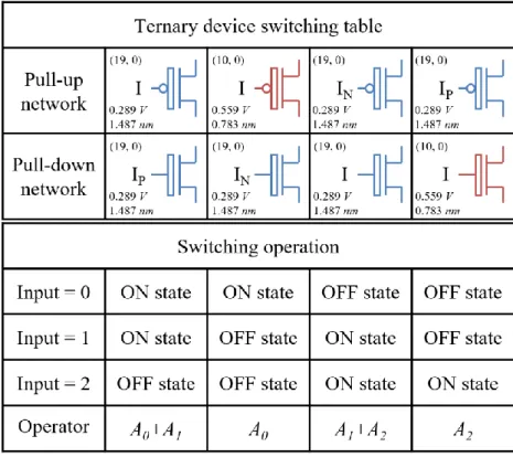
The negative ternary inverter (NTI) and positive ternary inverter (PTI) circuits proposed in [6] are connected to the gate of the CNTFET devices to implement additional switching operations with a small number of transistors. When the gate voltage is half VDD, the two CNTFETs become different ON/OFF states. 6, I is the input value of the gate voltage, IN is the input value of the gate voltage through NTI, and IP is the input value of the gate voltage through PTI.
The switching operator Ai in equations represents the ON/OFF state of a circuit when a specific input value is received. Conditions with more than one ON state for certain input values can be expressed as the sum of the switching operators. When two or more transistors are connected in series, the pull-up/down networks become ON state when all transistors are in ON state.
When two or more transistors are connected in parallel, the pull-up/down networks are in the ON state, even if only one transistor is in the ON state. To implement all switching operations, two or more transistors are connected in series or parallel.
Single Input Ternary Gate Design
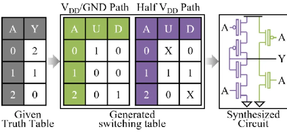
The calculated SOP expression is mapped to the ternary device switching table shown in the figure. On the other hand, it is synthesized with eight transistors when it is in the off state. The sum of the operators represents the parallel connection of the transistors, and the product represents the series connection of the transistors.
Multi-input Ternary Gate Design
To analyze our ternary design methodology, we synthesized several arithmetic logic gates, including a ternary full adder and a ternary multiplier. 14 shows the degree of reduction in the normalized PDP of the proposed designs compared to previous works for each load capacitor, 2 fF and 3 fF. Since the inverted enable signal is GND, TG2 breaks the parallel STI loop and the transferred value can be written.
Therefore, QETDFF can respond to all edges of the ternary clock signal, because the latch responding to 'From Half VDD Edge' and the latch responding to 'To Half VDD Edge' operate alternately. The average power consumption and power consumption were measured from 10 ns to 130 ns to exclude initial values in the simulation of QETDFF. We moved the temporal timing of the input signal to find a margin for the setup time and a margin for the hold time.
The setup time margin of QETDFF is 7 ps and the hold time margin is 11 ps. The worst delay condition is that the triplet clock signal changes from zero to one and the output value changes from zero to one. The waveforms show that the operation of the proposed serial ternary adder is fast and accurate, with few errors generated in the setup time margin.
This is because many capacitors are used in the design of [21] and the circuit is not designed with a static gate. Wong, “A compact SPICE model for carbon nanotube field-effect transistors including non-idealities and its application, Part I: Model of the intrinsic channel region,” IEEE Trans.
Ternary Combinational Circuit
Simulation Setup
Since our methodology is applicable to all new devices that support ternary logic, we have synthesized the circuit using CNTFET and T-CMOS. VDD is 0.9 V and input pattern of [11] and transition time 0.01 ns is used for simulation.
Ternary Full Adder Design & Simulation Result
The standard ternary full adder consists of two half adders and a NANY gate, and a half adder consists of a SUM gate and an NCARRY gate. Our proposed design shows 49% PDP reduction compared to the design of [7] which is based on a transmission gate. It can be seen that the static gates used in the proposed design are more efficient than the gates proposed in the previous works.

Ternary Multiplier Design & Simulation Result
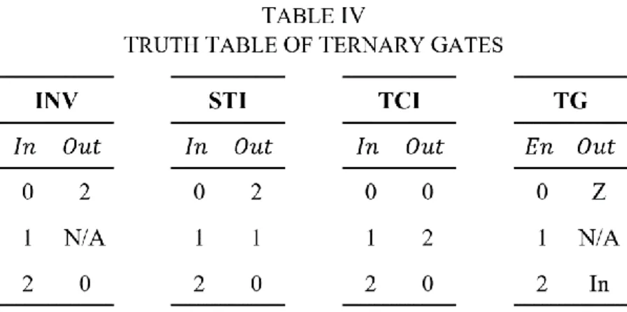
Ternary clock inverter is designed as a static gate to satisfy the truth table of Table IV. Two ternary D-latches whose output value is controlled by a transmission gate are connected in parallel to the input node and the inverted output nodes. The operation of ternary D-latch consists of two phases: the first phase writes a value into the circuit, and the second phase is the transfer of the written value to the output STI.
At this time, TG3 disconnects the path to the reverse output node, and the written value cannot be transferred to the output STI. Because reverse enable signal is VDD, TG2 connects the loop of back-to-back STI. Reverse enable signal is VDD when the ternary clock signal is half VDD, otherwise it is GND.
Thus, the enable signal is GND when the ternary clock signal is half VDD, otherwise it is VDD. In this layout, only metal 1 is visualized and the λ-based scale is used to normalize the size. In particular, the distance between the pull-up network and the pull-down network in this CNTFET layout is only 3λ, which is quite short distance compared to 10λ in normal CMOS layout.
The total energy consumption was calculated, which is the product of the total simulation time and the average energy consumption. As mentioned earlier, when a ternary clock signal can be generated with a sinusoidal signal, the total power consumption of the QETDFF can be reduced to 1/4 compared to a single-edge-triggered ternary flip-flop using a binary clock signal.
Ternary Sequential Circuit
Quad-Edge-Triggered Ternary Sequential Circuit Design
The quad-edge triple D flip-flop design consists of four logic gate inverter (INV), standard triple inverter (STI), transmit gate (TG) and triple clock inverter (TCI). A 1.487 nm diameter CNTFET is used for fast operation of the inverter and transmission gate. The enable signal that controls the operation of the transmit gate consists of VDD and GND.
When the enable signal is half of VDD, the VGS of the transmission port is low and the transmission speed becomes low. In the first phase, the enable signal is VDD, and TG1 sends a value from the input node to back-to-back STI. At this time, the written value sent by TG1 in the first phase is strongly held by the back-to-back STI.
Then TG3 transmits the written value from the back-to-back STI to the inverted output node. Two ternary D-latches whose output value is controlled by a transmission gate always receive different enable signals.
Simulation Setup
Simulation Results of QETDFF
Simulation Results of Ternary Serial Adder
In this thesis, we propose an optimized gate design methodology for the synthesis of ternary logic circuits. Our proposed methodology can be applied to all emerging devices supporting ternary logic (e.g. CNTFET, QDGFET and T-CMOS). Using our ternary gate design technique, it is possible to synthesize ternary logic circuits with different gates.
In addition, gates can be optimally implemented for balanced ternary logic circuits, which have not been widely explored in previous research. We also compared the number of transistors in our ternary circuits with CMOS-based binary logic circuits and observed that ternary logic circuits have an advantage in the region of increasing digit size. QETDFF increases not only the spatial data density but also the temporal data density of the triple system.
4] S.Kamakar, J.A.Chandy and F.C.Jain, “Design of Ternary Logic Combinational Circuits based on Quantum Dot Gate FETs”, IEEE Trans. 5] S.Shin, E.Jang, J.W.Jeong, B.G.Park, and K.R.Kim, “Compact design of low-power standard ternary inverter based on off-state current mechanism using Nano-CMOS technology,” IEEE Trans. Sridharan, "A synthesis methodology for ternary logic circuits in emerging device technologies" IEEE TCAS-1, PP pp.1-14.
19] Sheng Lin, Yong-Bin Kim, and Fabrizio Lombardi, "A New Design of CNTFET-Based Ternary Logic Gate", Proc. 20] Reza Faghih Mirzaee and Niloofar Farahani, “Design of the Ternary Edge-Triggered D Flip-Flap-Flop for Multiple-Valued Sequential Logic,” Journal of Low Power Electronics pp.36-46.
Conclusion


![Fig. 3. The structure of MOSFET-like CNTFET [21].](https://thumb-ap.123doks.com/thumbv2/123dokinfo/10522843.0/16.892.269.640.716.1082/fig-3-structure-mosfet-like-cntfet-21.webp)
![Fig. 4. The gate level schematic of previous (a) Ternary D Latch [22] and (b) Ternary D Flip-Flop [21]](https://thumb-ap.123doks.com/thumbv2/123dokinfo/10522843.0/17.892.211.676.594.1073/level-schematic-previous-ternary-latch-ternary-flip-flop.webp)