DOI: 10.12928/TELKOMNIKA.v14i4.3230 1292
Implementation and Analysis of Reversible logic Based
Arithmetic Logic Unit
Shaveta Thakral*1, Dipali Bansal2, S.K.Chakarvarti3 1,2
Department of Electronics and Communication Engineering, Faculty of Engineering and Technology, Manav Rachna International University, Faridabad, India
3
EX-Manav Rachna International University, Faridabad, India *Corresponding author, email: [email protected]
Abstract
There is a tremendous growth in fabrication from small scale integration (SSI) to giant scale integration (GSI). It however raises a question of sustainability of Moore's law due to almost intolerable levels of power consumption. Researchers have invented a lot of methods to reduce power consumption and recent technologies are switching to reversible logic. Reversible logic has various applications in fields of computer graphics, optical information processing, quantum computing, DNA computing, ultra low power CMOS design and communication. ALU is considered to be the basic building block of a CPU in the computing environment and portability in computing system highly demands reversible logic based ALU. Modern processors usually have a word length of 32 or 64 bits. Divide and conquer approach principle cascades n number of 1 bit ALU to implement n bit ALU. Several researchers have proposed 1-bit ALU design using various reversible logic gates. This paper aims at categorizing various ways of implementation in VHDL using Xilinx ISE design suit 14.2 tool and comparative analysis of existing 1 bit ALU designs in terms of optimization metrics like power consumption, number of gates, number of constant inputs, number of garbage outputs and quantum cost .ALU realized using carry save adder block is found to be most optimum design in terms of gate count and quantum cost.
Keywords:Reversible logic, ALU, GSI, Quantum cost, optimization metrics
Copyright © 2016 Universitas Ahmad Dahlan. All rights reserved.
1. Introduction
In this paper it is proposed to simulate results of various ALU designs and give a comparative analysis of designs in terms of various parameters like power consumption, number of gates, quantum cost, logic operations and garbage outputs. Main target is to find out ALU design with least quantum cost and identify whether divide and conquer approach fits to cascade n number of 1 bit ALU to configure n bit ALU. Background on Reversible logic, various reversible logic gates used in existing ALU designs and brief description about existing ALU designs are further discussed in section 1.1 and 1.2.
1.1. Background on Reversible Logic
In 1961, Landauer [1] stated that “amount of energy dissipated for every bit erasure during an irreversible operation is given by KTln2 joules where K is Boltzmann’s constant, and T is the operating temperature”. In 1973 Bennett [2] proposed the solution to Landauer statement and showed that KTln2 energy dissipation would not occur, if computation is done in a reversible manner since amount of energy dissipated in a system depends directly on numbers of bits erased during computation. Classical gates like two input AND, OR, NAND, NOR, XOR and XNOR are irreversible as input states can’t be uniquely reconstructed from output states. Here two-bit input state is mapped to one-bit output state leads to the erasure of one bit and consequently loss of energy. This energy loss can be avoided by mapping n bit input states to n bit output states so that input states can be uniquely recovered from output states and under such circumstances, a gate is said to be reversible. The optimization metrics of reversible logic circuits are quantum cost, ancillary input, garbage output etc.
numbers of NOT, Controlled-V, Controlled-V+ and CNOT gates.
To achieve reversibility, It is must to map n bit input states to bit n output states and sometimes every gate output is nor used as input to some other gates nor acting as a useful desired output. These undesired or unused outputs that are deliberately obtained to maintain reversibility criterion of a reversible gate (or circuit) are known as Garbage Outputs. Garbage outputs for any reversible logic circuit should be as low as possible.
To achieve reversibility, It is must to map n bit input states to n bit output states. These constant inputs 0 or 1 which are deliberately applied to maintain reversibility criterion of a reversible gate (or circuit) are known as Ancillary Inputs. Ancillary inputs for any reversible logic circuit should be as low as possible. Reversible logic gates used in existing ALU designs are further discussed.
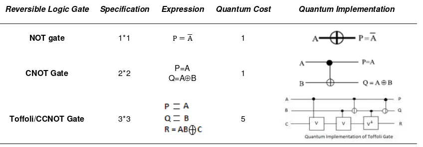
It is very important to know that out of four 1*1 one-qubit gates; only two are reversible i.e. trivial gate and not the gate. Similarly out of 256 possible 2*2 two-qubit gates; only 24 are reversible. There exist 16777216 different 3*3 three-qubit gates however number of reversible 3*3 gates is much smaller i.e.40320. Some popular reversible logic gates that are used in proposed designs of ALU are given in Table 1 with their specification, expression, quantum cost, features and quantum implementation.
Table 1. Popular reversible logic gates used in existing ALU designs
Reversible Logic Gate Specification Expression Quantum Cost Quantum Implementation
NOT gate 1*1 P A 1
CNOT Gate 2*2 P=A
Q=AB 1
Toffoli/CCNOT Gate 3*3 5
1.2. ALU Background and Existing ALU Designs
ALU is a data processing unit, which is an important part in CPU. Different kinds of computers have different ALUs. In logical operations, there are NOT, OR, AND, XOR, etc. while in arithmetic operations there are addition, subtraction, etc. For generating a reversible ALU, each of these general elements, as shown in Figure 1, is buildup with the help of reversible logic. The several sub-modules in the design are adder/Subtractor, Multiplier, and a logical unit.
All the operations are done simultaneously. Depending on the control signal, the needed result is offered at the output.
After a detailed analysis of the various designs of ALU, It has been concluded that each ALU could be divided based on dedicated design and control unit with adder. In the similar fashion these ALUs can also further be divided into two categories, named as: Single line output or Multi line output. So all the possible ALU designs category wise are summarized in Table 2.
Table 2. Categories of Various ALU Designs Design Structure/Number of Output Lines Single Line Output Multi Lines Output
Dedicated Design Paper [16], [17] Paper [19]
Figure 1. ALU block diagram
After an extensive literature survey work is divided into three categories. Brief description about existing ALU designs with these three categories are given in this section. Their simulation and comparative analysis is given in section 2 and conclusion is discussed in section 3.
a) Type 1: Dedicated Design with Single Output
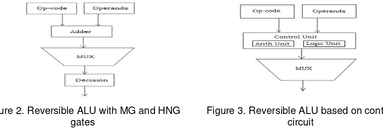
1) Paper [16]: Design of a Novel Reversible ALU using an Enhanced Carry Look-Ahead Adder.
Here authors have proposed a novel 5*5 reversible logic gate popular as MG i.e. Morrison gate that is used in designing of a novel reversible ALU along with HNG gate [16]. This design is verified using Xilinx 14 as shown in Figure 2. Reversible ALU designed with MG and HNG gates performs arithmetic operations such as addition and subtraction and logical operations as AND, OR, NAND, NOR, XOR, and buffer. After that, the comparison heading towards the flowing factors such as the ripple-carry, carry-select, logged stone carry-ahead adders is being observed. Figure 2 shows here with proposed methodology.
Figure 2. Reversible ALU with MG and HNG gates
Figure 3. Reversible ALU based on control circuit
2) Paper [17]: Design1 and Design 2: Reversible Arithmetic Logic Unit
b) Type 2: Control Circuit based Single Output
Paper [18]:An Arithmetic Logic Unit Design Based on Reversible Logic Gates.
Here is this paper, ALU design consists of two main parts i.e. reversible function generator as control unit and reversible mode selection unit. These two parts are cascaded by combinations of Toffoli and NOT gates. Arithmetic and logical operations performed by this ALU
are addition, subtraction, inversion, NOR, NAND, XOR, XNOR, AND, OR, Buffer. Figure 3
shows here with proposed methodology.
Figure 4. Multiplexer based reversible one-bit ALU
Figure 5. Dedicated design with Multi output
c) Type 3: Dedicated Design with Multi Output
Paper [19]:Efficient design of ALU using reversible logic gates.
In this paper ALU is realized with the help of a carry save adder block which are not based on propagation of carry bits. This approach results in improved of 20% and 17% regarding the gate count and quantum cost respectively, while comparing with earlier works in reversible ALU designs. This design has a dedicated unit for the logical and the arithmetic operations, which is a combination of Carry save adder, Fredkin, Toffoli and CNOT reversible logic gates. But having the multiple outputs, to make this ALU functional more gates need to be added so that it can be implemented logically. Figure 5 given above shows here with proposed methodology.
2. Simulation Results and Analysis
All proposed designs are verified using Xilinx 14 with simulation results shown in Figure 6 to Figure 10.
a) Type 1: Dedicated Design with Single Output
1) Paper [16]: Design of a Novel Reversible ALU using an Enhanced Carry Look-Ahead Adder.
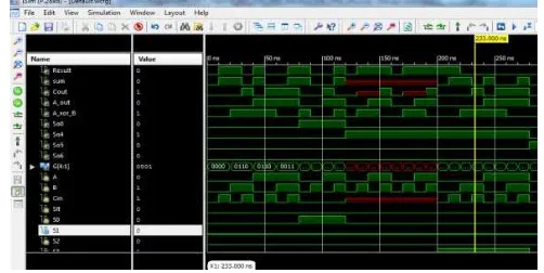
Function table of proposed design as per paper [16] is verified using Xilinx 14 as shown in Figure 6.
2) Paper [17]: Design1 and Design 2: Reversible Arithmetic Logic Unit
Function tables of proposed design 1 and 2 as per paper [17] are verified using Xilinx 14 as shown in Figure 7 and Figure 8 respectively.
Figure 7. Control structure based reversible One-bit ALU
Figure 8. Multiplexer based reversible one-bit ALU
b) Type 2: Control Circuit based Single Output
Paper [18]:An Arithmetic Logic Unit Design Based on Reversible Logic Gates.
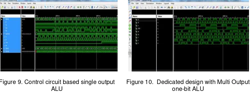
The function table of proposed design as per paper [18] is verified using Xilinx as shown in Figure 9.
Figure 9. Control circuit based single output ALU
Figure 10. Dedicated design with Multi Output one-bit ALU
c) Type 3: Dedicated Design with Multi Output
Paper [19]:Efficient design of ALU using reversible logic gates.
The function table of proposed design of ALU as per paper [19] is verified in Xilinx 14 as shown above in Figure 10.
Logic 0.19 0.02 0.01 0.16 0.06
Signals 0.47 0.07 0.04 0.36 0.18
IOS 34.36 6.95 4.67 57.99 28.49
Total 35.01 7.04 4.72 58.52 28.73
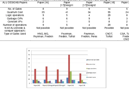
Table 4. Optimization metrics comparison of various ALU designs
ALU DESIGNS/Papers Paper [16] Paper
[17]Design1
Not possible Not possible Not possible Possible Not possible
Type of Gates Used HNG, MG,
Figure 11. Comparative analysis of various ALU designs
3. Conclusion
This paper aims at critical review in terms of categorizing various ways of designing, implementation and comparative analysis of existing 1 bit ALU designs using optimization metrics like power consumption, number of gates, number of constant inputs, number of garbage outputs and quantum cost using Xilinx ISE design suit 14.2 tool. Divide and conquer approach principle cascades n number of 1 bit ALU to implement n bit ALU which is latest in demand of all advanced processors .It is only possible in paper [18] yet quantum cost obtained is very high. ALU realized using carry save adder block in design 3 is found to be most optimum design in terms of gate count, garbage output and quantum cost. Optimization algorithm like ACO and parity preserving for fault tolerance are future prospective would prove to be significant in improving performance of smart ALU for crypto processor.
References
[1] Landauer R. Irreversibility and Heat Generation in the Computing Process. IBM Journal of Research and Development. 1961; 5(3): 183-191.
[2] Bennett C. Logical Reversibility of Computation. IBM Journal of Research and Development. 1973; 17(6): 525-532.
[4] Belayet Ali M. Design of Reversible Sequential Circuit Using Reversible Logic Synthesis.
International Journal of VLSI Design & Communication Systems. 2011; 2(4): 37-45. [5] Peres A. Reversible logic and quantum computers. Phys Rev A. 1985; 32(6): 3266-3276.
[6] Saligram R, TR R. Novel Code Converter Employing Reversible Logic. International Journal of Computer Applications. 2012; 52(18): 24-29.
[7] Biswas K, Hasan M, Chowdhury A, Hasan Babu H. Efficient approaches for designing reversible binary coded decimaladders. Microelectron. 2008; 39(12): 1693-1703.
[8] Susan Christina X, Sangeetha Justine M, Rekha K, Subha U, Sumathi R. Realization of BCD adder using Reversible Logic. International Journal of Computer Theory and Engineering. 2010; 2(3): 1793-8201.
[9] M K. A Novel Reversible Full Adder Circuit for Nanotechnology Based Systems. Journal of Applied Sciences. 2007; 7(24): 3995-4000.
[10] Sharmin F, Mitra R, Hasan R, Rahman A. Low Cost Reversible Signed Comparator. International Journal of VLSI Design & Communication Systems. 2013; 4(5): 19-33.
[11] Dehghan B, Roozbeh A, Zare J. Design of Low Power Comparator Using DG Gate. Scientific Research Circuits and Systems. 2014: 7-12.
[12] Pandey N, Dadhich N, Zubair Talha M. Realization of 2-to-4 reversible decoder and its applications. International Conference on Signal Processing and Integrated Networks (SPIN). 2014: 349-353. [13] Oklobdzija V. Design of High-Performance Microprocessor Circuits. IEEE Press. 2000.
[14] Thomsen M, Glück R, Axelsen H. Reversible arithmetic logic unit for quantum arithmetic. Journal of Physics A: Mathematical and Theoretical. 2010; 43(38): 382002.
[15] Wille R, DrechslerI R. Towards a Design Flow for Reversible Logic. London, New York: Springer. 2010.
[16] Matthew M, Matthew L, Richard M, Nagarajan R. Design of a Novel Reversible ALU using an Enhanced Carry LookAhead Adder. 11th IEEE International Conference on Nanotechnology Portland Marriott. Portland, Oregon, USA. 2011.
[17] Syamala Y, Tilak A. Reversible Arithmetic Logic Unit. 101109/ICECTECH20115941987. Kanyakumari: IEEE. 2011: 207-211.
[18] Guan Z, Li W, Ding W, Hang Y, Ni L. An arithmetic logic unit design based on reversible logic gates. Communications, Computers and Signal Processing (PacRim). 2011 IEEE Pacific Rim Conference on. Victoria, BC. 2011: 925-931.