ZnO 소재는 박막 트랜지스터, 발광소자, 투명전극, 수광소자, 가스센서, 태양전지 등 다양한 응용분야에 응용될 수 있다. 기존 비정질 실리콘 기반 디스플레이의 백플레인 요소를 대체하기 위해 박막 트랜지스터가 활발히 연구되고 있습니다. 그러나 ZnO 박막은 저온에서 성장한 박막임에도 불구하고 기존 비정질 실리콘의 이동도를 뛰어넘고, 공정 비용도 LTPS 공정에 비해 저렴하며, 기존 비정질 실리콘 처리 인프라를 그대로 활용할 수 있기 때문에, 산화물 기반 트랜지스터는 디스플레이에 사용될 수 있으며, 백플레인 장치를 개발하기 위해 많은 연구가 진행되고 있습니다.
또한, ZnO 기반 트랜지스터를 스위칭 소자로 사용하면 MISFET(금속-절연체-반도체 전계 효과 트랜지스터)로 구현될 수 있다. 이러한 박막트랜지스터를 디스플레이 백플레인 소자로 사용하기 위해서는 높은 이동도, 낮은 문턱치 이하 스윙, 높은 ON 전류를 통해 해상도 향상, 낮은 OFF 전류를 통해 전력소모를 감소시키는 소자가 필요하다. MISFET 장치에는 절연층이 필요합니다.
ZnO와 MgxZn1-xO 이종접합박막트랜지스터를 제작하고 ZnO박막의 두께에 따라 소자를 평가하였다. MgxZn1-xO/ZnO TFT 이종접합으로 만들어진 트랜지스터는 게이트 바이어스 스트레스 실험에서 ZnO 디바이스보다 낮은 전류 전달 특성과 낮은 히스테리시스 폭을 나타내는 것으로 확인되었습니다.
Chapter 1. Introduction
Oxide TFT application
Over the past decade, metal oxide semiconductors have attracted much attention for the next generation of backplane flat panel displays. Due to the demands associated with flat panel displays, the need for flexible, transparent displays that can be fabricated using low-temperature, low-cost processes has continuously increased [ 35 , 36 ]. First, oxide materials have high transparency due to a high energy gap > 3.1 eV.
This means that a flexible substrate can be used as a plastic material for the substrate. The screen is developing for large size and high resolution, so high mobility is required.
Comparison of Oxide-based TFT with Si-based TFT
Metal oxide material
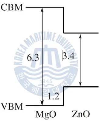
The value of Mg is -2.37 Eo/V, which means that the combination of Mg-O does not lose oxygen easily and Mg can be oxidized more easily than Zn-O. When incorporating Mg into ZnO thin films, the electron traps generated by oxygen vacancy can be reduced, which will improve the stability of the thin film transistor.
Physical properties of ZnO and MgO
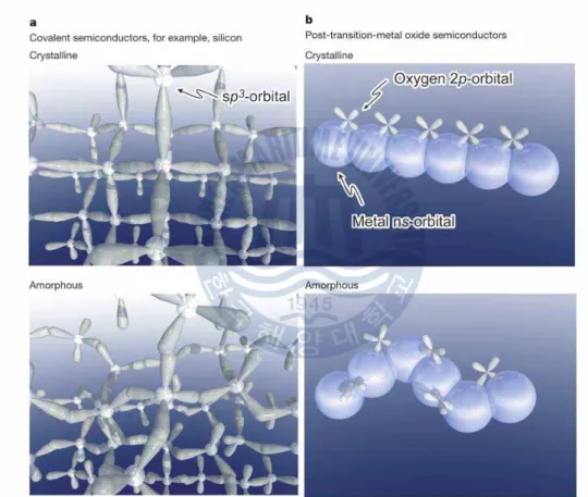
ZnO usually has the hexagonal wurtzite structure in which each Zn or O atom is surrounded by four neighbors of the other type [46]. The band gap width is 3.37 eV and direct, and the minimum of the conduction band is again a single broad minimum formed by Zn s states [7, 47]. The band gap of ZnO can be tuned through divalent substitution at the cation site.
For example, Mg substitution leads to an increase in the band gap up to 4.0 eV while still maintaining the wurtzite structure. This material can be used for gate insulator because of its wide band gap and high dielectric constant. Intrinsic carrier concentration <106 cm-3 Exciton binding energy 60 meV Effective electron mass 0.24 Electron Hall mobility at 300K per.
![Fig. 1.4 Band structure for ZnO [47]](https://thumb-ap.123doks.com/thumbv2/123dokinfo/10547455.0/24.772.184.600.417.762/fig-1-4-band-structure-zno-47.webp)
Application of ZnO
Properties of MgZnO
Heterostructure of MgZnO/ZnO thin films
In this result, the modulation doping structure has shown a high mobility to suppress the impurity potential and the grain boundary potential, regardless of the polycrystallineness of the ZnO layer. Although the MgZnO/ZnO heterostructure is polycrystalline, it shows improved electrical properties for screening defects and grain boundary potential from a large number of carriers caused by the polarization effect [30, 32].
Evaluation of performance for MISFET
Field effect mobility
Saturation Mobility
Threshold voltage
Subthreshold swing
On-off current ratio
- TFT structures and princess
- Experiment method
- Deposition of ZnO and Mg x Zn 1-x O thin films
- Fabrication of TFT devices
- Results and discussion
- Evaluation of MgZnO thin films .1 Structure properties
- Ohmic Contact of MgZnO .1 Motivation
- Single channel layer of MgZnO MISFET .1 Motivation
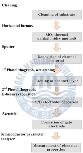
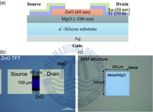
Coplanar structure is that all electrodes are located on the same side of the active. The RF power of the ZnO target was 100 W, which remained unchanged, whereas the power of the MgZnO target was set to 50 or 100 W. Sixth, the gate metal was silver, which was deposited on the back side of the silicon substrate.
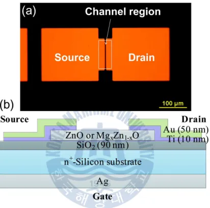
2.3 (a) Top view image of MgZnO-TFT measured by optical microscope (b) Schematic diagram of MgZnO TFT structure. This result means that the crystallinity of the co-sputtered MgZnO thin films is similar compared to the ZnO thin films. The surfaces of ZnO, MZO50 and MZO100 films on SiO2/Si substrates were investigated using AFM measurements.
The surface of the MgxZn1-xO alloy film reveals grain-shaped islands as shown in the figure. In addition, ZnO has potential applications in display devices due to its high transmittance (<80% in the visible wavelength range). Furthermore, we describe the properties of the MgZnO TFT as a function of the Mg content of the ZnO active layer and the structural features of the MgZnO active layer fabricated by the co-sputtering technique.
The RF power of the ZnO target was 100 W, which remained unchanged, while the power applied to the MgZnO target was set to 50 or 100 W. The gate metal was silver, which was deposited on the back side of the silicon substrate. To confirm the density of traps caused by Mg incorporation in the ZnO channel layer, we measured the density of the interfacial and the semiconductor bulk traps (Nt) from the experimental S.S.
The ratio of conduction band offset (DEC) to valence band offset (DEV) between MgZnO and ZnO was previously estimated to be approximately 3:2 [24]. At the MZO50/ZnO interface (i.e. the conduction band location), a localized high electron density can be formed due to the attraction of electrons by the potential arising from spontaneous and/or piezoelectric polarization. However, electron accumulation is also expected at the conduction band edge of the junction interface of ZnO and MZO50 in the two-layer structure.
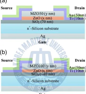
This was due to the low trap density in the drain-source current path localized in the conduction band region of the MZO50/ZnO junction interface. This was due to less efficient carrier confinement at the MZO50/ZnO junction interface due to the attenuation of the electric field at larger distances from the insulator-semiconductor junction interface. The thickness of the ZnO layer had a strong effect on the TFTs, and it was optimized here at ~10 nm.
The SS values of the MZO100/ZnO bilayer TFTs decreased to 0.22 Vdecade-1 compared to the SS of 0.44 V/decade exhibited by the ZnO TFT.
![Fig. 1.8 TFT structures (a) staggered bottom-gate (invert), (b) coplanar bottom-gate (invert), (c) staggered top-gate, and (d) coplanar top-gate [52]](https://thumb-ap.123doks.com/thumbv2/123dokinfo/10547455.0/36.772.148.643.351.642/fig-structures-staggered-invert-coplanar-invert-staggered-coplanar.webp)
Chapter 3. MgO Insulator
Study of TFTs by using a MgO insulator
- Motivation
- Experimental detail
- Results and Discussion
- Conclusion
This result showed superior transparency in the visible range regardless of the different oxygen to argon percentage deposition conditions. The MgO thin film grown with 70% oxygen showed the lowest RMS value. These results indicated that the interaction between Mg2+ and O2- was more active in the oxygen-enriched environment, which explains the increase in MgO thickness.
To investigate the gate insulating dielectric properties, capacitance-frequency (C-f) measurements were performed using the MIM structure. 3.1) where C is the capacitance, e0 is the dielectric constant in vacuum, er is the dielectric constant, A is the contact area and d is the distance. The dielectric constant increased as the percentage of oxygen in the reactive gas mixture was increased. The output characteristics revealed that the ZnO-TFTs exhibit saturation characteristics, as illustrated by the flatness of the IDS.
In the saturation region at VGS = 10 V, the IDS for the ZnO TFT made with an oxygen percentage of 70% were three times higher than the values for the other ZnO TFTs (oxygen percentages of 30% and 50%). However, none of the TFT devices showed an increase in IDS after comparison. 2), due to the presence of electron traps. This phenomenon could be due to the electron injection from the ZnO channel layer into the gate oxide that occurred when the VGS increased [82].
μFE values for ZnO TFTs with MgO insulator grown using 30% oxygen percentage. The mobility improvement is likely due to two factors: the increase in dielectric constant, which would have increased the accumulation of electrons in the ZnO channel layer, and the decrease in trap density, which occurred due to compensation effects; i.e., the effects of oxygen vacancy defects in the channel layer were compensated by the injection of excess oxygen ions into the MgO insulator at the ZnO/MgO interface. The ION/IOFF ratios of ZnO TFTs with MgO insulators grown using 30% and 50% oxygen percentages were similar (approximately 104), while the ZnO TFT device with 70% oxygen percentage showed a value of ~105, due to of higher current generated compared to other devices.
In summary, ZnO TFTs with MgO insulators were successfully fabricated with different oxygen percentages in the reactive gas mixture, using RF magnetron sputtering. The MgO insulator properties were controlled by changing the oxygen percentage in the reactive gas mixture. The Mg composition of the ZnO thin films was monitored using ZnO and Mg0.3Zn0.7O targets sputtered together under variable applied RF power.
![Table 1.1 Comparison of oxide-based TFT with Si-based TFT for number of process step, cost, mobility, and etc [37]](https://thumb-ap.123doks.com/thumbv2/123dokinfo/10547455.0/19.772.111.670.442.817/table-comparison-oxide-based-based-number-process-mobility.webp)
![Fig. 1.3 The crystal structure (a) cubic rock salt, (b) cubic zinc blende, and (c) hexagonal wurtzite structure [46]](https://thumb-ap.123doks.com/thumbv2/123dokinfo/10547455.0/23.772.113.643.438.791/crystal-structure-cubic-cubic-blende-hexagonal-wurtzite-structure.webp)
![Fig. 1.7 (a) 2DEG concentration and (b) Hall mobility of ZnO/MgZnO single heterostructure [26]](https://thumb-ap.123doks.com/thumbv2/123dokinfo/10547455.0/31.772.204.592.167.740/fig-2deg-concentration-hall-mobility-mgzno-single-heterostructure.webp)